DA9122.003
6 November 2002
1 (12)
MAS9122
3-Output LDO Voltage Regulator IC
∑
Three Low Dropout Voltage
Regulators
∑
Very Low Noise: 25 µVrms
∑
High Ripple Rejection: 63 dB
∑
Very Low Crosstalk
∑
Low Ground Pin Current
∑
Regulator Enable/Disable
Control
DESCRIPTION
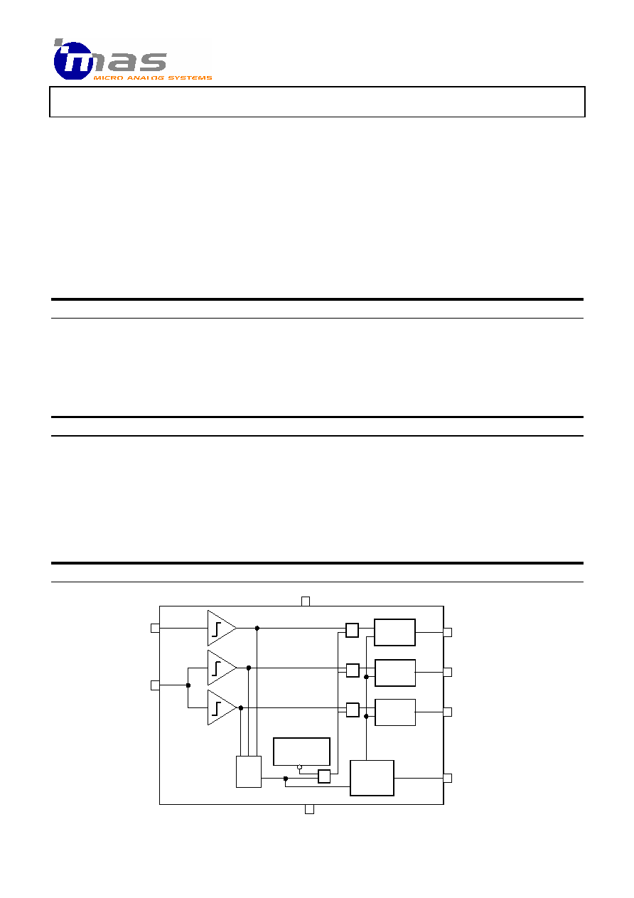
MAS9122 is a three-output voltage regulator. It is
designed for three different output voltages, which
can be modified through a mask option. Regulators
operating mode is controlled by two enable/disable
pins. The circuit consists of a bandgap voltage
reference, an error amplifier, a current limit circuit
and a thermal protection circuit.
MAS9122 features very low ground pin current:
typically less than 1.5 µA sleep mode current and
typical 125 µA for one regulator in active mode.
Excellent noise and PSRR performance enables the
use of MAS9122 in high precision portable devices.
Low crosstalk between regulators provides an area
efficient solution compared to single regulators.
FEATURES
APPLICATIONS
∑
Three Regulators at 135 mA, 70 mA and 50 mA
∑
Output Options 2.70, 2.85 and 3.00 V, see
Ordering Information p. 12
∑
Low Noise: 20 µVrms Typical and
30 µVrms Maximum for All Regulators over
Frequency Range 100 Hz...100 kHz
∑
Fast Dynamic Response
∑
Output Voltage Accuracy <
±
2.0 %
∑
MSOP-8
Package
∑
Systems Requiring Stabilized Power in
Separate Blocks
∑
Cordless
Phones
∑
Mobile
Phones
∑
Portable
Systems
∑
Battery Powered Systems
BLOCK DIAGRAM
LDO_A
LDO_B
LDO_C
135 mA
70 mA
50 mA
OUT A
OUT B
OUT C
VREF
&
&
&
Bandgap
Reference
Temperature
Protection
&
OR-
gate
ENA
ENBC
VIN
GND

DA9122.003
6 November 2002
2 (12)
PIN CONFIGURATION
Top Marking Information:
AX = voltage version, see p.12 Ordering information
WW = week
PIN DESCRIPTION
Pin Name
Pin
Type
Function
OUTA
1
O
135 mA Regulator Output
OUTC
2
O
50 mA Regulator Output
ENBC
3
I
Enable for Regulators B and C
ENA
4
I
Enable for Regulator A
VREF
5
O
Reference Voltage: Pin for Bypass Capacitor
GND
6
P
Ground
VIN
7
P
Positive Supply Voltage
OUTB
8
O
70 mA Regulator Output
ABSOLUTE MAXIMUM RATINGS
All Voltages with Respect to Ground
Parameter
Symbol
Conditions
Min
Max
Unit
Supply Voltage
V
IN
-
0.3
6
V
Voltage Range for All Pins
-
0.3
V
IN
+ 0.3
V
ESD Rating
HBM
2
kV
Junction Temperature
T
Jmax
175
(limited)
o
C
Storage Temperature
T
S
-
55
+150
o
C
Stresses beyond those listed may cause permanent damage to the device. The device may not operate under these conditions, but will not
be destroyed.
RECOMMENDED OPERATING CONDITIONS
Parameter
Symbol
Conditions
Min
Max
Unit
Supply Voltage
V
IN
V
OUT(NOM)
+ 0.25
5.3
V
Operating Junction
Temperature
T
J
-
40
+125
∞C
Operating Ambient
Temperature
T
A
-
40
+85
∞C
OUTA 1
OUTC 2
ENBC 3
ENA 4
8 OUTB
7 VIN
6 GND
5 VRF
9
1
2
2
A
X
W
W
Top View
G = Ground, I = Input, O = Output, P = Power
DA9122.003
6 November 2002
3 (12)
ELECTRICAL CHARACTERISTICS
x
Thermal Protection
T
A
= -40∞C to +85∞C, typical values at T
A
= +27∞C, V
IN
= 4.5 V, I
OUT
= 1.0 mA, C
IN
= 1.0 µF, C
L
= 1.0 µF, C
BYPASS
= 10 nF,
V
CTRL
= 2.0 V, unless otherwise specified.
Parameter
Symbol
Conditions
Min
Typ
Max
Unit
Threshold High
T
H
130
150
170
o
C
Threshold Low
T
L
120
140
160
o
C
The hysteresis of 10
o
C prevents the device from turning on too soon after thermal shut-down.
x
x
x
x
Control Pin Parameters
T
A
= -40∞C to +85∞C, typical values at T
A
= +27∞C, V
IN
= 4.5 V, I
OUT
= 1.0 mA, C
IN
= 1.0 µF, C
L
= 1.0 µF, C
BYPASS
= 10 nF,
V
CTRL
= 2.0 V, unless otherwise specified.
Parameter
Symbol
Conditions
Min
Typ
Max
Unit
Input Voltage
ON-state
OFF-state
ENA,
ENBC
-
0.3
2.0
V
IN
+ 0.3
0.3
V
If CTRL-pin is not connected, the particular regulator(s) is/are in OFF state (900 k pull-down resistor to ground).
x
Current Parameters
T
A
= -40∞C to +85∞C, typical values at T
A
= +27∞C, V
IN
= 4.5 V, I
OUT
= 1.0 mA, C
IN
= 1.0 µF, C
L
= 1.0 µF, C
BYPASS
= 10 nF,
V
CTRL
= 2.0 V, unless otherwise specified.
Parameter
Symbol
Conditions
Min
Typ
Max
Unit
LDO_A Continuous Output Current
I
OUTA
0
135
mA
LDO_B Continuous Output Current
I
OUTB
0
70
mA
LDO_C Continuous Output Current
I
OUTC
0
50
mA
Short Circuit Current for LDO_A
I
SHORTA
350
mA
Short Circuit Current for LDO_B
I
SHORTB
265
mA
Short Circuit Current for LDO_C
I
SHORTC
230
mA
Ground Pin Current
I
GND(OFF)
I
OUT
= 0 A, V
ENA,ENBC
< 0.3 V,
V
IN
= 3.6
2
4
µA
Ground Pin Current
I
GND(ONA)
I
OUT
= 0 A, V
ENA
> 2 V,
V
ENBC
< 0.3 V, V
IN
= 3.6
125
µA
Ground Pin Current
I
GND(ONBC)
I
OUT
= 0 A, V
ENA
< 0.3 V,
V
ENBC
> 2 V, V
IN
= 3.6
170
µA
Ground Pin Current
I
GND(ONABC)
I
OUT
= 0 A, V
ENA, ENBC
> 2 V
V
IN
= 3.6
245
µA

DA9122.003
6 November 2002
4 (12)
x
x
x
x
Voltage Parameters
T
A
= -40∞C to +85∞C, typical values at T
A
= +27∞C, V
IN
= 4.5 V, I
OUT
= 1.0 mA, C
IN
= 1.0 µF, C
L
= 1.0 µF, C
BYPASS
= 10 nF, V
CTRL
= 2.0 V,
unless otherwise specified.
Parameter
Symbol
Conditions
Min
Typ
Max
Unit
Output Voltage:
Mask option for 2.85 V
V
OUTA
V
OUTA,B,C
Max I
OUT
= 135 mA
Max I
OUTA
= 100 mA, Max I
OUTB
=
70 mA, Max I
OUTC
= 50 mA
2.85 ≠ 3%
2.85 ≠ 2%
2.85
2.85
2.85 + 2%
2.85 + 2%
V
V
LDO_A Dropout
Voltage
V
DROPA
I
OUTA
= 135 mA
I
OUTA
= 100 mA
220
180
mV
LDO_B Dropout
Voltage
V
DROPB
I
OUTB
= 70 mA
165
mV
LDO_C Dropout Volt.
V
DROPC
I
OUTC
= 50 mA
150
mV
x
x
x
x
External Capacitors
T
A
= -40∞C to +85∞C, typical values at T
A
= +27∞C, V
IN
= 4.5 V, I
OUT
= 1.0 mA, C
IN
= 1.0 µF, C
L
= 1.0 µF, C
BYPASS
= 10 nF,
V
CTRL
= 2.0 V, unless otherwise specified.
Parameter
Symbol
Conditions
Min
Typ
Max
Unit
Output Capacitors for
all Regulators
C
OUTA,B,C
0.8
1
µF
Effective Series Resistance
ESR
0.01
0.1
2
Bypass Capacitor
C
BYPASS
10
nF
x
x
x
x
Power Dissipation
T
A
= -40∞C to +85∞C, typical values at T
A
= +27∞C, V
IN
= 4.5 V, I
OUT
= 1.0 mA, C
IN
= 1.0 µF, C
L
= 1.0 µF, C
BYPASS
= 10 nF,
V
CTRL
= 2.0 V, unless otherwise specified.
Parameter
Symbol
Conditions
Min
Typ
Max
Unit
Junction to Case Thermal
Resistance
R
JC
39
∞C/W
Junction to Ambient Thermal
Resistance
R
JA
typical PC board mounting,
still air
206
∞C/W
Maximum Power Dissipation
P
d
any ambient temperature
JA
A
(MAX)
J
MAX
d
R
T
T
P
-
=
mW
Note 1
Note 1: T
J(MAX)
denotes maximum operating junction temperature (+125∞C), T
A
ambient temperature, and R
JA
junction-to-ambient thermal
resistance (+206∞C/W).
x
x
x
x
Load Regulation
T
A
= -40∞C to +85∞C, typical values at T
A
= +27∞C, V
IN
= 4.5 V, I
OUT
= 1.0 mA, C
IN
= 1.0 µF, C
L
= 1.0 µF, C
BYPASS
= 10 nF,
V
CTRL
= 2.0 V, unless otherwise specified.
Parameter
Symbol
Conditions
Min
Typ
Max
Unit
Load Regulation LDO_A
0 mA < I
OUT
< 135 mA
0 mA < I
OUT
< 100 mA
22
22
50
30
mV
Load Regulation LDO_B
0 mA < I
OUT
< 70 mA
21
25
mV
Load Regulation LDO_C
0 mA < I
OUT
< 50 mA
13
22
mV
x
x
x
x
Line Regulation
T
A
= -40∞C to +85∞C, typical values at T
A
= +27∞C, V
IN
= 4.5 V, I
OUT
= 1.0 mA, C
IN
= 1.0 µF, C
L
= 1.0 µF, C
BYPASS
= 10 nF,
V
CTRL
= 2.0 V, unless otherwise specified.
Parameter
Symbol
Conditions
Min
Typ
Max
Unit
Line Regulation for all LDOs
I
OUT
= I
MAX
,V
IN
from
V
OUT(NOM)
+ 0.35 V to 5.3 V
0.40
1.2
mV

DA9122.003
6 November 2002
5 (12)
x
x
x
x
PSRR
T
A
= -40∞C to +85∞C, typical values at T
A
= +27∞C, V
IN
= 4.5 V, I
OUT
= 1.0 mA, C
IN
= 1.0 µF, C
L
= 1.0 µF, C
BYPASS
= 10 nF,
V
CTRL
= 2.0 V, unless otherwise specified.
Parameter
Symbol
Conditions
Min
Typ
Max
Unit
PSRR for all LDOs
I
OUT
= Max I
OUT
V
IN
= 3.6 V
f = 1 kHz
f = 10 kHz
47
75
63
dB
x
x
x
x
Noise and Crosstalk
T
A
= -40∞C to +85∞C, typical values at T
A
= +27∞C, V
IN
= 4.5 V, I
OUT
= 1.0 mA, C
IN
= 1.0 µF, C
L
= 1.0 µF, C
BYPASS
= 10 nF,
V
CTRL
= 2.0 V, unless otherwise specified.
Parameter
Symbol
Conditions
Min
Typ
Max
Unit
Noise Voltage for all LDOs
V
NO
100 Hz < f < 100 kHz
25
30
µVrms
x
x
x
x
Dynamic Parameters
T
A
= -40∞C to +85∞C, typical values at T
A
= +27∞C, V
IN
= 4.5 V, I
OUT
= 1.0 mA, C
IN
= 1.0 µF, C
L
= 1.0 µF, C
BYPASS
= 10 nF,
V
CTRL
= 2.0 V, unless otherwise specified.
Parameter
Symbol
Conditions
Min
Typ
Max
Unit
Start-up Delay (from enabling
LDO_A to 90% * V
OUT(NOM)
,
other LDOs at ON state)
(Note 2)
V
ENA
from < 0.3 V to > 2.0 V,
V
ENBC
>
2.0 V, I
OUT
= Max I
OUT
,
C
OUTA
= 1 µF
25
µs
Overshoot
V
ENA
from < 0.3 V to > 2.0 V,
V
ENBC
>
2.0 V, I
OUT
= Max I
OUT
,
C
OUTA
= 1 µF
1
%
Settling Time
(from 90% * V
OUT(NOM)A
to max
±0.1% fluctuation)
V
ENA
from < 0.3 V to > 2.0 V,
V
ENBC
>
2.0 V, I
OUT
= Max I
OUT
,
C
OUTA
= 1 µF, w/o C
BYPASS
200
µs
Note 2: When all regulators are disabled the start-up delay is a function of a bypass capacitor. Typically 0.5 ms for 10 nF capacitor.
CTRL
VOUT
50%
start-up delay
90%
overshoot
settling time
Figure 1.
Definitions of
start-up delay, overshoot
and settling time.