 | –≠–Ľ–Ķ–ļ—ā—Ä–ĺ–Ĺ–Ĺ—č–Ļ –ļ–ĺ–ľ–Ņ–ĺ–Ĺ–Ķ–Ĺ—ā: MAS9128 | –°–ļ–į—á–į—ā—Ć:  PDF PDF  ZIP ZIP |
1
DA9128A.002
July 12, 1998
Ę°§£¶•®ß®©®®°
!#"%$'&)(&%$0
"1!2354
6
∑
798A@
BCB%D
E9FHG9@
EAI9EAP9QARCEAD
Q
SCTAB%@
BCTAP9D
SCQ
E9@
U
∑
V1WCXAY9`
aCb
c9deWCfAaCgA`
W2h
iAp
q2aCgA`
W%r2c9fAb
d
cA`
∑
sut9vxw2yu2CC
92
w2wCtA9w
∑
A92
C2A
9d
Ce2d
f
9g
hAiCjlknmAo
prqCo
set
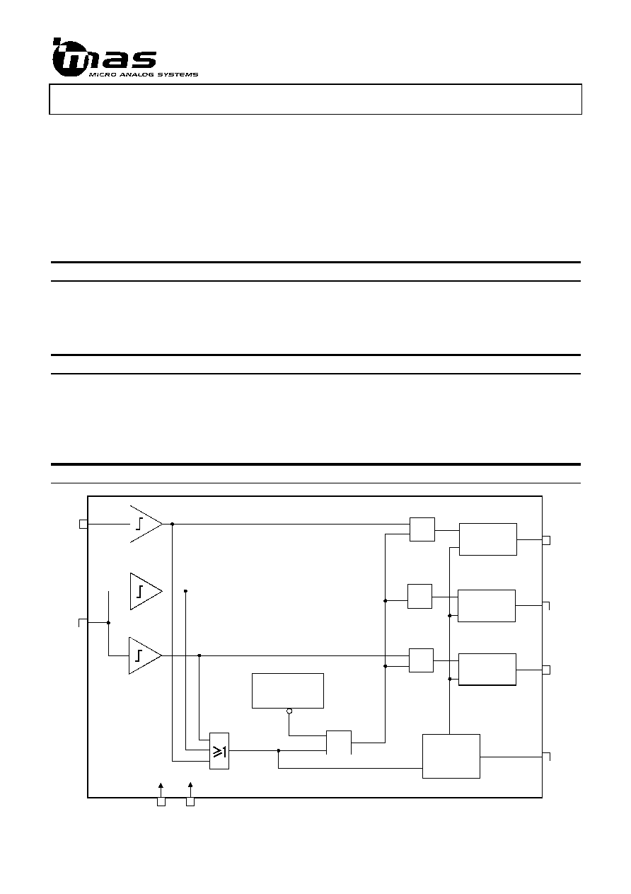
The MAS9128A is voltage regulator IC with three
2.85V LDO regulators providing voltage regulation
for the handset terminal. The output voltages of the
three regulators can be modified through a mask
option. Two enable/disable pins control the state of
the regulators. In order to save power the device
goes into sleep mode when all regulators are
disabled. An internal thermal protection circuit
prevents the device from overheating. The
maximum output current is limited internally.
urvxwAyCzA{AvC|
wu}2}2~x
lwAyC
e
∑
2.85V regulators at 100mA, 70mA and 50mA
∑
Output accuracy <
Ī
3%
∑
Fast dynamic response
∑
Low output noise
∑
Low supply current: 150ĶA per regulator
∑
SO8 package
∑
Mobile phones
∑
Cordless phones
∑
Battery powered systems
Axun5A
Ae2'
&
Bandgap
Reference
LDO_B
(70mA)
OUTB
VREF
ENA
GND
VCC
ENBC
LDO_A
(100mA)
OUTA
LDO_C
(50mA)
OUTC
&
&
Temperature
Protection
&
2
DA9128A.002
July 12, 1998
2
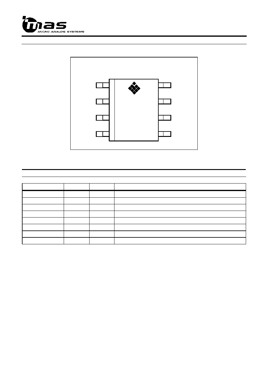
%AeAx
eA2AC
e
1
2
3
4
5
6
7
8
SO8
OUTA
OUTB
OUTC
ENA
ENBC
GND
VCC
VREF
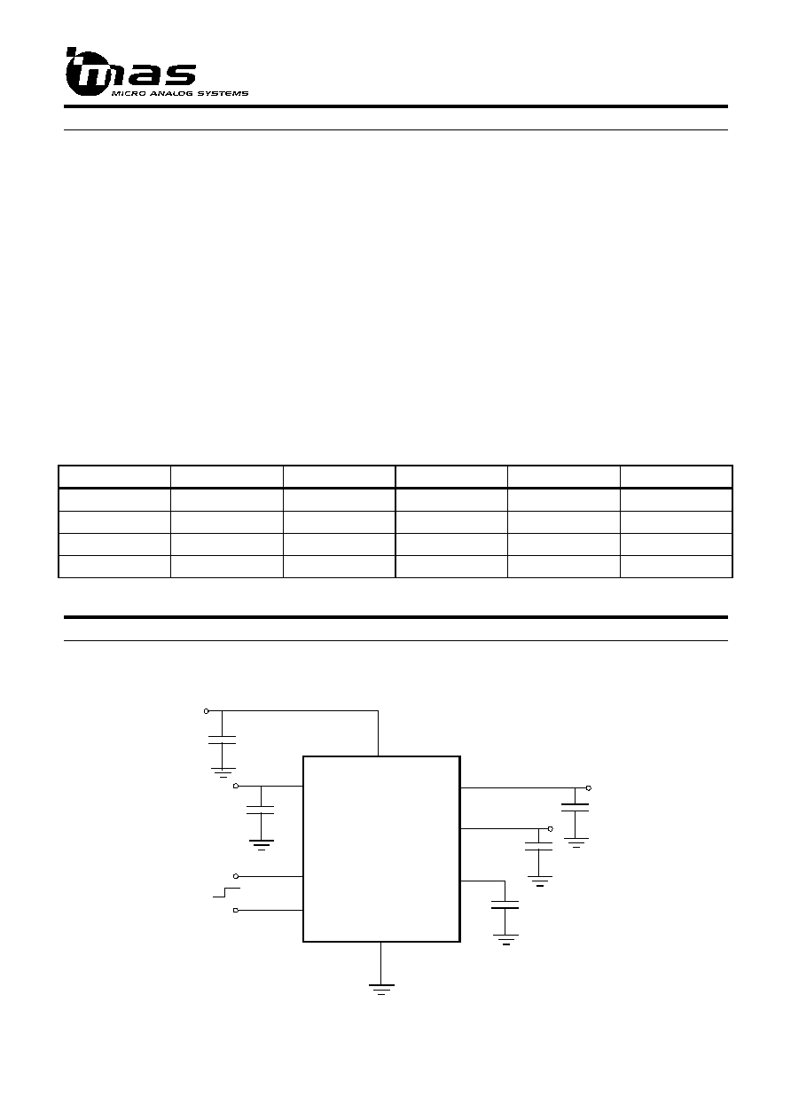
C
5ACln A
r°C
Ęe
£•§
¶nß©®ę™A¨
£©§
¶
#ģįĮ
¨≤Īį≥#¶#ī
Ķ
§
∂©¶
OUTA
1
O
2.85V/100mA regulator output
OUTC
2
O
2.85V/50mA regulator output
ENBC
3
I
Enable for regulators B and C
ENA
4
I
Enable for regulator A
VREF
5
O
Reference voltage
GND
6
P
Ground
VCC
7
P
Positive supply voltage
OUTA
8
O
2.85V/70mA regulator output
3
DA9128A.002
July 12, 1998
∑'łlĻlļeĽrľlĹCĺņŅ'∑9ŃA¬
Ņ1ľAŅń√2∑AĹC¬
Ň9∆'Ļ
(All voltages with respect to ground.)
«#»#…
»ę Aň
Ő
ň#…
Õ•őę 'Ōę–•—
“”–©‘ę’•÷
Ő
÷
–•‘
◊
ōn÷
‘
ōl»
ŔŘŕx‘#÷
Ő
Supply Voltage
V
CC
-0.3
13.0
V
Logic input voltage
V
EN
-0.3
V
CC
+0.3
Max. Junction Temperature
T
J
150
0
C
Thermal resistance
R
JA
163
0
C/W
Lead temperature
for 10 seconds
230
0
C
Storage Temperature
T
S
-55
+150
0
C
ESD Rating
Note 1: Stresses beyond those listed may cause permanent damage to the device. The device may not operate
under these conditions, but will not be destroyed.
‹A›2řAŖeŗŠŗ1›2‚A„A›l„%ŖŠšC›l‹2Ś9ś2Á
Ŗe‚%řAŖe‚A„AÁ
śCÁ
Ŗe‚lŤ
ťįÍ#Ž
ÍęžAŪ
Ó
Ū#Ž
Ô•ūęž'ŮęÚ•ů
۔کűęŲ•ų
Ó
ų
Ú•ű
Ý
ýnų
űŻķ#ūįŁżý9Í
Ģ
ˇxűįų
Ó
Supply Voltage
V
CC
3.1
6.5
V
Operating Temperature
T
AMB
-20
+70
0
C
°£Ę§°¶•®ß©
•£Ę•¶©¶•®ß¶°¶©
£ß
•®
x
! #"%$
&'%(
)%$
0%1
"#2
1
3
0!4
5
'%$
'#&"
1
"%$
687#&9#08(
@A0!4#B83
1
3
084
C
D3
4E%7%)FD®'
GIH§4%3
1
Threshold high
T
H
130
150
170
0
C
Threshold low
T
L
120
140
160
0
C
Continuos power dissipation
in operation
T
AMB
= 25
0
C
644
mW
T
AMB
= 70
0
C
368
mW
NOTE 2:A hysteresis of 10
0
C avoids oscillation in case of thermal shutdown. After the regulator temperature has
dropped by this value, it will turn on again automatically.
x
P§Q
R8Q
S
T%U
V
WYX%`
S
ab
c!d8e§f#c!d§gAh§i
(T
AMB
= -20
0
C to +70
0
C, unless otherwise noted. Typical value for T
J
is 27
0
C.)
pYq%r
q#st
u
t%r
v8w#sx#y8
Ay!#8
u
y8
E%w%F®q
I§%
u
Input high voltage
V
IH
2.2
V
Input low voltage
V
IL
0.40
V
4
DA9128A.002
July 12, 1998
£§¶®
£¶¶®¶¶
£
®
x
d!e
f!g%h
i
j
k8l8m¶g
j
n%g
j
op
qYrAmAs#tvu#q%rAm§s8wAu#q%rAm§sYx§y
(T
AMB
= -20
0
C to +70
0
C, unless otherwise noted. Typical value for T
J
is 27
0
C Cin=1ĶF Cout= 1ĶF,ceramic)
zY{%|
{#}~
~%|
8#}#8
A8%Y
!
%%®{
§%
Output voltage
V
OUT
3.1V < V
CC
< 6.5V,
0mA < I
OUT
< I
MAX
2.7
2.85
3.0
V
Short circuit current
LDO_A
I
MAXA
310
mA
LDO_B
I
MAXB
220
mA
LDO_C
I
MAXC
170
mA
Load Current
LDO_A
I
OUTA
0
100
mA
LDO_B
I
OUTB
0
70
mA
LDO_C
I
OUTC
0
50
mA
Line regulation
1Vpp at V
CC
, max. load
1.1
10
mV
Load regulation
0mA < I
OUT
< I
MAX
LDO_A
9
45
mV
LDO_B
6
31
mV
LDO_C
5
22
mV
Load transient
T
AMB
= 25
o
C
10uA to Ĺ load in 1us
(
4)
-60
mV
100uA to max. Load in 1us (4)
-70
mV
10uA to max. Load in 1us (5)
-85
mV
PSRR
f
10kHz, 1Vpp at V
CC
= 4.5V
CREF = 10nF
50
60
dB
Quiescent current
per regulator
(3)
I
QR
ON, max. load
170
uA
I
QR
ON, I
OUT
= 100uA
150
uA
I
QR
OFF
<1
uA
Total quiescent
current
I
Q
ENA = ENBC = 0V
I
OUT
= 0 V
CC
= 6.5V
<1
30
ĶA
Noise
10Hz < f < 100kHz
typical load, no capacitor at VREF
190
uVrms
10Hz < f < 100kHz
typical load, 10nF cap. at VREF
50
uVrms
Settling time
Enables OFF to ON
2.7V < V
OUT
< 3.0V
10nF cap. at VREF
0.5
1.0
ms
Output capacitor
C
OUT
0.8
1.0
2.6
uF
ESR
0.01
0.1
1
Ohm
NOTE 3:To get the real quiescent current of the device, the quiescent current of the reference voltage generator
(140uA typ.) has to be added together once for all regulators.
NOTE 4:V
OUT
does not drop below 2.7V for more than 1us.
NOTE 5:V
OUT
does not drop below 2.5V for more than 1us or below 2.7V for more than 50us.
5
DA9128A.002
July 12, 1998
v®®
£
-
x
§%Y%
£ !°!
Ę
£
§Y•#¶
!°!
Ę
£
§Y•ß!•
§!%
£
Ę
°8®
©
The device is supplied with 3.1V to 6.5V battery
voltage under normal conditions. An internal band
gap voltage reference is used to generate the
reference voltage for all three voltage regulators.
The reference voltage is routed via an internal
20kOhm Resistor to an external pin where a filter
capacitor can be connected in order to reduce the
noise level of all three regulators. The startup time
of the reference voltage is then determined by the
value of the bypass capacitor at pin VREF.
x
™8ę#¨%%ģ
Įį!Ī
ę
≤
Each regulator can be enabled/disabled by the two
enable pins ENA and ENBC. Pin ENA controls
regulator LDO_A and pin ENBC controls both
regulators LDO_B and LDO_C. If both enable pins
are forced low, the internal voltage reference and
internal bias source are turned off in order to save
power. A common enable for all three regulator
outputs is designed, but connected to VDD
internally for the SOIC8 version of MAS9128A.
x
≥!ī
Ķ8∂Y∑
ł
Ļ
ļ!Ľ
ľ
The device contains three 2.85V low dropout CMOS
regulators with maximum output currents of 100mA,
70mA and 50mA. There is a mask option to modify
the output voltage to 2.55V, 2.70V, 2.85V, 3.00V or
3.15V. The IC has thermal protection in order to
prevent thermal destruction especially at high
ambient temperatures. Maximum output current of
each regulator is limited by an internal circuitry. The
regulation loop of the regulators is optimized to work
with low ESR ceramic buffer capacitors at the
output.
ĹAĺvŅņ
Ѭ
√vńAŇ
∆»«
ĺv…£ £ň!√vńAŇ
∆Őņ
ňvÕAő!¬
Ō
–8—8“
–8—§”A‘
’%÷A◊§ō#“
’%÷A◊§ō8”
’%÷A◊§ōY‘
Ŕ§ŕ§–!Ř
1
1
ON
ON
ON
ON
1
0
ON
OFF
OFF
ON
0
1
OFF
ON
ON
ON
0
0
OFF
OFF
OFF
OFF
‹ř›¶›¶Ŗ§ŗ
Š£‹‚ŗ
„šŚŗ
šś§„ÁŤ‹‚ŗ
„š
ť¶ÍvŽ8ž%Ū
Ó
Ô
Í
ū
Ů
Ú
ů
Ű
ű
Ų
ų
Ű
ű
Ų
Ý
Ű
ű
Ų
ý
ķ
Ż
Ł
ů
ū
ų
ų
ż
Ģ
ˇ
Ú
Ģ
ý
Ú
Ģ
Ý
ų
°
°
Ł
ķ
Ę
ů
ķ
Ę
ů
ķ
Ę
ů
£
§
•
¶
ū
£
§
•
¶
ū
£
§
•
¶
ū
ķ
Ę
ů
ū
ß
Ģ
©®
§
ķ
ū
§
§
§
¶
ū