 | –≠–ª–µ–∫—Ç—Ä–æ–Ω–Ω—ã–π –∫–æ–º–ø–æ–Ω–µ–Ω—Ç: MAS9167 | –°–∫–∞—á–∞—Ç—å:  PDF PDF  ZIP ZIP |

DA9167.000
8 January 2003
1 (13)
This is preliminary information on a
new product under development.
Micro Analog Systems reserves the
right to make any changes without
notice.
MAS9167
2-Output LDO Voltage Regulator IC
∑
Dual
Regulator: 2 ◊ 150 mA
∑
Low Noise, 30 µVrms, without
External Capacitor
∑
Very Short Start-up time: 10 µs
∑
Very Low Crosstalk
∑
Low Dropout: 70 mV
∑
Integrated Bypass Capacitor
∑
Stable with Low-ESR Output
Capacitors
∑
Separate Enable/Disable Control
for Both Regulators
DESCRIPTION
MAS9167 is a voltage regulator IC with two low
dropout voltage regulators, which both have their
own enable/disable pin allowing the regulators to be
turned off or on separately by pulling the particular
control to low or high. MAS9167 achieves the low
noise level of 30 µVrms without an external bypass
capacitor. MAS9167 features a very fast start-up
time (typically only 10 µs from start-up to within ±1%
of V
OUT(NOM)
).
The minimum output capacitance requirement is
very low. This with the very short start-up time
makes it possible to switch the regulator off and on
even in timing critical and/or noise sensitive
applications. In order to save power the device
enters the sleep mode when the regulator is
disabled.
Due to the low noise level, MAS9167 is suitable for
sensitive circuits, e.g. in portable applications. In
addition to the low noise level, MAS9167 excels in
dropout voltage (70 mV typical at 50 mA) and in
very good crosstalk rejection. Moreover, its ripple
rejection ability of 50 dB at 1 kHz exceeds that of
competition.
A wide range of values of Equivalent Series
Resistance (ESR) of output capacitors can be used
with MAS9167. This ESR range from a few m up
to a couple of Ohms combined with no minimum
output current requirement makes the usage of
MAS9167 easier and low in cost.
In order to save power the device goes into sleep
mode when both regulators are disabled. An
internal thermal protection circuit prevents the
device from overheating. Also the maximum output
current is internally limited.
FEATURES
APPLICATIONS
∑
Low Noise
∑
Fast Start-up
∑
No External Bypass Capacitor Needed
∑
Internal Thermal Shutdown
∑
Short Circuit Protection
∑
MSOP-8/WL-CSP Package
∑
Several Output Voltage Options Available,
see Ordering Information p. 13
∑
RF Oscillators
∑
Cellular Phones
∑
Cordless Phones
∑
Accessories
∑
Pagers
∑
Battery Powered Systems
∑
Portable Systems
∑
Radio Control Systems
∑
Low Voltage Systems
DA9167.000
8 January 2003
2 (13)
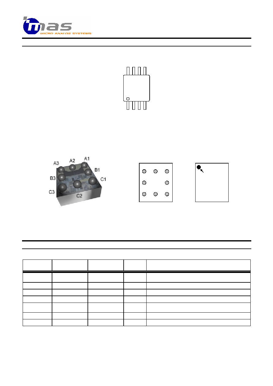
PIN CONFIGURATION
MSOP-8
1
2
3
4
8
7
6
5
For Top Marking Information see
Ordering Information p. 13
WL-CSP
TOP VIEW
BOTTOM VIEW
A1
A2
A3
C1
C2
C3
B3
B1
Pin A1 Designator
For Top Marking Information see
Ordering Information p. 13
PIN DESCRIPTION
Pin Name
Pin Number
in MSOP-8
Pin Number
in WL-CSP
Type
Function
VIN
1, 8
Note 1
A2
P
Power Supply Voltage for Both Regulators
GND
4
C2, C3
G
Ground
CTRL1
3
B3
I
Enable/Disable Pin for the First Regulator
CTRL2
6
B1
I
Enable/Disable Pin for the Second Regulator
TEST
5
C1
I/O
Note 2
Temperature Protection Test Pin
VOUT1
2
A3
O
Output Voltage of the First Regulator
VOUT2
7
A1
O
Output Voltage of the Second Regulator
G = Ground, I = Input, O = Output, P = Power
Note 1:
The pins 1 and 8 in the MSOP-8 package should be connected to each other externally (see the block diagram on page 3).
Note 2:
The TEST pin cannot be loaded.

DA9167.000
8 January 2003
3 (13)
BLOCK DIAGRAM
CTRL1
VIN
VOUT1
VOLTAGE
REFERENCE
+
CTRL2
VIN
VOUT2
GND
OVER TEMPERATURE
PROTECTION
+
OVER CURRENT
PROTECTION
OVER CURRENT
PROTECTION
TEST
ABSOLUTE MAXIMUM RATINGS
All voltages with respect to ground.
Parameter
Symbol
Conditions
Min
Max
Unit
Supply Voltage
V
IN
-0.3
6
V
Voltage Range for All Pins
-0.3
V
IN
+ 0.3
V
ESD Rating
HBM
2
kV
Junction Temperature
T
Jmax
+175
(limited)
∞C
Storage Temperature
T
S
-55
+150
∞C
Stresses beyond those listed may cause permanent damage to the device. The device may not operate under these conditions, but it will
not be destroyed.
RECOMMENDED OPERATING CONDITIONS
All voltages with respect to ground.
Parameter
Symbol
Conditions
Min
Max
Unit
Operating Junction
Temperature
T
J
-40
+125
∞C
Operating Ambient
Temperature
T
A
-40
+85
∞C
V
OUT(NOM)
< 2.2 V
2.5
Operating Supply
Voltage
V
IN
V
OUT(NOM)
2.2 V
V
OUT(NOM)
+ 0.3
5.3
V

DA9167.000
8 January 2003
4 (13)
ELECTRICAL CHARACTERISTICS
Thermal Protection
T
A
= -40∞C to +85∞C, typical values at T
A
= +27∞C, V
IN
= V
OUT(NOM)
+ 1 V, I
OUT
= 1.0 mA, C
IN
= 1 µF, C
L
= 1 µF, V
CTRL
= 2 V, unless
otherwise specified
Parameter
Symbol
Conditions
Min
Typ
Max
Unit
Threshold High
T
H
145
160
175
∞C
Threshold Low
T
L
135
150
165
∞C
The hysteresis of 10∞C prevents the device from turning on too soon after thermal shutdown.
Control Terminal Specifications
T
A
= -40∞C to +85∞C, typical values at T
A
= +27∞C, V
IN
= V
OUT(NOM)
+ 1 V, I
OUT
= 1.0 mA, C
IN
= 1 µF, C
L
= 1 µF, V
CTRL
= 2 V, unless
otherwise specified
Parameter
Symbol
Conditions
Min
Typ
Max
Unit
Control Voltage
OFF State
ON State
V
CTRL
-0.3
1.6
0.55
V
IN
+ 0.3
V
Control Current, one control
input
I
CTRL
V
CTRL
= V
IN
V
CTRL
= 0 V
5
0
15
µA
If CTRL-pin is not connected, the particular regulator is in OFF state (1 M pull-down resistor to ground).
Voltage Parameters
T
A
= -40∞C to +85∞C, typical values at T
A
= +27∞C, V
IN
= V
OUT(NOM)
+ 1 V, I
OUT
= 1.0 mA, C
IN
= 1 µF, C
L
= 1 µF, V
CTRL
= 2 V, unless
otherwise specified
Parameter
Symbol
Conditions
Min
Typ
Max
Unit
Output Voltage Tolerance
V
OUT
I
OUT
= 0 mA
I
OUT
= 150 mA
-1.7
-3.5
+1.7
+1.7
%V
NOM
Operating Supply Voltage
V
IN
V
NOM
+ 0.3
5.3
V
Dropout Voltage
V
DROP
I
OUT
= 1 mA
I
OUT
= 50 mA
I
OUT
= 150 mA
50
70
180
mV
Current Parameters
T
A
= -40∞C to +85∞C, typical values at T
A
= +27∞C, V
IN
= V
OUT(NOM)
+ 1 V, I
OUT
= 1.0 mA, C
IN
= 1 µF, C
L
= 1 µF, V
CTRL
= 2 V, unless
otherwise specified
Parameter
Symbol
Conditions
Min
Typ
Max
Unit
Continuous Output Current
I
OUT
0
150
mA
Short Circuit Current
I
MAX
R
L
= 0
450
mA
Peak Output Current
I
PK
V
OUT
> 95% * V
OUT(NOM)
410
mA
Ground Pin Current
I
GND
one regulator on
I
OUT
= 0 mA
I
OUT
= 10 mA
I
OUT
= 50 mA
I
OUT
= 150 mA
180
220
250
310
µA
Ground Pin Current
I
GND
both regulators on
I
OUT
= 0 mA
I
OUT
= 10 mA
I
OUT
= 50 mA
I
OUT
= 150 mA
250
320
390
510
µA
T
A
= 27∞C
0.03
1
Ground Pin Current, Sleep
Mode
I
GND
V
CTRL1,2
< 0.3 V
T
A
= 85∞C
0.5
5
µA

DA9167.000
8 January 2003
5 (13)
Power Dissipation
T
A
= -40∞C to +85∞C, typical values at T
A
= +27∞C, V
IN
= V
OUT(NOM)
+ 1 V, I
OUT
= 1.0 mA, C
IN
= 1 µF, C
L
= 1 µF, V
CTRL
= 2 V, unless
otherwise specified
Parameter
Symbol
Conditions
Min
Typ
Max
Unit
Junction to Case Thermal
Resistance
R
JC
MSOP-8 package
39
∞C/W
Junction to Ambient Thermal
Resistance
R
JA
typical PC board mounting,
still air, MSOP-8 package
206
∞C/W
Maximum Power Dissipation
P
d
any ambient temperature,
MSOP-8 package
JA
A
(MAX)
J
MAX
d
R
T
T
P
-
=
W
Note 1
Note 1
: T
J(MAX)
denotes maximum operating junction temperature (+125∞C), T
A
ambient temperature, and R
JA
junction-to-ambient thermal
resistance (+206∞C/W).
Line and Load Regulation
T
A
= -40∞C to +85∞C, typical values at T
A
= +27∞C, V
IN
= V
OUT(NOM)
+ 1 V, I
OUT
= 1.0 mA, C
IN
= 1 µF, C
L
= 1 µF, V
CTRL
= 2 V, unless
otherwise specified
Parameter
Symbol
Conditions
Min
Typ
Max
Unit
Line Regulation
V
OUT(NOM)
+ 1 V < V
IN
< 5.3 V,
I
OUT
= 50 mA
1.5
2.5
mV
Load Regulation
I
OUT
= 1.0 to 50 mA
I
OUT
= 1.0 to 150 mA
9
24
20
45
mV
Noise and Ripple Rejection
T
A
= -40∞C to +85∞C, typical values at T
A
= +27∞C, V
IN
= V
OUT(NOM)
+ 1 V, I
OUT
= 1.0 mA, C
IN
= 1 µF, C
L
= 1 µF, V
CTRL
= 2 V, unless
otherwise specified
Parameter
Symbol
Conditions
Min
Typ
Max
Unit
Output Noise Voltage
V
RMS
100 Hz < f < 100 kHz
30
µVrms
Noise Density
V
N
I
OUT
= 50 mA, f = 10 kHz
140
nV
/
Hz
PSRR
I
OUT
= 50 mA
f = 1 kHz
f = 10 kHz
f = 100 kHz
50
40
38
dB