
1 (8)
DA9270.004
4 April, 2002
MAS9270
IC FOR 10.00 ≠ 30.00 MHz VCTCXO
∑
Wide Supply Voltage Range
∑
True Sine Wave Output
∑
Very High Level of Integration
∑
Electrically Trimmable
∑
Very Low Phase Noise
∑
Low Cost
∑
Minimum Operating Temperature ≠40 ∞C
DESCRIPTION
The MAS9270 is an integrated circuit well suited to
build VCTCXO for mobile communication.
Temperature calibration is achieved in three
calibration temperatures only. The trimming is done
through a serial bus and the calibration information
is stored in an internal PROM. This means no
rework for trimming is needed.
To build a VCTCXO additionally only crystal is
required. The compensation method is fully analog,
working continuously without generating any steps
or other interference.
FEATURES
APPLICATIONS
∑
Very small size
∑
Minor current draw
∑
Wide operating temperature range
∑
Phase noise <-120 dBc/Hz at 100Hz offset
∑
Programmable
VC-sensitivity
∑
Minimum Operating Temperature ≠40 ∞C for
MAS9270Cxx3
∑
VCTCXO for mobile phones
∑
VCTCXO for other telecommunications
systems
BLOCK DIAGRAM
T
Vref
TMux
DA
CLK
PV
VSS
VC
VDD
4
4
f(T)
f(T)
4
8
CUB
INF
SENS
LIN
8
CDAC1
CDAC2
TE1
TE2
X2
OUT
X1
2
MAS9270

2 (8)
DA9270.004
4 April, 2002
PIN DESCRIPTION
Pin Description
Symbol
x-coordinate
y-coordinate
Power Supply Voltage
VDD
166
1430
Programming Input
PV
420
1435
Serial Bus Clock Input
CLK
979
1441
Serial Bus Data Input
DA
1234
1441
Temperature Output
TE1
1488
1441
Test Multiplexer Output
TE2
1742
1441
Voltage Control Input
VC
185
153
Crystal Oscillator Output
X1
439
149
Crystal/Varactor Oscillator Input
X2
1357
149
Power Supply Ground
VSS
1790
166
Buffer Output
OUT
2046
153
Note: Because the substrate of the die is internally connected to GND, the die has to be connected to GND or
left floating. Make sure that GND is the first pad to be bonded. Pick-and-place and all component assembly are
recommended to be performed in ESD protected area.
Note: Pad coordinates are measured from the left bottom corner of the chip to the center of the pads. The
coordinates may vary depending on sawing width and location, however, distances between pads are accurate.
ABSOLUTE MAXIMUM RATINGS
Parameter
Symbol
Min
Max
Unit
Note
Supply Voltage
V
DD
- V
SS
-0.3
6.0
V
Input Pin Voltage
V
SS
-0.3
V
DD
+ 0.3
V
1)
Power Dissipation
P
MAX
20
mW
Storage Temperature
T
ST
-45
120
o
C
Note 1: Not valid for programming pin PV
RECOMMENDED OPERATION CONDITIONS
Parameter
Symbol
Conditions
Min
Typ
Max
Unit
Note
Supply Voltage
V
DD
2.7
2.8
5.5
V
1)
Supply Current
I
CC
Vdd = 2.8 Volt
1.8
mA
Operating Temperature
T
OP
-30
+85
o
C
2)
Storage Temperature
T
S
Relative humidity =
15%...70%
-45
+40
o
C
Crystal Pulling Sensitivity
S
30
ppm/pF
Crystal Load Capacitance
C
L
10
pF
Note 1: Minimum Supply Voltage 2.6 V for MAS9270Cxx2 version.
Note 2: Minimum Operating Temperature ≠40 ∞C for MAS9270Cxx3 version.
3 (8)
DA9270.004
4 April, 2002
ELECTRICAL CHARACTERISTICS
(recommended operation conditions)
Parameter
Symbol
Min
Typ
Max
Unit
Note
Frequency Range
f
o
10.00
30.00
MHz
Voltage Control Range
V
C
0
Vdd
V
Voltage Control Sensitivity (VCR = 0)
V
CSENS
9
15
ppm/V
1)
Voltage Control Sensitivity (VCR = 1)
V
CSENS
4
8
ppm/V
Output Voltage (10k
// 10 pF)
V
out
1.0
Vpp
Compensation Range ± 2.5 ppm
T
C
-30
85
o
C
Compensation Range ± 2.0 ppm
T
C
-25
75
o
C
Compensation Range ± 2.5 ppm
T
C
-40
85
o
C
4)
Compensation Range Linear Part
a1
-0.7
0.0
ppm/K
Compensation Inflection Point
INF
25
31
o
C
Compensation Range Cubic Part
a3
95
ppm
2
/K
3
Compensation CDAC1 (7 Bit)
C
X1
C10
C10 + 18
pF
2)
Compensation CDAC2 (2 Bit)
C
X2
C20
C20 + 4
pF
3)
Start up Time
T
START
2
ms
Note 1: default
Note 2: typ C10 = 13 pF
Note 3: typ C20 = 6 pF (varactor capacitance at 1.8 V 12 pF)
Note 4: MAS9270Cxx3
IC OUTLINES
Note 1: MAS9270 pads are round with 80 µm diameter at opening.
Note 2: Pins CLK and DA can either be connected to VSS or left floating, pin PV can either be connected to
VDD or left floating and pin TE1 must be left floating in VCTCXO module end-user application.
Note 3: Die map reference is the actual left bottom corner of the sawn chip.
VDD
PV
CLK
DA
TE1
TE2
VC
X1
X2
VSS
OUT
MAS9270
2204 µm
1
5
8
4
µ
m
Die map reference

4 (8)
DA9270.004
4 April, 2002
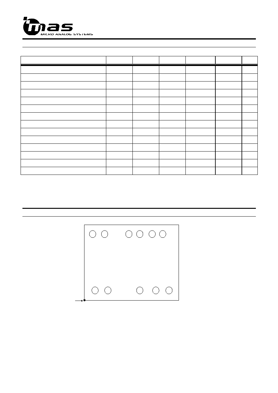
SAMPLES IN SB20 DIL PACKAGE
DEVICE OUTLINE CONFIGURATION
M
A
S
9
2
7
0
Y
Y
W
W
X
X
X
X
X
.
X
2
1
20
3
4
5
6
7
8
9
10
19
18
17
16
15
14
13
12
11
VC
X1
GND
X2
OUT
VDD
DA
CLK
PV
Top marking:
YYWW = Year, Week
XXXXX.X = Lot number
TE2
TE1
MSOP10
TE2
DA
CLK
PV
VDD
OUT
VSS
X2
X1
VC
Top View
9
2
7
0
C
X
Y
W
W
C = product version
X = voltage version
Y = year
WW= week
5 (8)
DA9270.004
4 April, 2002
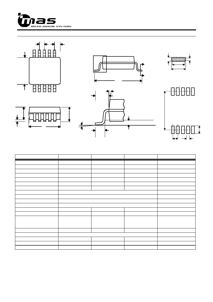
PACKAGE (MSOP-10) OUTLINE
Symbol
Min
Nom
Max
Unit
A
--
--
1.10
mm
A1
0.00
--
0.15
mm
A2
0.75
0.85
0.95
mm
b
0.15
--
0.30
mm
b1
0.15
---
0.25
mm
c
0.08
0.23
mm
c1
0.08
0.18
mm
D
3.00 BSC
mm
E
4.90 BSC
mm
E1
3.00 BSC
mm
e
0.50 BSC
mm
F
4.8
mm
G
0.50
mm
L
(Terminal length for
soldering)
0.40
0.60
0.80
mm
L1
0.95 REF
L2
0.25 BSC
mm
M
0.41
mm
N
1.02
mm
S
0.50
Mm
Dimensions do not include mold or interlead flash, protrusions or gate burrs.
Reference Standard : JEDEC MO-187 BA.
b1
B
(b)
c
c1
F
G
M
N
Land
Pattern
Recommendation
See Detail A
Detail A
5-15 Degrees
Gauge Plane
Seating Plane
0 - 8 Degrees
B
E
L1
L
L2
D
A
A1
E1
e
S
E1
A2
E
A
A
Section B - B