DA9278.002
29 January 2003
1 (5)
MAS9278
IC for 10.00 ≠ 30.00 MHz VCXO
∑
Low Power
∑
Wide Supply Voltage Range
∑
True Sine Wave Output
∑
Very High Level of Integration
∑
Integrated Varactor
∑
Electrically Trimmable
∑
Very Low Phase Noise
∑
Low Cost
DESCRIPTION
The MAS9278 is an integrated circuit well suited to
build VCXO for mobile communication. The crystal
offset trimming is done through a serial bus and the
calibration information is stored in an internal
PROM.
To build a VCXO only one additional component, a
crystal, is needed.
FEATURES
APPLICATIONS
∑
Very small size
∑
Minor current draw
∑
Wide operating temperature range
∑
Phase noise <-130 dBc/Hz at 1 kHz offset
∑
Programmable Vc sensitivity
∑
VCXO for mobile phones
∑
VCXO for other telecommunications systems
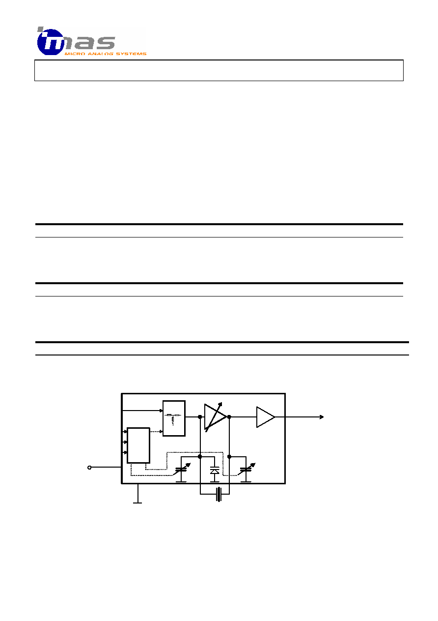
BLOCK DIAGRAM
DA
CLK
PV
VSS
VC
VDD
X2
OUT
X1
XO1
Digital
MAS9278
5
2
2
DA9278.002
29 January 2003
2 (5)
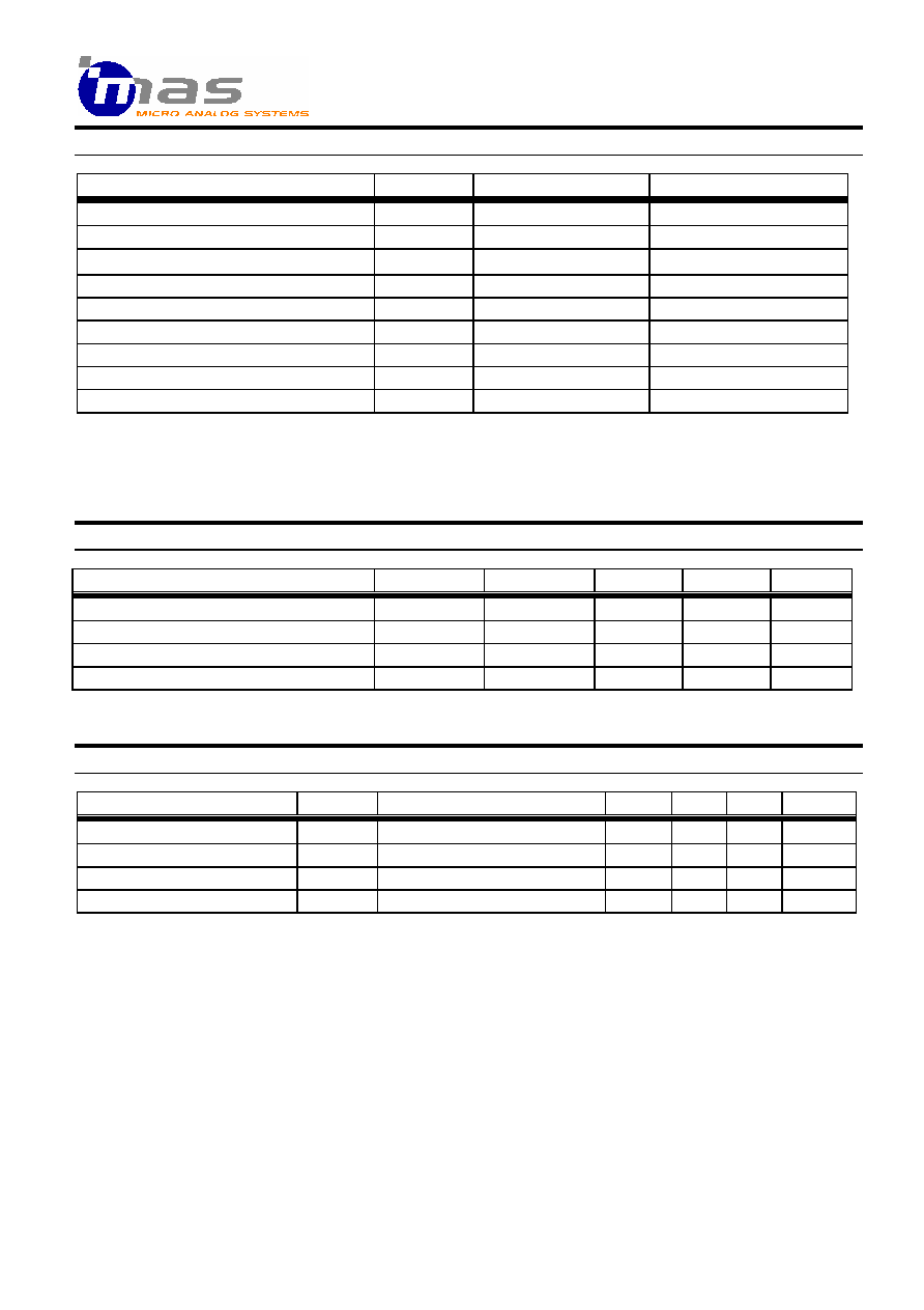
PIN DESCRIPTION
Pin Description
Symbol
x-coordinate
y-coordinate
Power Supply Voltage
VDD
177
172
Serial Bus Data Input
DA
435
1015
Serial Bus Clock Input
CLK
201
1015
Programming Input
PV
1042
1015
Voltage Control Input
VC
1012
158
Crystal Oscillator Output
X1
374
158
Power Supply Ground
VSS
830
1008
Crystal/Varactor Oscillator Input
X2
817
158
Buffer Output
OUT
665
1015
Note: Because the substrate of the die is internally connected to GND, the die has to be connected to GND or
left floating. Make sure that GND is the first pad to be bonded. Pick-and-place and all component assembly are
recommended to be performed in ESD protected area.
Note: Pad coordinates are measured from the left bottom corner of the chip to the center of the pads. The
coordinates may vary depending on sawing width and location, however, distances between pads are accurate.
ABSOLUTE MAXIMUM RATINGS
Parameter
Symbol
Min
Max
Unit
Note
Supply Voltage
V
DD
- V
SS
-0.3
6.0
V
Input Voltage
V
IN
V
SS
-0.3
V
DD
+ 0.3
V
1)
Power Dissipation
P
MAX
20
mW
Storage Temperature
T
ST
-40
120
o
C
Note: Not valid for programming pin PV.
RECOMMENDED OPERATION CONDITIONS
Parameter
Symbol
Conditions
Min
Typ
Max
Unit
Supply Voltage
V
DD
2.7
2.8
5.5
V
Supply Current
I
CC
Vcc = 2.8 Volt
0.85
mA
Operating Temperature
T
C
-30
+85
o
C
Crystal Load Capacitance
C
L
7.0
pF
DA9278.002
29 January 2003
3 (5)
ELECTRICAL CHARACTERISTICS
(recommended operation conditions)
Parameter
Symbol
Min
Typ
Max
Unit
Note
Frequency Range
f
o
10.00
30.00
MHz
Voltage Control Range
V
C
0
Vdd
Voltage Control Sensitivity
V
CSENS
15..30
ppm/V
1)
Output Voltage (10k
// 10 pF)
V
out
1.0
Vpp
Compensation CDAC1 (2 Bit)
C
X1
C10
C10 + 4.5
pF
2)
Compensation CDAC2 (4 Bit)
C
X2
C20
C20 + 18
pF
3)
Startup Time
T
START
2
ms
Note 1: programmable by DN/DP switches
Note 2: typ C10 = 4.5 pF
Note 3: typ C20 = 12.5 pF
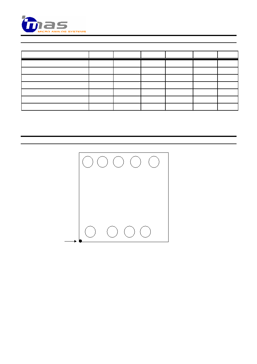
IC OUTLINES
Note 1: MAS9278 pads are round with 80 µm diameter at opening.
Note 2: Pins CLK and DA can either be connected to VSS or left floating and pin PV can either be connected to
VDD or left floating in VCXO module end-user application.
Note 3: Die map reference is the actual left bottom corner of the sawn chip.
1200 µm
1
1
8
2
µ
m
Die map reference
VDD
CLK
PV
OUT
X2
VSS
X1
VC
MAS9278
DA
DA9278.002
29 January 2003
4 (5)
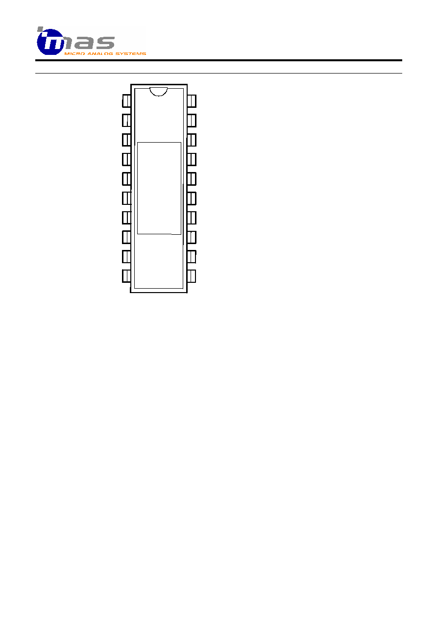
SAMPLES IN SB20 DIL PACKAGE
M
A
S
9
2
7
8
Y
Y
W
W
X
X
X
X
X
.
X
2
1
20
3
4
5
6
7
8
9
10
19
18
17
16
15
14
13
12
11
VC
X1
GND
X2
OUT
VDD
DA
CLK
PV
Top marking:
YYWW = Year, Week
XXXXX.X = Lot number
DA9278.002
29 January 2003
5 (5)
ORDERING INFORMATION
Product Code
Product
Package
Comments
MAS9278ATG1
IC FOR VCXO
EWS tested wafers 215 µm
Die Size 1.200 x 1.182 mm
MAS9278
IC FOR VCXO
SMD Package T.B.D.
Please contact Micro Analog Systems Oy for other wafer thickness options.
LOCAL DISTRIBUTOR
MICRO ANALOG SYSTEMS OY CONTACTS
Micro Analog Systems Oy
Kamreerintie 2, P.O. Box 51
FIN-02771 Espoo, FINLAND
http://
www.mas-oy.com
Tel. (09) 80 521
Tel. Int. +358 9 80 521
Telefax +358 9 805 3213
Email: info@mas-oy.com
NOTICE
Micro Analog Systems Oy reserves the right to make changes to the products contained in this data sheet in order to improve the design or
performance and to supply the best possible products. Micro Analog Systems Oy assumes no responsibility for the use of any circuits
shown in this data sheet, conveys no license under any patent or other rights unless otherwise specified in this data sheet, and makes no
claim that the circuits are free from patent infringement. Applications for any devices shown in this data sheet are for illustration only and
Micro Analog Systems Oy makes no claim or warranty that such applications will be suitable for the use specified without further testing or
modification.