 | –≠–ª–µ–∫—Ç—Ä–æ–Ω–Ω—ã–π –∫–æ–º–ø–æ–Ω–µ–Ω—Ç: 4066 | –°–∫–∞—á–∞—Ç—å:  PDF PDF  ZIP ZIP |
_______________General Description
The MAX4066/MAX4066A quad, SPST, CMOS analog
switches are designed to provide superior performance
over the industry-standard devices. These new switch-
es feature guaranteed operation from +2.0V to +16V
and are fully specified at 3V, 5V, and 12V. Both parts
offer 45
on-resistance and 2
channel-to-channel
matching at 12V, plus 4
flatness over the specified
signal range.
Each device is controlled by TTL/CMOS input levels
and can be used as a bilateral switch or multiplexer/
demultiplexer.
Low off leakage current (100pA for the MAX4066A) and
low power consumption (0.5µW) make the MAX4066/
MAX4066A ideal for battery-operated equipment. These
parts are also suitable for low-distortion audio applica-
tions. Both devices are available in 14-pin DIP and SO
packages, as well as a 16-pin QSOP. ESD protection is
greater than 2000V per Method 3015.7.
________________________Applications
Battery-Operated Equipment
Audio and Video Signal Routing
Low-Voltage Data-Acquisition Systems
Sample-and-Hold Circuits
Communication Circuits
____________________________Features
o
Pin Compatible with 74HC4066
o
Guaranteed On-Resistance:
170
max (3V supply)
45
max (12V supply)
o
Guaranteed Match Between Channels:
4
max (MAX4066)
2
max (MAX4066A)
o
Guaranteed Low Leakage Currents:
1nA at +25∞C (MAX4066)
100pA at +25∞C (MAX4066A)
o
Single-Supply Operation from +2.0V to +16V
o
V+ to GND Signal Handling
o
TTL/CMOS-Logic Compatible
o
Low Power Consumption: 0.5µW
o
Low Crosstalk: -86dB
o
Low Off Isolation: -58dB
o
Low Distortion: 0.03%
o
Wide Bandwidth: > 100MHz
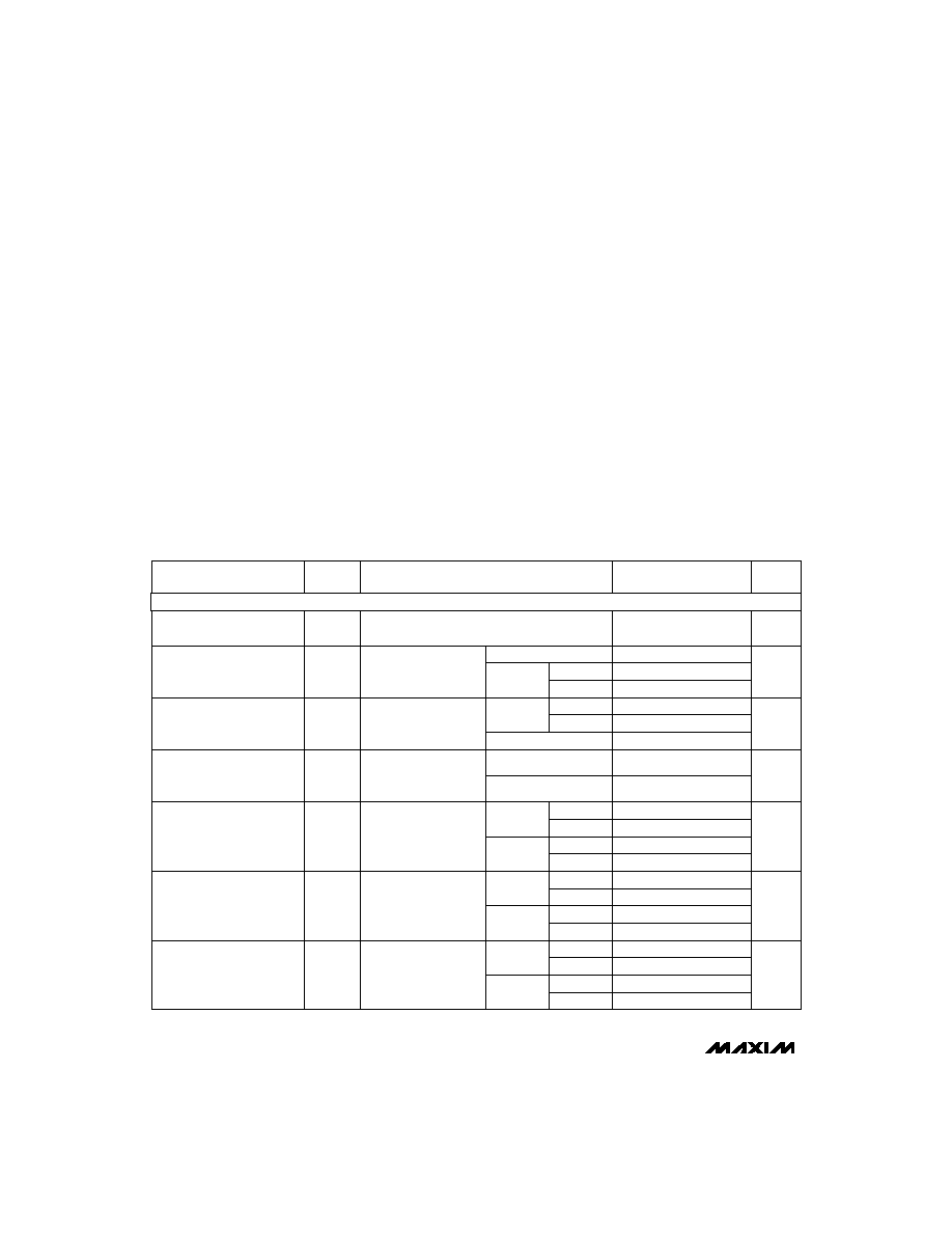
MAX4066/MAX4066A
Low-Cost, Low-Voltage, Quad, SPST,
CMOS Analog Switches
14
13
12
11
10
9
8
1
2
3
4
5
6
7
V+
TRUTH TABLE
ON/OFF CONTROL
INPUT
L
H
OFF
ON
STATE OF
ANALOG SWITCH
IN1
IN4
NO4
COM2
NO2
COM1
NO1
TOP VIEW
MAX4066
MAX4066A
COM4
COM3
NO3
GND
IN3
IN2
DIP/SO
16
15
14
13
12
11
10
9
1
2
3
4
5
6
7
8
V+
IN1
IN4
NO4
COM4
N.C.
COM3
NO3
NO1
COM1
N.C.
NO2
COM2
IN2
IN3
GND
MAX4066
MAX4066A
QSOP
N.C. = NO INTERNAL CONNECTION
______________________________________________Pin Configurations/Truth Table
19-0439; Rev 1; 3/96
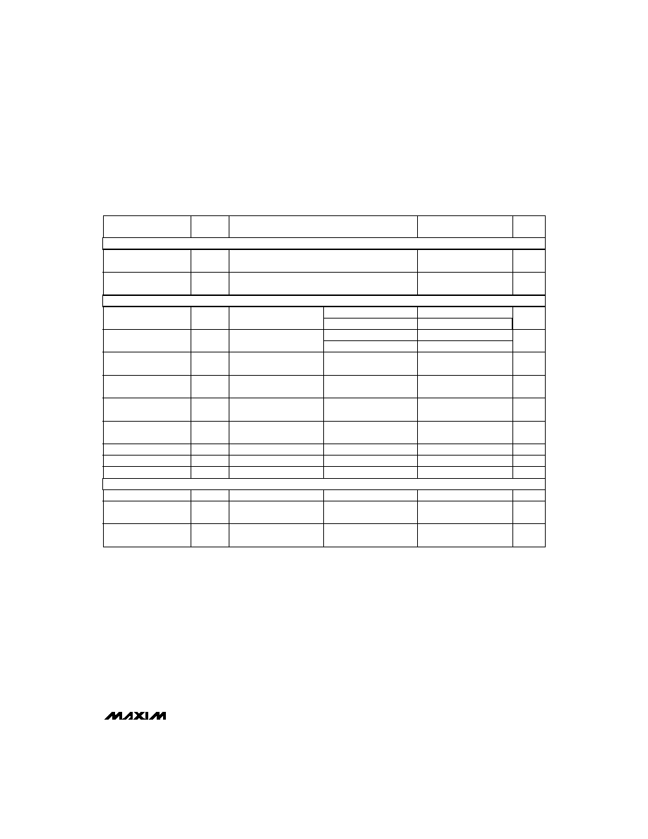
PART
MAX4066
CPD
MAX4066CSD
MAX4066CEE
0∞C to +70∞C
0∞C to +70∞C
0∞C to +70∞C
TEMP. RANGE
PIN-PACKAGE
14 Plastic DIP
14 Narrow SO
16 QSOP
______________Ordering Information
Ordering Information continued at end of data sheet.
* Contact factory for dice specifications.
MAX4066C/D
0∞C to +70∞C
Dice*
________________________________________________________________
Maxim Integrated Products
1
For free samples & the latest literature: http://www.maxim-ic.com, or phone 1-800-998-8800
MAX4066/MAX4066A
Low-Cost, Low-Voltage, Quad, SPST,
CMOS Analog Switches
2
_______________________________________________________________________________________
ABSOLUTE MAXIMUM RATINGS
ELECTRICAL CHARACTERISTICS--Single +12V Supply
(V+ = 12V ±10%, GND = 0V, V
INH
= 4.0V, V
INL
= 0.8V, T
A
= T
MIN
to T
MAX
, unless otherwise noted.)
Stresses beyond those listed under "Absolute Maximum Ratings" may cause permanent damage to the device. These are stress ratings only, and functional
operation of the device at these or any other conditions beyond those indicated in the operational sections of the specifications is not implied. Exposure to
absolute maximum rating conditions for extended periods may affect device reliability.
(Voltages referenced to GND)
V+ ...........................................................................-0.3V to +17V
V
IN_
, V
COM_
, V
NO
(Note 1) ...........................-0.3V to (V + +0.3V)
Current (any terminal) .........................................................30mA
Peak Current (any terminal) ..............................................100mA
ESD per Method 3015.7 ..................................................>2000V
Continuous Power Dissipation (T
A
= +70∞C)
Plastic DIP (derate 10.00mW/∞C above +70∞C) ............800mW
Narrow SO (derate 8.00mW/∞C above +70∞C) ..............640mW
QSOP (derate 9.52mW/∞C above +70∞C) ......................762mW
CERDIP (derate 9.09mW/∞C above +70∞C) ....................727mW
Operating Temperature Ranges
MAX4066C_ _/MAX4066AC_ _ .............................0∞C to +70∞C
MAX4066E_ _/MAX4066AE_ _...........................-40∞C to +85∞C
MAX4066MJD/MAX4066AMJD .......................-55∞C to +125∞C
Storage Temperature Range .............................-65∞C to +150∞C
Lead Temperature (soldering, 10sec) .............................+300∞C
(Note 3)
V+ = 12V,
V
COM
= 0V,
V
NO
= 10V
V+ = 12V,
I
COM
= 2mA,
V
NO
= 10V
V+ = 12V,
I
COM
= 2mA,
V
NO
= 10V, 5V, 1V
CONDITIONS
nA
-100
100
I
NO(OFF)
NO or NC Off Leakage
Current (Note 6)
-6
6
-0.1
0.1
-1
1
6
R
FLAT(ON)
On-Resistance Flatness
(Note 5)
V
0
V+
V
COM
,
V
NO
Analog Signal Range
2
4
6
R
ON
On-Resistance Match
Between Channels (Note 4)
0.5
2
0.5
4
16
45
UNITS
MIN
TYP
MAX
(Note 2)
SYMBOL
PARAMETER
T
A
= +25∞C
MAX4066
MAX4066A
T
A
= +25∞C
T
A
= T
MIN
to T
MAX
T
A
= +25∞C
T
A
= T
MIN
to T
MAX
T
A
= +25∞C
T
A
= T
MIN
to T
MAX
MAX4066
MAX4066A
C, E
M
V+ = 12V,
V
COM
= 0V,
V
NO
= 10V
T
A
= +25∞C
nA
-100
100
I
COM(OFF)
COM Off Leakage Current
(Note 6)
-6
6
T
A
= T
MIN
to T
MAX
MAX4066
-0.1
0.1
MAX4066A
C, E
-1
1
M
V+ = 12V,
V
COM
= 10V,
V
NO
= 10V
T
A
= +25∞C
nA
-200
200
I
COM(ON)
COM On Leakage Current
(Note 6)
-12
12
T
A
= T
MIN
to T
MAX
MAX4066
-0.2
0.2
MAX4066A
C, E
-2
2
M
C, E
55
M
On-Resistance
R
ON
V+ = 12V,
I
COM
= 2mA,
V
NO
= 10V
T
A
= T
MIN
to T
MAX
75
Note 1:
Signals on NO_, COM_, or IN_ exceeding V+ or GND are clamped by internal diodes. Limit forward-diode current to
maximum current rating.
ANALOG SWITCH
MAX4066/MAX4066A
Low-Cost, Low-Voltage, Quad, SPST,
CMOS Analog Switches
_______________________________________________________________________________________
3
ELECTRICAL CHARACTERISTICS--Single +12V Supply (continued)
(V+ = 12V ±10%, GND = 0V, V
INH
= 4.0V, V
INL
= 0.8V, T
A
= T
MIN
to T
MAX
, unless otherwise noted.)
PARAMETER
SYMBOL
MIN
TYP
MAX
(Note 2)
UNITS
Input Current with Input
Voltage High
I
INH
-0.5
0.005
0.5
µA
CONDITIONS
IN = 5.0V, all others = 0.8V
Input Current with Input
Voltage Low
I
INL
-0.5
0.005
0.5
µA
IN = 0.8V, all others = 5.0V
Turn-On Time
t
ON
25
100
ns
Charge Injection
(Note 3)
V
CTE
1
10
pC
C
L
= 1.0nF, V
GEN
= 0V,
R
GEN
= 0
, Figure 3
T
A
= +25∞C
T
A
= T
MIN
to T
MAX
150
V
COM
= 10V, Figure 2
T
A
= +25∞C
T
A
= T
MIN
to T
MAX
100
V
COM
= 10V, Figure 2
Turn-Off Time
t
OFF
15
75
ns
Power-Supply Range
Signal = 0dbm, Figure 4,
50
in and out
On-Channel Bandwidth
BW
100
MHz
T
A
= +25∞C
T
A
= +25∞C
R
L
= 50
, C
L
= 5pF,
f = 1MHz, Figure 4
Off Isolation (Note 7)
V
ISO
-58
dB
T
A
= +25∞C
R
L
= 50
, C
L
= 5pF,
f = 1MHz, Figure 5
Crosstalk (Note 8)
V
CT
-86
dB
T
A
= +25∞C
f = 1MHz, Figure 6
NO Capacitance
C
(OFF)
9
pF
T
A
= +25∞C
f = 1MHz, Figure 6
COM Off Capacitance
C
COM(OFF)
9
pF
T
A
= +25∞C
f = 1MHz, Figure 6
COM On Capacitance
C
COM(ON)
pF
V
Supply Current
22
I+
V
IN
= 0V or V+,
all channels on or off
T
A
= T
MIN
to T
MAX
-1
0.001
1
µA
Total Harmonic
Distortion
THD
T
A
= T
MIN
to T
MAX
0.03
%
T
A
= +25∞C
LOGIC INPUT
SUPPLY
DYNAMIC

MAX4066/MAX4066A
Low-Cost, Low-Voltage, Quad, SPST,
CMOS Analog Switches
4
_______________________________________________________________________________________
PARAMETER
SYMBOL
MIN
TYP
MAX
(Note 2)
UNITS
Analog Signal Range
V
COM,
V
NO
0
V+
V
CONDITIONS
(Note 3)
On-Resistance
R
ON
45
75
V+ = 4.5V,
I
COM
= -1.0mA,
V
NO
= 3.5V
Turn-On Time
t
ON
43
125
ns
V
NO
= 3V
On-Channel
Bandwidth
BW
100
MHz
Signal = 0dBm,
50
in and out, Figure 4
Turn-Off Time
t
OFF
18
75
ns
V
NO
= 3V
Positive Supply Current
I+
-1
1
µA
Charge Injection
(Note 3)
Q
2
10
pC
V
GEN
= 0V, R
GEN
= 0V,
C
L
= 1.0nF, Figure 3
T
A
= +25∞C
T
A
= +25∞C
T
A
= +25∞C
T
A
= +25∞C
T
A
= +25∞C
T
A
= +25∞C
T
A
= T
MIN
to T
MAX
T
A
= T
MIN
to T
MAX
-100
100
On-Resistance Match
Between Channels (Note 4)
R
ON
0.3
4
V+ = 5V,
I
COM
= -1.0mA,
V
NO
= 3V
On-Resistance Flatness
(Notes 3, 5)
R
FLAT(ON)
4
6
V+ = 5V,
I
COM
= -1.0mA,
V
NO
= 1V, 3V
NO Off Leakage
Current (Note 6)
I
NO(OFF)
-1
1
nA
V+ = 5.5V,
V
COM
= 0V,
V
NO
= 4.5V
COM Off Leakage Current
(Note 6)
I
COM(OFF)
-1
1
nA
V+ = 5.5V,
V
COM
= 0V,
V
NO
= 4.5V
COM On Leakage Current
(Note 6)
I
COM(ON)
-2
2
nA
V+ = 5.5V,
V
COM
= 5V,
V
NO
= 4.5V
-6
6
-200
200
52
100
12
8
-6
6
-100
100
T
A
= T
MIN
to T
MAX
T
A
= T
MIN
to T
MAX
T
A
= T
MIN
to T
MAX
C, E
M
C, E
M
C, E
M
-12
12
T
A
= +25∞C
T
A
= +25∞C
T
A
= T
MIN
to T
MAX
T
A
= T
MIN
to T
MAX
175
125
T
A
= +25∞C
V+ = 5.5V, V
IN
= 0V or V+, all channels on or off
ELECTRICAL CHARACTERISTICS--Single +5V Supply
(V+ = 5V ±10%, V- = 0V ±10%, GND = 0V, V
INH
= 2.4V, V
INL
= 0.8V, T
A
= T
MIN
to T
MAX
, unless otherwise noted.)
125
T
A
= T
MIN
to T
MAX
ANALOG SWITCH
DYNAMIC
SUPPLY
C, E
M
MAX4066
MAX4066A
MAX4066
MAX4066A
MAX4066
MAX4066A
-0.1
0.1
-0.2
0.2
-0.1
0.1
MAX4066/MAX4066A
Low-Cost, Low-Voltage, Quad, SPST,
CMOS Analog Switches
_______________________________________________________________________________________
5
PARAMETER
SYMBOL
MIN
TYP
MAX
(Note 2)
UNITS
Analog Signal Range
V
COM,
V
NO
0
V+
V
CONDITIONS
(Note 3)
Channel On-Resistance
R
ON
170
V+ = 3V,
I
COM
= -1.0mA,
V
NO
= 1.5V
Turn-On Time (Note 3)
t
ON
80
185
ns
V+ = 3V,
V
NO
or V
NC
= 1.5V
Turn-Off Time (Note 3)
t
OFF
28
150
ns
V+ = 3V,
V
NO
or V
NC
= 1.5V
Positive Supply Current
I+
-1
0.001
1
µA
Charge Injection (Note 3)
Q
2
10
pC
C
L
= 1.0nF,
V
GEN
= 0V, R
GEN
= 0V
V+ = 3.6V, V
IN
= 0V or V+, all channels on or off
T
A
= +25∞C
T
A
= +25∞C
T
A
= +25∞C
T
A
= +25∞C
T
A
= T
MIN
to T
MAX
T
A
= T
MIN
to T
MAX
T
A
= T
MIN
to T
MAX
225
230
200
ANALOG SWITCH
DYNAMIC
SUPPLY
Note 2:
The algebraic convention, where the most negative value is a minimum and the most positive value a maximum, is used in
this data sheet.
Note 3:
Guaranteed by design.
Note 4:
R
ON
= R
ON
(max) - R
ON
(min).
Note 5:
Flatness is defined as the difference between the maximum and minimum value of on-resistance as measured over the
specified analog signal range.
Note 6:
Leakage parameters are 100% tested at maximum-rated hot temperature and guaranteed by correlation at +25∞C.
Note 7:
Off Isolation = 20log
10
(V
COM
/ V
NO
), V
COM
= output, V
NO
= input to off switch.
Note 8:
Between any two switches.
ELECTRICAL CHARACTERISTICS--Single +3V Supply
(V+ = 2.7V to 3.3V ±10%, GND = 0V, V
INH
= 2.4V, V
INL
= 0.8V, T
A
= T
MIN
to T
MAX
, unless otherwise noted.)