 | –≠–ª–µ–∫—Ç—Ä–æ–Ω–Ω—ã–π –∫–æ–º–ø–æ–Ω–µ–Ω—Ç: 4206K | –°–∫–∞—á–∞—Ç—å:  PDF PDF  ZIP ZIP |

________________________________
MAX6964
I
2
C
TM
17-
.
50mA
7V
.
LED
7V
.
8
PWM
. 4-
LED
14
.
4-
16
.
8
.
. LED
.
BLINK
(
1kHz)
. BLINK
LED
(GPI)
.
MAX6964
2-
I
2
C
, 4
I
2
C
.
________________________________
________________________________
400kbps, 2-
, 5.5V
2V~3.6V
8-
PWM LED
16
16
2-
LED
--
50mA (
)
RST
7V
(1.2µA (
)
3.3µA (
))
4mm x 4mm, 0.8mm
QFN
-40∞C~+125∞C
MAX6964
17-
LED
/GPO
________________________________________________________________ Maxim Integrated Products
1
RST
AD0
V+
SDA
O10
O4
O3
O2
O1
O0
BLINK
1
2
3
4
5
6
19
20
21
22
23
24
SCL
O15
O14
O13
O12
O11
O9
O8
O7
O6
O5
GND
18
17
16
15
14
13
7
8
9
10
11
12
O16
TOP VIEW
QFN
MAX6964
_________________________________
MAX6964
O8
O10
O0
O1
O2
O3
O4
O5
O6
O7
V+
3.3V
µC
SDA
SCL
SDA
I/O
I/O
AD0
5V
3.3V
6V
O11
O12
O13
O14
O15
SCL
O9
OUTPUT
OUTPUT
RELAY
RELAY
GND
7V
0.047
µF
RST
BLINK
O16
RELAY
________________________
19-3179; Rev 0; 1/04
For pricing, delivery, and ordering information, please contact Maxim/Dallas Direct! at
1-888-629-4642, or visit Maxim's website at www.maxim-ic.com.
________________________________
PART
TEMP RANGE
PIN-PACKAGE
MAX6964ATG
-40
∞C to +125∞C
24 Thin QFN
4mm x 4mm x 0.8mm
MAX6964AEG
-40
∞C to +125∞C
24 QSOP
Pin Configurations continued at end of data sheet.
LCD
LED
RGB LED
Maxim Integrated Products
I
2
C
I
2
C
I
2
C
.
I
2
C
.

MAX6964
17-
LED
/GPO
2
_______________________________________________________________________________________
ABSOLUTE MAXIMUM RATINGS
Stresses beyond those listed under "Absolute Maximum Ratings" may cause permanent damage to the device. These are stress ratings only, and functional
operation of the device at these or any other conditions beyond those indicated in the operational sections of the specifications is not implied. Exposure to
absolute maximum rating conditions for extended periods may affect device reliability.
Voltage (with respect to GND)
V+ .............................................................................-0.3V to +4V
SCL, SDA, AD0, BLINK, RST ...................................-0.3V to +6V
O0≠O16 ....................................................................-0.3V to +8V
DC Current on O0 to O16 ...................................................55mA
DC Current on SDA.............................................................10mA
Maximum GND Current ....................................................350mA
Continuous Power Dissipation (T
A
= +70∞C)
24-Pin QSOP (derate 9.5mW/∞C over +70∞C)..............761mW
24-Pin QFN (derate 20.8mW/∞C over +70∞C) ............1666mW
Operating Temperature Range .........................-40∞C to +125∞C
Junction Temperature ......................................................+150∞C
Storage Temperature Range .............................-65∞C to +150∞C
Lead Temperature (soldering, 10s) .................................+300∞C
ELECTRICAL CHARACTERISTICS
(Typical Operating Circuit, V+ = 2V to 3.6V, T
A
= T
MIN
to T
MAX
, unless otherwise noted. Typical values are at V+ = 3.3V, T
A
= +25∞C.)
(Note 1)
PARAMETER
SYMBOL
CONDITIONS
MIN
TYP
MAX
UNITS
Operating Supply Voltage
V+
2.0
3.6
V
Output Load External Supply
Voltage
V
EXT
0
7
V
T
A
= +25∞C
1.2
2.3
T
A
= -40∞C to +85∞C
2.6
Standby Current
(Interface Idle, PWM Disabled)
I
+
S C L and S D A at V + ; other
d i g i tal i np uts at V + or GN D ;
P WM i ntensi ty contr ol d i sab l ed
T
A
= T
MIN
to T
MAX
3.3
µA
T
A
= +25∞C
8.5
15.1
T
A
= -40∞C to +85∞C
16.5
Supply Current
(Interface Idle, PWM Enabled)
I
+
S C L and S D A at V + ; other
d i g i tal i np uts at V + or GN D ;
P WM i ntensi ty contr ol d i sab l ed
T
A
= T
MIN
to T
MAX
17.2
µA
T
A
= +25∞C
50
95.3
T
A
= -40∞C to +85∞C
99.2
Supply Current
(Interface Running, PWM
Disabled)
I
+
f
SCL
= 400kHz; other digital
inputs at V+ or GND; PWM
intensity control enabled
T
A
= T
MIN
to T
MAX
102.4
µA
T
A
= +25∞C
57
110.2
T
A
= -40∞C to +85∞C
117.4
Supply Current
(Interface Running, PWM
Enabled)
I
+
f
SCL
= 400kHz; other digital
inputs at V+ or GND; PWM
intensity control enabled
T
A
= T
MIN
to T
MAX
122.1
µA
Input High Voltage
SDA, SCL, AD0, BLINK,
RST
V
IH
0.7 x
V+
V
Input Low Voltage
SDA, SCL, AD0, BLINK,
RST
V
IL
0.3 x
V+
V
Input Leakage Current
SDA, SCL, AD0, BLINK,
RST
I
IH
, I
IL
0
input voltage 5.5V
-0.2
+0.2
µA
Input Capacitance
SDA, SCL, AD0, BLINK,
RST
8
pF
MAX6964
17-
LED
/GPO
_______________________________________________________________________________________
3
ELECTRICAL CHARACTERISTICS (continued)
(Typical Operating Circuit, V+ = 2V to 3.6V, T
A
= T
MIN
to T
MAX
, unless otherwise noted. Typical values are at V+ = 3.3V, T
A
= + 25∞C.)
(Note 1)
PARAMETER
SYMBOL
CONDITIONS
MIN
TYP
MAX
UNITS
T
A
= +25∞C
0.15
0.26
T
A
= -40∞C to +85∞C
0.3
V+ = 2V, I
SINK
= 20mA
T
A
= T
MIN
to T
MAX
0.32
V
T
A
= +25∞C
0.13
0.23
T
A
= -40∞C to +85∞C
0.26
V+ = 2.5V, I
SINK
= 20mA
T
A
= T
MIN
to T
MAX
0.28
V
T
A
= +25∞C
0.12
0.23
T
A
= -40∞C to +85∞C
0.24
Output Low Voltage
O0≠O16
V
OL
V+ = 3.3V, I
SINK
= 20mA
T
A
= T
MIN
to T
MAX
0.26
V
Output Low-Voltage SDA
V
OLSDA
I
SINK
= 6mA
0.4
V
PWM Clock Frequency
f
PWM
32
kHz
TIMING CHARACTERISTICS
(Typical Operating Circuit, V+ = 2V to 3.6V, T
A
= T
MIN
to T
MAX
, unless otherwise noted. Typical values are at V+ = 3.3V, T
A
= +25∞C.)
(Note 1)
PARAMETER
SYMBOL
CONDITIONS
MIN
TYP
MAX
UNITS
Serial Clock Frequency
f
SCL
400
kHz
Bus Free Time Between a STOP and a START
Condition
t
BUF
1.3
µs
Hold Time, Repeated START Condition
t
HD, STA
0.6
µs
Repeated START Condition Setup Time
t
SU, STA
0.6
µs
STOP Condition Setup Time
t
SU, STO
0.6
µs
Data Hold Time
t
HD, DAT
(Note 2)
0.9
µs
Data Setup Time
t
SU, DAT
180
ns
SCL Clock Low Period
t
LOW
1.3
µs
SCL Clock High Period
t
HIGH
0.7
µs
Rise Time of Both SDA and SCL Signals, Receiving
t
R
(Notes 3, 4)
20 +
0.1C
b
300
ns
Fall Time of Both SDA and SCL Signals, Receiving
t
F
(Notes 3, 4)
20 +
0.1C
b
300
ns
Fall Time of SDA Transmitting
t
F.TX
(Notes 3, 5)
20 +
0.1C
b
250
ns
Pulse Width of Spike Suppressed
t
SP
(Note 6)
50
ns
MAX6964
17-
LED
/GPO
4
_______________________________________________________________________________________
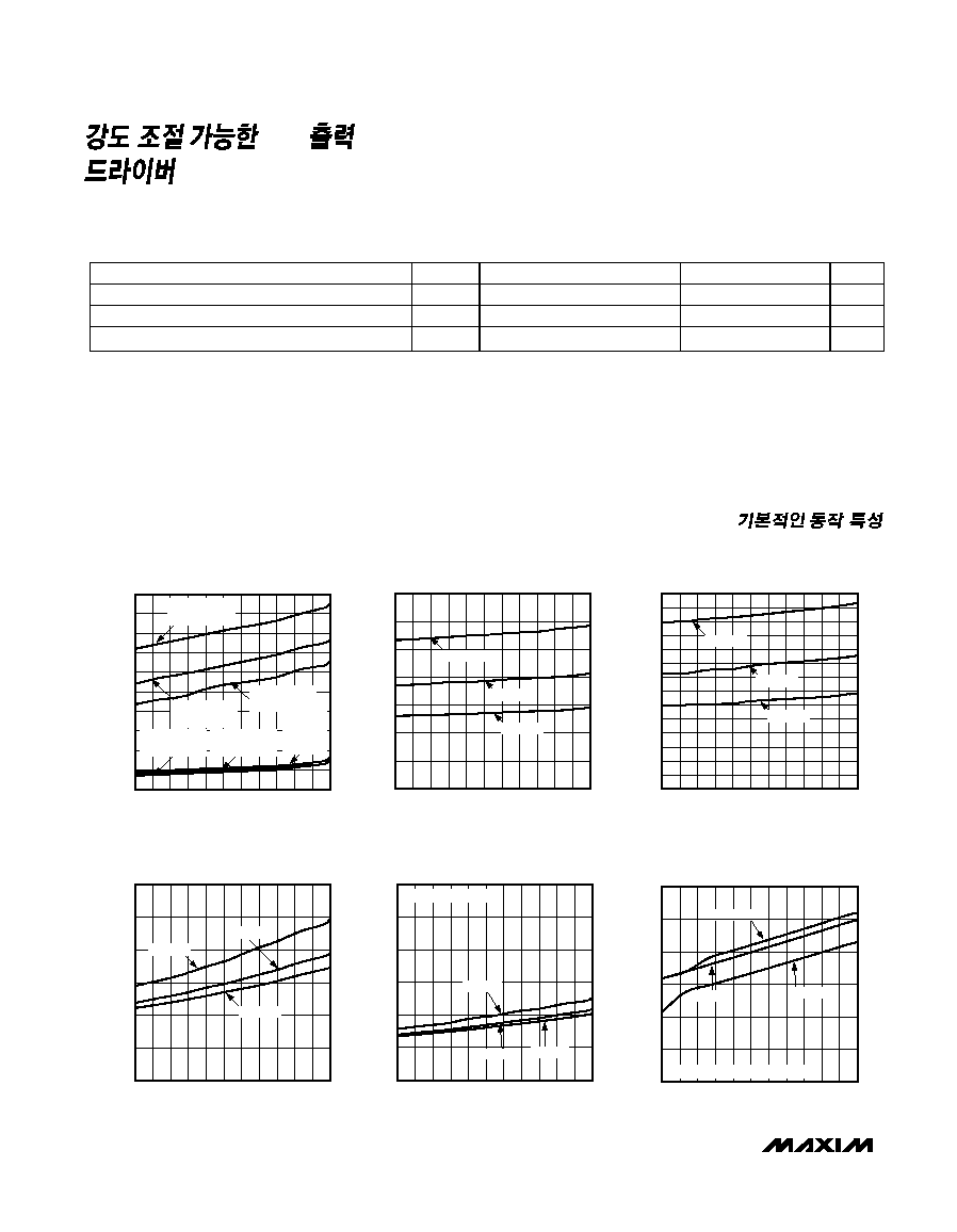
PORT OUTPUT LOW VOLTAGE WITH 50mA
LOAD CURRENT vs. TEMPERATURE
PORT OUTPUT LOW VOLTAGE V
OL
(V)
0.1
0.2
0.3
0.4
0.5
0.6
0
MAX6964 toc04
TEMPERATURE (
∞C)
110
95
65 80
-10 5
20 35 50
-25
-40
125
V+ = 3.6V
V+ = 2.7V
V+ = 2V
PORT OUTPUT LOW VOLTAGE WITH 20mA
LOAD CURRENT vs. TEMPERATURE
MAX6964 toc05
TEMPERATURE (
∞C)
PORT OUTPUT LOW VOLTAGE V
OL
(V)
110
95
80
65
50
35
20
5
-10
-25
0.1
0.2
0.3
0.4
0.5
0.6
0
-40
125
ALL OUTPUTS LOADED
V+ = 3.6V
V+ = 2.7V
V+ = 2V
PWM CLOCK FREQUENCY
vs. TEMPERATURE
MAX6964 toc06
TEMPERATURE (
∞C)
PWM CLOCK FREQUENCY (kHz)
110
95
80
65
50
35
20
5
-10
-25
-40
125
V+ = 3.6V
V+ = 2.7V
V+ = 2V
0.925
0.950
0.975
1.000
1.025
1.050
0.900
NORMALIZED TO V+ = 3.3V, T
A
= 25
∞C
STANDBY CURRENT vs. TEMPERATURE
MAX6964 toc01
TEMPERATURE (
∞C)
STANDBY CURRENT (
µ
A)
110
95
65 80
-10 5
20 35 50
-25
1
2
3
4
5
6
7
8
9
10
0
-40
125
V+ = 3.6V
PWM ENABLED
V+ = 2.7V
PWM ENABLED
V+ = 2V
PWM DISABLED
V+ = 2.7V
PWM DISABLED
V+ = 3.6V
PWM
DISABLED
V+ = 2V
PWM ENABLED
SUPPLY CURRENT vs. TEMPERATURE
(PWM DISABLED; f
SCL
= 400kHz)
MAX6964 toc02
TEMPERATURE (
∞C)
SUPPLY CURRENT (
µ
A)
110
95
65 80
-10 5
20 35 50
-25
10
20
30
40
50
60
70
0
-40
125
V+ = 3.6V
V+ = 2.7V
V+ = 2V
5
10
15
20
25
30
35
40
45
50
55
60
65
70
0
SUPPLY CURRENT vs. TEMPERATURE
(PWM ENABLED; f
SCL
= 400kHz)
MAX6964 toc03
TEMPERATURE (
∞C)
SUPPLY CURRENT (
µ
A)
110
95
65 80
-10 5
20 35 50
-25
-40
125
V+ = 3.6V
V+ = 2.7V
V+ = 2V
___________________________________________________________________
(T
A
= +25∞C, unless otherwise noted.)
TIMING CHARACTERISTICS (continued)
(Typical Operating Circuit, V+ = 2V to 3.6V, T
A
= T
MIN
to T
MAX
, unless otherwise noted. Typical values are at V+ = 3.3V, T
A
= +25∞C.)
(Note 1)
PARAMETER
SYMBOL
CONDITIONS
MIN
TYP
MAX
UNITS
Capacitive Load for Each Bus Line
C
b
(Note 3)
400
pF
RST Pulse Width
t
W
1
ns
Output Data Valid
t
DV
Figure 10
5
ns
Note 1: All parameters tested at T
A
= +25∞C. Specifications over temperature are guaranteed by design.
Note 2: A master device must provide a hold time of at least 300ns for the SDA signal (referred to V
IL
of the SCL signal) to bridge
the undefined region of SCL's falling edge.
Note 3: Guaranteed by design.
Note 4: C
b
= total capacitance of one bus line in pF. t
R
and t
F
measured between 0.3 x V
DD
and 0.7 x V
DD
.
Note 5: I
SINK
6mA. C
b
= total capacitance of one bus line in pF. t
R
and t
F
measured between 0.3 x V
DD
and 0.7 x V
DD
.
Note 6: Input filters on the SDA and SCL inputs suppress noise spikes less than 50ns.

MAX6964
17-
LED
/GPO
_______________________________________________________________________________________
5
SCOPE SHOT OF OUTPUT PORTS
MAX6964 toc07
2ms/div
OUTPUT 1,
2V/div
OUTPUT 2,
2V/div
OUTPUT 1 INDIVIDUAL INTENSITY
SET TO 1/16
MASTER INTENSITY SET TO 14/15
OUTPUT 2 INDIVIDUAL INTENSITY
SET TO 14/15
SCOPE SHOT OF OUTPUT PORTS
MAX6964 toc08
2ms/div
OUTPUT 1
2V/div
OUTPUT 2
2V/div
MASTER INTENSITY SET TO 1/15
OUTPUT 1 INDIVIDUAL INTENSITY
SET TO 1/16
OUTPUT 2 INDIVIDUAL INTENSITY
SET TO 15/16
SINK CURRENT vs. V
OL
MAX6964 toc09
SINK CURRENT (mA)
V
OL
(V)
40
30
20
10
0.05
0.10
0.15
0.20
0.25
0.30
0.35
0
0
50
V+ = 3.6V
V+ = 3.3V
V+ = 2V
V+ = 2.7V
ONLY ONE OUTPUT LOADED
______________________________________________________________
(
)
(T
A
= +25∞C, unless otherwise noted.)
QSOP
QFN
1, 4≠11, 13≠20
1≠8, 10≠17, 22
O0-O16
2
24
RST
3
23
AD0
12
9
GND
21
18
BLINK
22
19
SCL
23
20
SDA
24
21
V+
--
Pad
Exposed Pad
_____________________________________________________________________________
. 7V, 50mA
.
.
2-
.
.
. GND, V+, SCL, SDA
4
.
1
.
. GND
350mA
.
.
.
I
2
C
I
2
C
I/O
. 0.047µF
V+
GND
.
. GND
.