 | –≠–ª–µ–∫—Ç—Ä–æ–Ω–Ω—ã–π –∫–æ–º–ø–æ–Ω–µ–Ω—Ç: AN654 | –°–∫–∞—á–∞—Ç—å:  PDF PDF  ZIP ZIP |

www.maxim-ic.com/an654
Page 1 of 8
INTERFACE CIRCUITS
Application Note 654: Mar 31, 2000
New RS-232 ICs Feature 1µA Supply Current, ±15kV
ESD Protection, and 3V Operation
Application note briefly describing important features of Maxim's RS-232 transceivers with special
characteristics. Several families are described with separate and/or overlapping features: 5V only
operation through use of internal charge pumps, 3V only operation using high-efficiency internal charge
pumps, automatic shutdown to 1µA supply current when not in use and automatic wakeup when signals
are received, ±15kV ESD protection, high-efficiency driver for 50% power savings, and/or controllable
DTE or DCE function without special null-modem cable. IEC 801-2 test methods are treated, and a list of
ESD-testing DO's and DON'Ts is provided.
Maxim pioneered the use of charge-pump DC/DC converters for RS-232 interface ICs, and now offers
more than 54 such products. Maxim's first products operated from +5V, and produced outputs greater than
±5V as required by the RS-232 standard. New products feature improvements such as 3V operation (using
only four 0.1µF external capacitors), ±15kV ESD protection, and 1µA no-load supply current.
Many digital systems have moved towards 3V operation in order to increase density while decreasing
power consumption. Maxim has responded with RS-232 interface ICs that operate at 3.0V and 3.3V, many
of which use only four 0.1µF capacitors (Table 1).
Table 1. 3V and 3.3V RS-232 ICs
Maxim is the only RS-232 IC manufacturer to specify and achieve ±15kV ESD protection using both the
human body model and the IEC 801-2 air-gap discharge method (see sidebar). Maxim's extended ESD
protection eliminates the need for costly external protection devices such as TransZorbsTM, while
preventing expensive field failures.
To further simplify RS-232 applications, Maxim has recently introduced transceivers that shut down
automatically when not in use, reducing supply current to 1µA-a thousand-fold improvement over other
parts. This action helps extend battery life in portable equipment such as notebook computers, palmtop
computers, and bar-code scanners.

www.maxim-ic.com/an654
Page 2 of 8
Also simplifying applications is an internal, digitally controlled switch that transforms a Maxim RS-232
transceiver from a DTE port (Data Terminal Equipment) to a DCE port (Data Communications
Equipment).
The Move to 3V Operation
The standard supply voltage for notebook computers and other portable equipment is rapidly changing to
3V. To meet the needs of this market, many 5V RS-232 devices have been recharacterized for 3V
operation. While these parts do not generate the ±5V output swings required by RS-232 communications,
they do meet the EIA/TIA-562 requirements of ±3.7V output swings. EIA/TIA-562 is interoperable with
RS-232, although its output voltage is not sufficient to power a mouse, whose microcontroller typically
requires 5mA at 5V.
To overcome the limitations of these recharacterized devices, Maxim has developed the MAX3241 family
of 3V transceivers, which feature a low quiescent current, the capability to drive a mouse, a low-power
standby mode in which some (or all) receivers are active, a flow-through pinout, and operation to 230kbaud
(to support high-speed modems).
Unique Output Stage Uses 50% Less Power
Maxim's key innovation in developing 3V parts is a driver output structure with very low voltage drop from
input to output. Low voltage drop is important because the ideal DC/DC converter for 3.3V RS-232
transceivers is a capacitive voltage doubler. A perfect doubler would produce 6V for 3V minimum inputs,
leaving a drop of just 1V for losses in the driver output stage and the DC/DC converter itself.
Moreover, the output swing for an ideal RS-232 transceiver would be ±5V with a tolerance of zero. A
minimum of ±5V is needed to comply with the RS-232 specification, but any swing above 5V or below -
5V simply wastes power. Regardless of input voltage, therefore, members of the MAX3241 family regulate
their internal, voltage-doubling DC/DC converter to 5.4V-just enough to provide a safety margin after
covering the 200mV drop in the driver output stage. The result is minimal power consumption at the
nominal 3.3V supply rail.
An ideal (lossless) capacitive voltage doubler, unregulated, produces 6.6V with a 3.3V input and 10V with
a 5V input. Thus, an RS-232 transceiver with internal 5V doubler wastes the 5V difference between its
output (10V) and the desired ±5V as specified by the RS-232 standard. An internal 3.3V doubler, which
wastes only 1.6V, is therefore much more efficient.
Similarly, an ideal 3.3V capacitive tripler generates 9.9V. The desired output is 5V, so the overall
efficiency is only 5/9.9 (51%). Another way to compare the 3.3V doubler with the 3.3V tripler is to note
that, for every 1mA drawn by the RS-232 load, the doubler draws 2mA (from the 3.3V supply) while the
tripler must draw 3mA. Thus, the power saved by a 3.3V doubler is even greater when driving the
capacitive load of a long RS-232 cable at high speed (Figure 1).

www.maxim-ic.com/an654
Page 3 of 8
Figure 1. The MAX3241 (with voltage doubler) consumes only half as much as power as does the
competitive device based on a voltage tripler. Note also, the MAX3241 maintains valid RS-232
output levels at quadruple the data rate.
RS-232 drivers must also supply output current for driving the input resistance (3k to 7k ) associated
with the RS-232 receiver at the far end of the line, and for charging and discharging the load capacitance
(up to 2.5nF, as specified by the RS-232 standard). This charge/discharge current increases with frequency,
and exceeds the resistive current at a data rate of 80k bits/sec (40kHz). Thus, a voltage doubler at high data
rates saves even more power.
Auto-Shutdown--The Ideal RS-232 IC
The RS-232 port in most portable systems transmits and receives for only a small percentage of the time
that power is applied; for the rest of the time it may waste power needlessly. An ideal RS-232 transceiver,
therefore, should shut itself down when not transmitting or receiving.
Early RS-232 ICs for portable systems provided a shutdown pin, but the result was complete shutdown
(deep sleep) in which the chip had no way to detect incoming data. So, the next step was to provide
receivers that remained active during shutdown.
The operating system can theoretically shut down an RS-232 port if, after a suitable delay, it sees no
incoming data transitions or status-line changes. But the choice of delay period presents a problem-you can
miss data if you happen to power down just as a data burst begins, and you'll probably miss some of the
data that wakes up the system and initiates power-up. For these reasons, designers seldom go to the trouble
of introducing a monitoring delay by rewriting the BIOS/operating system.
Maxim engineers had the following goals in designing a new RS-232 transceiver:
1) Use power only when transmitting and receiving data.
2) Meet goal #1 with no compromise in performance.
3) Meet goal #1 with no increase in cost.
An obvious approach is to include a timer that shuts down the IC after a desired time interval. But this
thwarts goal #3 by increasing the die area. The better solution is to monitor all incoming data lines for valid
levels of RS-232 signal voltage. All receiver inputs will be near ground, for example, if the RS-232 port is
not connected or if the far-end transceiver is turned off. Either way, the absence of valid signal levels
causes the chip to enter its shutdown mode automatically, reducing the typical no-load supply current to
1µA.
Maxim has recently introduced four devices with automatic shutdown (Table 2). Most include an output
(valid RS-232) that indicates to the system processor whether an active RS-232 port is connected at the
other end of the cable. The MAX3212 goes one step further; it includes a transition-detect circuit whose

www.maxim-ic.com/an654
Page 4 of 8
latched output, applied as an interrupt, can wake up the system when a change of state occurs on any
incoming line.
Table 2. RS-232 Transceivers with Automatic-Shutdown Circuitry
To see the benefits of automatic shutdown, compare the supply currents of Maxim's earlier RS-232
transceivers against those of their auto-shutdown counterparts:
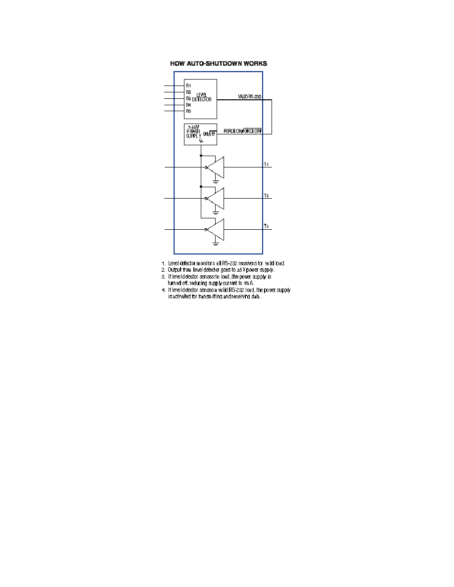
Auto-shutdown devices have Force on/force off controls (Figure 2) that can override the automatic circuitry
and force the transceiver into its low-power-standby state or its normal-operating state. When neither
control is asserted, the IC selects between these states automatically. As a result, the system saves power
without changes to the existing BIOS/operating system.
www.maxim-ic.com/an654
Page 5 of 8
Figure 2. The MAX3223 transceiver family combines ease of use (automatic shutdown) with the
+flexibility of override controls that force the IC into shutdown or normal operation.
DTE/DCE in One IC Eliminates Null Modem
Also useful for RS-232 transceivers is the capability for switching between two standard configurations:
DTE port and DCE port. The most common example is a dumb terminal or personal computer (DTE port)
connected to an external modem (DCE port). For this case, the connecting cable provides straight-through,
1-to-1 connections. Similarly, the serial cable for a printer is designed to plug into a DTE port at the
computer end.
But, problems arise if you must connect two computers together. Both are DTEs, so the standard DTE-to-
DCE cable won't work. The usual solution is a special LapLinkTM cable, or a "null modem" that converts
one of the DTE ports to a DCE. A null modem is nothing more than two back-to-back connectors with
various wires transposed. The most common type of null modem is fully implemented by a single chip
(MAX214) whose internal circuitry (under the control of a single logic-level input) performs all the
necessary wiring transpositions.
Maxim Achieves Industry's Highest ESD Protection: ±15kV
Protection level complies with human body model and IEC 801-2 air-gap discharge method
ESD (electrostatic discharge) threatens an electronic system every time someone replaces a cable or
touches an I/O port. The discharges accompanying these routine events can render an I/O port useless by
destroying one or more interface ICs connected to the port. These failures can be expensive in terms of both
warranty repairs and perceived quality.

www.maxim-ic.com/an654
Page 6 of 8
ESD can cause further damage to manufacturers, since equipment manufacturers may soon be barred from
selling to the European Community if their equipment fails to meet minimum levels of ESD performance,
as spelled out by IEC 801-2.
These two factors have led Maxim to develop a family of RS-232 products with ±15kV of ESD protection
(Table A). These interface ICs are the only ones to specify and achieve ±15kV ESD protection using both
the human body model and the IEC 801-2 air-gap discharge method. Maxim's high-ESD protection
eliminates the need for costly external protection devices such as TransZorbsTM, while preventing
expensive field failures.
Table A. RS-232-interface ICs with ±15kV ESD Protection
Older ESD Test Methods
Two methods have been commonly used for testing the ESD susceptibility of integrated circuits. The
oldest, method 3015.7 of MIL-standard 883 (also known as the human body model), was developed to aid
manufacturers in understanding the precautions necessary for packaging and handling ICs. This method
tests each package pin against all other pins, and classifies a device according to the voltage at which the
first failure occurs (which is usually on the pin most susceptible to ESD). The applied ESD waveform is
derived from a circuit called the human body model (Figure A). The capacitance (100pF) models that of the
human body, and the resistance (1500 ) models the typical series resistance in the discharge path that
includes the body, the IC, and ground.
Figure A. Most ESD standards specify the same test circuit, but with different component values.
The other method, EIAJ Method IC-121 (also known as the machine model) applies a waveform similar to
that produced when an IC makes contact with automatic handling equipment. This method was developed
by the Electronic Industries Association of Japan (EIAJ), and also uses the setup of Figure A, but with
different values for R1 and C1. The resistance represents a human holding a metallic object such as a
screwdriver, and the capacitance is that of a human body. For the resulting waveform, rise and fall times
are steeper than those for the human body model.
The two methods are complementary, so one shouldn't be chosen over the other. Because ESD can affect
ICs during manufacturing, during pc-board assembly, and after the end product is put into service, a test
should be based on both methods to provide adequate assurance of the IC's tolerance for the rigors of
manufacturing and insertion.

www.maxim-ic.com/an654
Page 7 of 8
But, neither method can accurately assess the reliability of an IC connected to the outside world. Both
methods rate an IC according to the lowest-voltage failure on any pin, which is not an adequate test if the
device includes I/O pins. I/O pins usually require (and often have) higher levels of ESD protection than do
other pins.
As an example, an IC's I/O pins might withstand ±15kV while its other pins withstand only ±2kV. The two
methods above would therefore rate the IC for only ±2kV. To resolve this problem, manufacturers are
using a newer test method-IEC 801-2 (a test developed by the European community)-for rating RS-232 ICs
and other devices that connect directly to the "outside world." As a result, the successful completion of IEC
801-2 may soon become a necessary condition for selling equipment in Europe.
Newer ESD Test Method
Although originally intended as an equipment-level test for Europe, IEC 801-2 is now gaining acceptance
worldwide as the most appropriate ESD test for IC pins accessible to users of end equipment. The IEC 801-
2 method, unlike the two previous ones, tests only I/O pins. A device's ESD rating with this method,
therefore, is determined solely by the protection afforded by its I/O pins.
IEC 801-2 specifies ESD testing by either contact discharge or air-gap discharge. The commission prefers
contact discharge, though this represents a compromise. An ESD event caused by actual contact is more
repeatable, but less realistic. Air-gap discharge is more realistic, but varies widely in amplitude according
to temperature, humidity, barometric pressure, distance, and rate of closure with the IC.
IEC 801-2 defines four levels of compliance (Table B), according to the lowest-maximum voltage
withstood by the I/O pins. The levels accommodate both contact and air-gap discharge. Maxim's ICs meet
the highest level (level four) for contact and air-gap discharge, and are the only RS-232 ICs to achieve this
level of protection.
Table B. IEC 801-2 Compliance Levels
Testing ICs for ESD ruggedness requires the use of an "ESD gun." The gun allows testing with either
contact or air-gap discharge. Contact discharge requires physical contact between the gun and the IC before
the test voltage is applied. Air-gap discharge, on the other hand, requires the gun to be charged with the test
voltage before approaching the IC (from the perpendicular, and as fast as possible). The second technique
produces a spark at some critical distance from the test unit.
ESD produced by air-gap discharge resembles actual ESD events. But, like actual ESD, the air-gap
discharge variety is not readily duplicated. It depends on many variables that are not easily controlled. IEC
801-2 therefore recommends the contact-discharge technique, attesting to the general importance of
repeatability in testing. In either case, the test procedure calls for at least ten discharges at each test level.

www.maxim-ic.com/an654
Page 8 of 8
DO's and DON'Ts of ESD Testing
1)DO USE STANDARD TEST EQUIPMENT. Repeatability in ESD testing is difficult enough as it is,
without introducing additional unknowns through home-built setups. For IEC 801-2 testing, Maxim uses an
NSG 435 ESD gun by Schaffner. For testing to MIL-STD-883 Method 3015.7, Maxim uses a Model 4000
tester by IMCS.
2) DO PERFORM A COMPLETE SET OF PARAMETRIC TESTS ON THE DEVICE UNDER TEST,
BEFORE AND AFTER THE ESD TESTING. ESD usually causes catastrophic failures, but it can also
introduce subtle and latent damage that appears later as a field failure. Leakage currents in particular should
be closely monitored to detect this damage.
3) DO TEST THE ENTIRE RANGE OF ESD VOLTAGES (not just the upper limit). Many ESD-
protection structures can withstand the highest ESD voltage for which they are guaranteed, but fail at a
lower level. Maxim tests each device pin, starting at 200V and progressing in 200V increments until failure
occurs or the ESD tester's limit is reached.
4) DO REQUIRE PERFORMANCE TO ALL RELEVANT STANDARDS. MIL-STD-883, for example,
simulates the ESD encountered by an IC during assembly and distribution (shipping). IEC 801-2, which
applies only to pins that connect outside the local system, simulates ESD events that might occur in the end
equipment.
5) DO PERFORM IEC 801-2 TESTING WITH POWER ON AS WELL AS OFF. Some competing ICs,
both bipolar and CMOS, exhibit SCR latchup when subjected to an ESD event while the power is on. SCR
latchup can cause destructive supply currents. Even if not destructive, latchup usually prevents normal
operation until removed by turning off the IC's power.
1) DON'T MISAPPLY THE STANDARDS. Some standards address the survival of all pins during
distribution and manufacturing; others address only the survival of pins that are externally accessible in the
end equipment.
2) DON'T TRUST UNSUBSTANTIATED CLAIMS that give no information regarding the test equipment
or procedures used.
3) DON'T ASSUME that bipolar ICs are inherently better than CMOS ICs, or vice-versa. What counts is
the actual performance in an application.
TMTransZorb is a trademark of General Semiconductor Industries, Inc.
TMLaplink is a trademark of Traveling Software.
MORE INFORMATION
MAX202E:
QuickView
--
Full (PDF) Data Sheet (368k)
--
Free Sample
MAX211E:
QuickView
--
Full (PDF) Data Sheet (368k)
--
Free Sample
MAX213E:
QuickView
--
Full (PDF) Data Sheet (368k)
--
Free Sample
MAX218:
QuickView
--
Full (PDF) Data Sheet (93k)
--
Free Sample
MAX232E:
QuickView
--
Full (PDF) Data Sheet (368k)
--
Free Sample
MAX241E:
QuickView
--
Full (PDF) Data Sheet (368k)
--
Free Sample
MAX3212:
QuickView
--
Full (PDF) Data Sheet (136k)
--
Free Sample
MAX3218:
QuickView
--
Full (PDF) Data Sheet (136k)
--
Free Sample
MAX3222:
QuickView
--
Full (PDF) Data Sheet (280k)
--
Free Sample
MAX3223:
QuickView
--
Full (PDF) Data Sheet (424k)
--
Free Sample
MAX3232:
QuickView
--
Full (PDF) Data Sheet (280k)
--
Free Sample
MAX3241:
QuickView
--
Full (PDF) Data Sheet (280k)
--
Free Sample
MAX3243:
QuickView
--
Full (PDF) Data Sheet (424k)
--
Free Sample
MAX560:
QuickView
--
Full (PDF) Data Sheet (352k)
--
Free Sample
MAX561:
QuickView
--
Full (PDF) Data Sheet (352k)
--
Free Sample