
SCOPE: QUAD SPST CMOS ANALOG SWITCHES
Device Type Generic Number SMD Number
01
DG201AA(x)/883B 7705301
02
HI(x)-201A/883B 7705302
Case Outline(s). The case outlines shall be designated in Mil-Std-1835 and as follows:
Outline Letter Mil-Std-1835 Case Outline Package Code
SMD (x for 01) (x for 02)
X L CDFP4-F16 16 LEAD FLATPACK F16
E K 1 GDIP1-T16 or CDIP2-T16 16 LEAD CERDIP J16
2 Z 4 CQCC1-N20 20-Pin Ceramic LCC L20
Absolute Maximum Ratings
Supply Voltage (Between V
+
and V
-
) for 01 ..................................................................... 44V
Supply Voltage (Between V
+
and V
-
) for 02 ..................................................................... 40V
Digital Input Voltage (V
IN
) for 01 1/ ........................................................... V
-
-0.3V dc to V
+
Digital Input Voltage (V
IN
) for 02 1/........................................................ V
-
-4V dc to V
+
+4V
Analog Input Voltage (V
S
) ...................................................................... V
-
-2V dc to V
+
+2V
Current, Any terminal except S or D for 01..................................................................... 30mA
Current, Any terminal except S or D for 02 .................................................................... 25mA
Continuous Current, S or D for 01 ................................................................................... 20mA
Continuous Current, S or D for 02 ................................................................................... 25mA
Peak Current S or D(Pulsed at 1ms, 10% duty cycle max) for 01.................................... 70mA
Peak Current S or D(Pulsed at 1ms, 10% duty cycle max) for 02.................................... 40mA
Lead Temperature (soldering, 10 seconds) ........................................................................ +300
∞
C
Storage Temperature ........................................................................................... -65
∞
C to +150
∞
C
Continuous Power Dissipation ............................................................................ T
A
=
+
70
∞
C
16 lead Flatpack (derate 6.1mW/
∞
C above +70
∞
C) ................................................. 485mW
16 lead CERDIP(derate 10mW/
∞
C above +70
∞
C) ................................................... 800mW
20-Pin LCC (derate 9.1mW/
∞
C above +70
∞
C) ........................................................ 727mW
Junction Temperature T
J
...................................................................................... +150
∞
C
Thermal Resistance, Junction to Case,
JC:
Case Outline 16 lead Flatpack ................................................................. 65
∞
C/W
Case Outline 16 lead CERDIP.................................................................. 50
∞
C/W
Case Outline 20-Pin LCC ........................................................................ 20
∞
C/W
Thermal Resistance, Junction to Ambient,
JA:
Case Outline 16 lead Flatpack .............................................................. 165
∞
C/W
Case Outline 16 lead CERDIP............................................................... 100
∞
C/W
Case Outline 20-Pin LCC ..................................................................... 110
∞
C/W
Recommended Operating Conditions.
Ambient Operating Range (T
A
) ................................................................ -55
∞
C to
+
125
∞
C
NOTE 1: Signals on S
X
, D
X
, or IN
X
exceeding V
+
or V
-
are clamped by internal diodes, and are
also internally current limited to 25mA.
Stresses beyond those listed under "Absolute Maximum Ratings" may cause permanent damage to the device.
These are stress ratings only, and functional operation of the device at these or any other conditions beyond
those indicated in the operational sections of the specifications is not implied. Exposure to absolute maximum
rating conditions for extended periods may affect device reliability.
----------------------------
Electrical Characteristics of DG201Axx/883B and
19-0336
Rev. B
HIx-201/883B for SMD 77053
Page 2 of
6
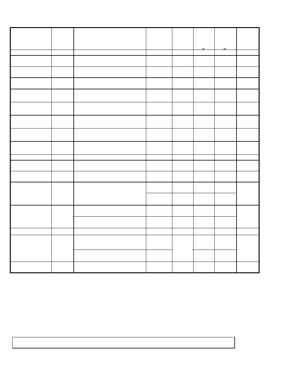
TABLE 1. ELECTRICAL TESTS
TEST
Symbol
CONDITIONS
-55
∞
C <=T
A
<= +125
∞
C
V+=+15V, V-=-15V, GND=0V
Unless otherwise specified
Group A
Subgroup
Device
type
Limits
Min
1/
Limits
Max
1/
Units
SWITCH
Analog-Signal
Range
V
ANALOG
V
S
=
±
15V
NOTE 2
1,2,3
All
-15
15
V
Drain-Source ON
Resistance
r
DS(ON)
I
D
=
±
1mA, V
D
=
±
10V, V
IN
=0.8V
1,3
2
01
175
250
Drain-Source ON
Resistance
r
DS(ON)
I
D
=
±
1mA, V
S
=
±
10V, V
IN
=0.8V
All unused channels V
A
=2.4V
1
2,3
02
70
100
Source OFF
Leakage Current
I
S(OFF)
V
S
=+/-14V,
V
D
=-/+14V, V
IN
=2.4V
1
2,3
All
-2
-100
2
100
nA
Drain OFF
Leakage Current
I
D(OFF)
V
S
=+/-14V,
V
D
=-/+14V, V
IN
=2.4V
1
2,3
01
-1
-100
1
100
nA
Drain OFF
Leakage Current
I
D(OFF)
V
S
=+/-14V,
V
D
=-/+14V, V
IN
=2.4V
1
2,3
02
-2
-100
2
100
nA
Drain ON Leakage
Current
I
D(ON)
V
D
=V
S
=
±
14V, V
IN
=0.8V
1
2,3
01
-1
-200
1
200
nA
Drain ON Leakage
Current
I
D(ON)
V
D
=V
S
=
±
14V, V
IN
=0.8V
1
2,3
02
-2
-200
2
200
nA
INPUT
Low Level Input
Voltage
V
IL
1,2,3
All
0.8 V
High Level Input
Voltage
V
IH
1,2,3
All
2.4
V
Input Leakage
Current High
I
IH
V
IN
=2.4V, 15V
1
2
1
2,3
01
02
±
1
±
10
±
0.5
±
1.0
µ
A
Input Leakage
Current Low
I
IL
V
IN
= 0V
V
IN
=0.8V
1
2
1
2,3
01
02
±
1
±
10
±
0.5
±
1.0
µ
A
SUPPLY
Positive Supply
Current
I+
V
IN
=0V
V
IN
=5V
1,2
3
1,2
3
01
4
6.5
3
4.5
mA
Negative Supply
Current
I-
V
IN
=0.8V or 2.4V
1,2
3
02
1.5
2.0
mA
----------------------------
Electrical Characteristics of DG201Axx/883B and
19-0336
Rev. B
HIx-201/883B for SMD 77053
Page 3 of
6
TEST
Symbol
CONDITIONS
-55
∞
C <=T
A
<= +125
∞
C
V+=+15V, V-=-15V, GND=0V
Unless otherwise specified
Group A
Subgroup
Device
type
Limits
Min
1/
Limits
Max
1/
Units
DYNAMIC
Turn ON time
t
ON
R
L
=1k
, CL=35pF,
V
IH
=+3V,V
IL
=0V
R
L
=1k
, CL=100pF,
V
IH
=+4V,V
IL
=0V
9,10,11
9
10,11
01
02
1000
600
800
ns
Turn OFF time
t
OFF
R
L
=1k
, CL=35pF,
V
IH
=+3V,V
IL
=0V
R
L
=1k
, CL=100pF,
V
IH
=+4V,V
IL
=0V
9
10,11
9
10,11
01
02
500
650
500
650
ns
NOTE 1: The limiting terms "min" (minimum) and "max" (maximum) shall be considered to apply to magnitudes
only. Negative current shall be defined as conventional current flow out of a device terminal.
NOTE 2: Guaranteed, if not tested, to the limits specified.
FIGURE 1: SWITCHING TIME TEST CIRCUIT: See Commercial Data Sheet
TRUTH TABLE TERMINAL CONNECTION
Device Type
Logic
Switch
Terminal
NUMBER
DG201A &
HIx-201
DG201A &
HIx-201
01 & 02
0
ON
J16 & F16
L20
1
OFF
1
IN
1
NC
2
D
1
IN
1
3
S
1
D
1
4
V-
S
1
5
GND
V-
6
S
4
NC
7
D
4
GND
8
IN
4
S
4
9
IN
3
D
4
10
D
3
IN
4
11
S
3
NC
12
NC (01)
IN
3
3/ 12
V
REF
(02)
IN3
ORDERING
INFORMATION
13
V+
D
3
SMD #
Maxim #
Pkg.
14
S
2
S
3
7705301EA
DG201AAK/883B
J16
15
D
2
NC (01)
7705301XC
DG201AAL/883B
F16
3/ 15
D
2
V
REF
(02)
77053012C
DG201AAZ/883B
L20
16
IN
2
NC
7705302EA
HI1-201/883B
J16
17
V+
77053022C
HI4-201/883B
L20
18
S
2
19
D
2
20
IN
2
NOTE 3: V
REF
is normally floating, but voltage up to 10V can be applied to raise the threshold voltage.
----------------------------
Electrical Characteristics of DG201Axx/883B and
19-0336
Rev. B
HIx-201/883B for SMD 77053
Page 4 of
6

QUALITY ASSURANCE
Sampling and inspection procedures shall be in accordance with MIL-Prf-38535, Appendix A as specified in Mil-
Std-883.
Screening shall be in accordance with Method 5004 of Mil-Std-883. Burn-in test Method 1015:
1. Test Condition, A, B, C, or D.
2. TA = +125
∞
C minimum.
3. Interim and final electrical test requirements shall be specified in Table 2.
Quality conformance inspection shall be in accordance with Method 5005 of Mil-Std-883, including Groups A, B,
C, and D inspection.
Group A inspection:
1. Tests as specified in Table 2.
2. Selected subgroups in Table 1, Method 5005 of Mil-Std-883 shall be omitted.
Group C and D inspections:
a. End-point electrical parameters shall be specified in Table 1.
b. Steady-state life test, Method 1005 of Mil-Std-883:
1. Test condition A, B, C, D.
2. TA = +125
∞
C, minimum.
3. Test duration, 1000 hours, except as permitted by Method 1005 of Mil-Std-883.
TABLE 2. ELECTRICAL TEST REQUIREMENTS
Mil-Std-883 Test Requirements
Subgroups
per Method 5005, Table 1
Interim Electric Parameters
Method 5004
1
Final Electrical Parameters
Method 5005
1*, 2, 3, 9
Group A Test Requirements
Method 5005
1, 2, 3, 9, 10, 11
Group C and D End-Point Electrical Parameters
Method 5005
1
* PDA applies to Subgroup 1 only.
----------------------------
Electrical Characteristics of DG201Axx/883B and
19-0336
Rev. B
HIx-201/883B for SMD 77053
Page 5 of
6