MAX1065 DS
General Description
The MAX1065/MAX1066 14-bit, low-power successive
approximation analog-to-digital converters (ADCs) fea-
ture automatic power-down, a factory-trimmed internal
clock, and a high-speed, 14-bit-wide (MAX1065) or
byte-wide (MAX1066) parallel interface. The devices
operate from a single 4.75V to 5.25V analog supply and
a 2.7V to 5.25V digital supply.
The MAX1065/MAX1066 use an internal 4.096V refer-
ence or an external reference. The MAX1065/MAX1066
consume only 1.8mA at a sampling rate of 165ksps with
external reference and 2.7mA with internal reference.
AutoShutdownTM reduces supply current to 0.1mA at
10ksps.
The MAX1065/MAX1066 are ideal for high-performance,
battery-powered, data-acquisition applications.
Excellent dynamic performance and low-power con-
sumption in a small package make the MAX1065/
MAX1066 the best choice for circuits with demanding
power consumption and space requirements.
The 14-bit-wide MAX1065 is available in a 28-pin TSSOP
package, and the byte-wide MAX1066 is available in a
20-pin TSSOP package. Both devices are available in
either the 0°C to +70°C commercial, or the -40°C to
+85°C extended temperature range.
Applications
Features
o 14-Bit-Wide (MAX1065) and Byte-Wide (MAX1066)
Parallel Interface
o High Speed: 165ksps Sample Rate
o Accurate: ±1LSB DNL (max), ±1LSB INL (max)
o 4.096V, 35ppm/°C Internal Reference
o External Reference Range 3.8V to 5.25V
o Single 4.75V to 5.25V Analog Supply Voltage
o 2.7V to 5.25V Digital Supply Voltage
o Low Supply Current
1.8mA (External Reference)
2.7mA (Internal Reference)
0.1mA AutoShutdown Mode (10ksps, External
Reference)
o Small Footprint
28-Pin TSSOP Package (14-Bit Wide)
20-Pin TSSOP Package (Byte Wide)
MAX1065/MAX1066
Low-Power, 14-Bit Analog-to-Digital Converters
with Parallel Interface
________________________________________________________________ Maxim Integrated Products
1
Ordering Information
ANALOG INPUT
D0D13
EOC
REFADJ
REF
DGND
AGND
RESET
CS
R/C
AIN
AV
DD
DV
DD
MAX1065
0.1
µF
0.1
µF
5V ANALOG
5V DIGITAL
0.1
µF
1
µF
µP DATA
BUS
Typical Operating Circuit
19-2466; Rev 0; 4/02
For pricing, delivery, and ordering information, please contact Maxim/Dallas Direct! at
1-888-629-4642, or visit Maxim's website at www.maxim-ic.com.
Pin Configurations appear at end of data sheet.
AutoShutdown is a registered trademark of Maxim Integrated
Products, Inc.
PART
TEMP RANGE
PIN-
PACKAGE
INL
MAX1065ACUI
0°C to 70°C
28 TSSOP
±1
MAX1065BCUI
0°C to 70°C
28 TSSOP
±2
MAX1065CCUI
0°C to 70°C
28 TSSOP
±3
MAX1065AEUI
-40°C to +85°C
28 TSSOP
±1
MAX1065BEUI
-40°C to +85°C
28 TSSOP
±2
MAX1065CEUI
-40°C to +85°C
28 TSSOP
±3
MAX1066ACUP
0°C to 70°C
20 TSSOP
±1
MAX1066BCUP
0°C to 70°C
20 TSSOP
±2
MAX1066CCUP
0°C to 70°C
20 TSSOP
±3
MAX1066AEUP
-40°C to +85°C
20 TSSOP
±1
MAX1066BEUP
-40°C to +85°C
20 TSSOP
±2
MAX1066CEUP
-40°C to +85°C
20 TSSOP
±3
Temperature
Sensor/Monitor
Industrial Process
Control
I/O Boards
Data-Acquisition
Systems
Cable/Harness Tester
Accelerometer
Measurements
Digital Signal Processing
MAX1065/MAX1066
Low-Power, 14-Bit Analog-to-Digital Converters
with Parallel Interface
2
_______________________________________________________________________________________
ABSOLUTE MAXIMUM RATINGS
ELECTRICAL CHARACTERISTICS
(AV
DD
= DV
DD
= 5V, external reference = 4.096V, C
REF
= 1µF, C
REFADJ
= 0.1µF, T
A
= T
MIN
to T
MAX
, unless otherwise noted.
Typical values are at T
A
= +25°C.)
Stresses beyond those listed under "Absolute Maximum Ratings" may cause permanent damage to the device. These are stress ratings only, and functional
operation of the device at these or any other conditions beyond those indicated in the operational sections of the specifications is not implied. Exposure to
absolute maximum rating conditions for extended periods may affect device reliability.
AV
DD
to AGND .........................................................-0.3V to +6V
DV
DD
to DGND.........................................................-0.3V to +6V
AGND to DGND.....................................................-0.3V to +0.3V
AIN, REF, REFADJ to AGND....................-0.3V to (AV
DD
+ 0.3V)
CS, HBEN, R/C, RESET to DGND ............................-0.3V to +6V
Digital Output (D13D0, EOC)
to DGND ..................................................-0.3V to (DV
DD
+ 0.3V)
Maximum Continuous Current Into Any Pin ........................50mA
Continuous Power Dissipation (T
A
= +70°C)
20-Pin TSSOP (derate 10.9mW/°C above +70°C) .......879mW
28-Pin TSSOP (derate 12.8mW/°C above +70°C) .....1026mW
Operating Temperature Ranges
MAX106_ _CU_ ...................................................0°C to +70°C
MAX106_ _EU_ ................................................-40°C to +85°C
Storage Temperature Range .............................-65°C to +150°C
Junction Temperature ......................................................+150°C
Lead Temperature (soldering, 10s) .................................+300°C
PARAMETER
SYMBOL
CONDITIONS
MIN
TYP
MAX
UNITS
DC ACCURACY
Resolution
N
14
Bits
MAX106_A
±1
MAX106_B
±2
Relative Accuracy (Note 1)
INL
MAX106_C
±3
LSB
Differential Nonlinearity
DNL
No missing codes over temperature
±1
LSB
Transition Noise
RMS noise, includes quantization
noise
0.32
LSB
RMS
Offset Error
0.2
1
mV
Gain Error
(Note 2)
±0.002
±0.02
%FSR
Offset Drift
0.6
ppm/°C
Gain Drift
0.2
ppm/°C
DYNAMIC PERFORMANCE (f
IN(SINE-WAVE)
= 1kHz, V
IN
= 4.096V
P-P
, 165ksps)
Signal-to-Noise Plus Distortion
SINAD
81
84
dB
Signal-to-Noise Ratio
SNR
82
84
dB
Total Harmonic Distortion
THD
-99
-86
dB
Spurious-Free Dynamic Range
SFDR
87
102
dB
Full-Power Bandwidth
-3dB point
4
MHz
Full-Linear Bandwidth
SINAD > 81dB
20
kHz
CONVERSION RATE
Sample Rate
f
SAMPLE
165
ksps
Aperture Delay
40
ns
Aperture Jitter
100
ps
ANALOG INPUT
Input Range
V
AIN
0
V
REF
V
Input Capacitance
C
AIN
40
pF
MAX1065/MAX1066
Low-Power, 14-Bit Analog-to-Digital Converters
with Parallel Interface
_______________________________________________________________________________________
3
ELECTRICAL CHARACTERISTICS (continued)
(AV
DD
= DV
DD
= 5V, external reference = 4.096V, C
REF
= 1µF, C
REFADJ
= 0.1µF, T
A
= T
MIN
to T
MAX
, unless otherwise noted.
Typical values are at T
A
= +25°C.)
PARAMETER
SYMBOL
CONDITIONS
MIN
TYP
MAX
UNITS
INTERNAL REFERENCE
REF Output Voltage
V
REF
4.056
4.096
4.136
V
REF Output Tempco
TC
REF
±35
ppm/°C
REF Short-Circuit Current
I
REFSC
±10
mA
Capacitive Bypass at REFADJ
C
REFADJ
0.1
µF
Capacitive Bypass at REF
C
REF
1
µF
REFADJ Input Leakage Current
I
REFADJ
20
µA
EXTERNAL REFERENCE
REFADJ Buffer Disable
Threshold
To power-down the internal reference
AV
DD
-
0.4
AV
DD
-
0.1
V
REF Input Voltage Range
Internal reference disabled
3.8
AV
DD
V
V
REF
= 4.096V, f
SAMPLE
= 165ksps
62
120
REF Input Current
I
REF
Shutdown mode
±0.1
µA
DIGITAL INPUTS/OUTPUTS (
CS, R/C, EOC, D0D13, RESET, HBEN)
Input High Voltage
V
IH
0.7 x
DV
DD
Input Low Voltage
V
IL
0.3 x
DV
DD
V
Input Leakage Current
I
IN
V
IH
= 0 or DV
DD
±0.1
±1
µA
Input Hysteresis
V
HYST
0.1
V
Input Capacitance
C
IN
15
pF
Output High Voltage
V
OH
I
SOURCE
= 0.5mA,
DV
DD
= 2.7V to 5.25V,
AV
DD
= 5.25V
D
VDD
-
0.4
V
Output Low Voltage
V
OL
I
SINK
= 1.6mA,
DV
DD
= 2.7V to 5.25V,
AV
DD
= 5.25V
0.4
V
Three-State Leakage Current
I
OZ
D0D13
±0.1
±10
µA
Three-State Output
Capacitance
C
OZ
15
pF
POWER REQUIREMENTS
Analog Supply Voltage
AV
DD
4.75
5.25
V
Digital Supply Voltage
DV
DD
2.7
AV
DD
V
165ksps
2.7
3.2
100ksps
2.0
10ksps
1.0
Internal reference
1ksps
1.0
165ksps
1.8
2.3
100ksps
1.1
10ksps
0.1
Analog Supply Current
I
AVDD
External reference
1ksps
0.01
mA
MAX1065/MAX1066
Low-Power, 14-Bit Analog-to-Digital Converters
with Parallel Interface
4
_______________________________________________________________________________________
ELECTRICAL CHARACTERISTICS (continued)
(AV
DD
= DV
DD
= 5V, external reference = 4.096V, C
REF
= 1µF, C
REFADJ
= 0.1µF, T
A
= T
MIN
to T
MAX
, unless otherwise noted.
Typical values are at T
A
= +25°C.)
PARAMETER
SYMBOL
CONDITIONS
MIN
TYP
MAX
UNITS
165ksps
0.5
0.7
100ksps
0.3
10ksps
0.03
Digital Supply Current
I
DVDD
D0D13 = all zeros
1ksps
0.003
mA
I
AVDD
0.05
5
mA
Full power-down
I
DVDD
0.5
5
µA
I
AVDD
1.0
1.2
mA
Shutdown Supply Current
(Note 3)
I
SHDN
REF and REF
buffer enabled
(standby mode)
I
DVDD
0.5
5
µA
Power-Supply Rejection Ratio
(Note 4)
PSRR
AV
DD
= 5V, ±5%, full-scale input
68
dB
TIMING CHARACTERISTICS (Figures 1 and 2)
(AV
DD
= 4.75V to 5.25V, DV
DD
= 2.7V to AV
DD
, external reference = 4.096V, C
REF
= 1µF, C
REFADJ
= 0.1µF, C
D13D0,
C
EOC
= 20pF,
T
A
= T
MIN
to T
MAX
, unless otherwise noted. Typical values are at T
A
= +25°C.)
PARAMETER
SYMBOL
CONDITIONS
MIN
TYP
MAX
UNITS
Acquisition Time
t
ACQ
1.1
Conversion Time
t
CONV
4.7
µs
CS Pulse Width High
t
CSH
(Note 5)
40
ns
V
DVDD
= 4.75V to 5.25V
40
CS Pulse Width Low
t
CSL
(Note 5)
V
DVDD
= 2.7V to 4.74V
60
ns
R/
C to CS Fall Setup Time
t
DS
0
ns
V
DVDD
= 4.75V to 5.25V
40
R/
C to CS Fall Hold Time
t
DH
V
DVDD
= 2.7V to 5.25V
60
ns
V
DVDD
= 4.75V to 5.25V
40
CS to Output Data Valid
t
DO
V
DVDD
= 2.7V to 4.74V
80
ns
V
DVDD
= 4.75V to 5.25V
40
HBEN Transition To
Output Data Valid
(MAX1066 only)
t
DO1
V
DVDD
= 2.7V to 4.74V
80
ns
EOC Fall To CS Fall
t
DV
0
ns
V
DVDD
= 4.75V to 5.25V
40
CS Rise To EOC Rise
t
EOC
V
DVDD
= 2.7V to 4.74V
80
ns
V
DVDD
= 4.75V to 5.25V
40
Bus Relinquish Time
(Note 5)
t
BR
V
DVDD
= 2.7V to 4.74V
80
ns
Note 1: Relative accuracy is the deviation of the analog value at any code from its theoretical value after offset and gain errors have
been removed.
Note 2: Offset nulled.
Note 3: Maximum specification is limited by automated test equipment.
Note 4: Defined as the change in positive full scale caused by a ±5% variation in the nominal supply.
Note 5: To ensure best performance, finish reading the data and wait t
BR
before starting a new acquisition.
MAX1065/MAX1066
Low-Power, 14-Bit Analog-to-Digital Converters
with Parallel Interface
_______________________________________________________________________________________
5
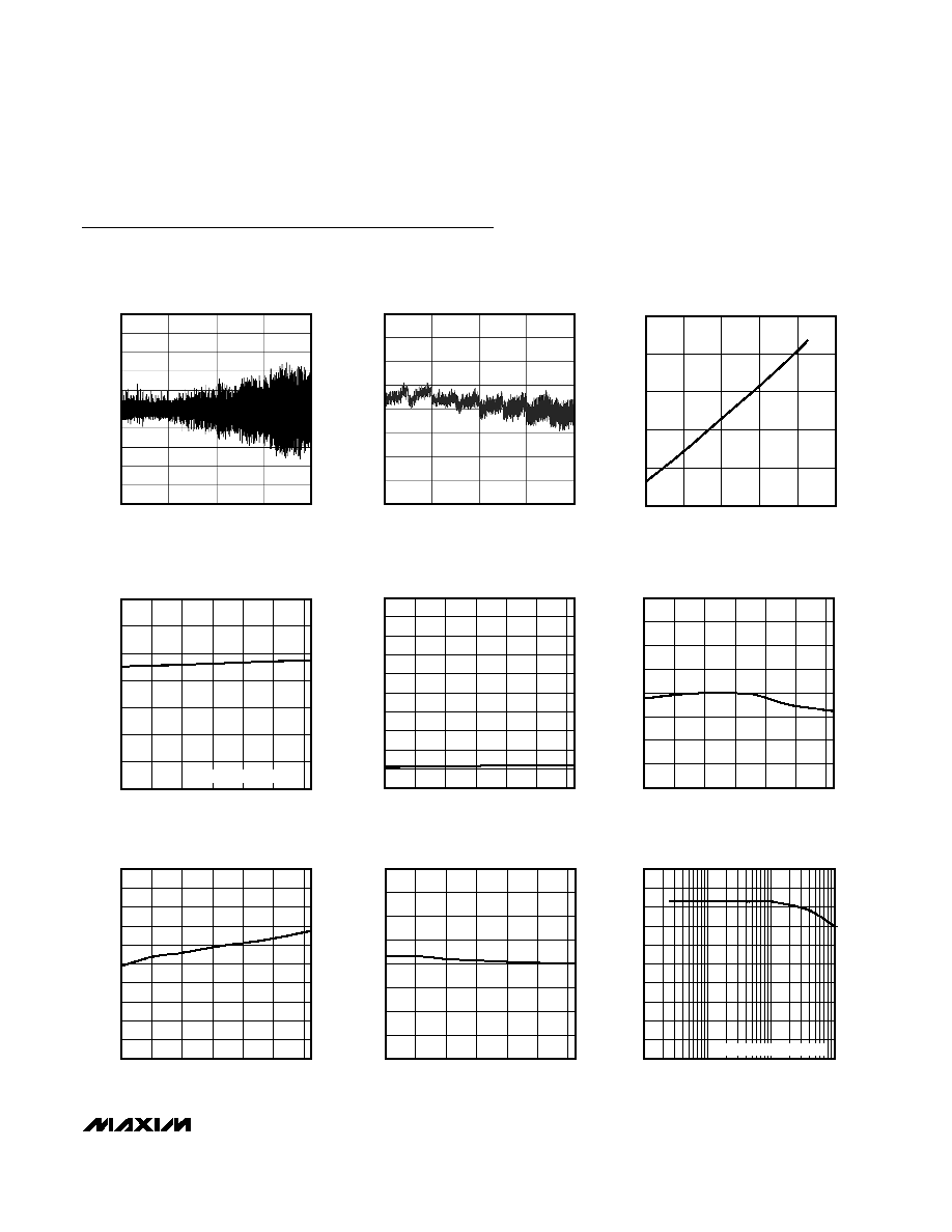
DNL vs. OUTPUT CODE
MAX1065/MAX1066 toc01
OUTPUT CODE
DNL (LSB)
12288
8192
4096
-0.8
-0.6
-0.4
-0.2
0
0.2
0.4
0.6
0.8
1.0
-1.0
0
16384
INL vs. OUTPUT CODE
MAX1065/MAX1066 toc02
OUTPUT CODE
INL (LSB)
12288
8192
4096
-1.5
-1.0
-0.5
0
0.5
1.0
1.5
2.0
-2.0
0
16384
I
AVDD
+ I
DVDD
SUPPLY CURRENT
vs. SAMPLE RATE
MAX1065/MAX1066 toc03
CONVERSION RATE (ksps)
SUPPLY CURRENT (mA)
100
10
1
0.1
0.001
0.01
0.1
1
10
0.0001
0.01
1000
I
AVDD
+ I
DVDD
SUPPLY CURRENT
vs. TEMPERATURE
MAX1065/MAX1066 toc04
TEMPERATURE (
°C)
SUPPLY CURRENT (mA)
80
60
40
20
0
-20
0.5
1.0
1.5
2.0
2.5
3.0
3.5
0
-40
SAMPLE RATE = 165ksps
I
AVDD
+ I
DVDD
SHUTDOWN CURRENT
vs. TEMPERATURE
MAX1065/MAX1066 toc05
TEMPERATURE (
°C)
SHUTDOWN CURRENT (
µ
A)
80
60
40
20
0
-20
5.0
0
-40
0.5
1.0
1.5
2.0
2.5
3.0
3.5
4.0
4.5
INTERNAL REFERENCE
vs. TEMPERATURE
MAX1065/MAX1066 toc06
TEMPERATURE (
°C)
INTERNAL REFERENCE (V)
80
60
40
20
0
-20
4.136
4.056
-40
4.066
4.076
4.086
4.096
4.106
4.116
4.126
OFFSET ERROR vs. TEMPERATURE
MAX1065/MAX1066 toc07
TEMPERATURE (
°C)
OFFSET ERROR (
µ
V)
80
60
40
20
0
-20
1000
0
-40
-800
-600
-400
-200
0
200
400
600
800
GAIN ERROR vs. TEMPERATURE
MAX1065/MAX1066 toc08
TEMPERATURE (
°C)
GAIN ERROR (%FSR)
80
60
40
20
0
-20
0.020
-0.020
-40
-0.015
-0.010
-0.005
0
0.005
0.010
0.015
SINAD vs. FREQUENCY
MAX1065/MAX1066 toc09
FREQUENCY (kHz)
SINAD (dB)
10
1
10
20
30
40
50
60
70
80
90
100
0
0.1
100
SAMPLE RATE = 165ksps
Typical Operating Characteristics
(AV
DD
= DV
DD
= 5V, external reference = 4.096V, C
REF
= 1µF, C
REFADJ
= 0.1µF, T
A
= +25°C, unless otherwise noted.)