 | –≠–ª–µ–∫—Ç—Ä–æ–Ω–Ω—ã–π –∫–æ–º–ø–æ–Ω–µ–Ω—Ç: MAX7841 | –°–∫–∞—á–∞—Ç—å:  PDF PDF  ZIP ZIP |
For pricing delivery, and ordering information please contact Maxim/Dallas Direct! at
1-888-629-4642, or visit Maxim's website at www.maxim-ic.com.
General Description
The MX7841 contains eight 14-bit, voltage-output digi-
tal-to-analog converters (DACs). On-chip precision out-
put amplifiers provide the voltage outputs. The device
operates from ±15V supplies. Its bipolar output voltage
swing ranges from (V
SS
+ 2.5V) to (V
DD
- 2.5V) and is
achieved with no external components. The MX7841
has three pairs of differential reference inputs; two of
these pairs are connected to two DACs each, and a
third pair is connected to four DACs. The references
are independently controlled, providing different full-
scale output voltages to the respective DACs.
The MX7841 features double-buffered interface logic
with a 14-bit parallel data bus. Each DAC has an input
latch and a DAC latch. Data in the DAC latch sets the
output voltage. The eight input latches are addressed
with three address lines. Data is loaded to the input
latch with a single write instruction. An asynchronous
load input (LDAC) transfers data from the input latch to
the DAC latch. The LDAC input controls all DACs;
therefore, all DACs can be updated simultaneously by
asserting LDAC.
An asynchronous CLR input sets the output of all eight
DACs to the respective DUTGND input of the op amp.
Note that CLR is a CMOS input, which is powered by
V
DD
. All other logic inputs are TTL/CMOS compatible.
The MX7841 is pin-for-pin compatible with AD7841.
Applications
Automatic Test Equipment (ATE)
Industrial Process Controls
Arbitrary Function Generators
Avionics Equipment
Minimum Component Count Analog Systems
Digital Offset/Gain Adjustment
SONET Applications
Features
o Full 14-Bit Performance Without Adjustments
o Eight DACs in a Single Package
o Buffered Voltage Outputs
o Unipolar or Bipolar Voltage Swing of (V
SS
+ 2.5V)
to (V
DD
- 2.5V)
o 31µs Output Settling Time
o Low Power Consumption: 8mA (typ)
o Small 44-Pin MQFP Package
o Double-Buffered Digital Inputs
o Asynchronous Load Updates All DACs
Simultaneously
o Asynchronous CLR Forces All DACs to
DUTGND_ _ Potential
MX7841
Octal, 14-Bit Voltage-Output DAC
with Parallel Interface
________________________________________________________________ Maxim Integrated Products
1
DUTGNDGH
OUTH
REFGH-
REFGH+
CLR
DB13
DB12
DB11
DB10
DB9
DB8
DUTGNDAB
OUTA
REFAB-
REFAB+
V
DD
V
SS
LDAC
A2
A1
A0
CS
1
2
3
4
5
6
7
8
9
10
11
12
13
14
15
16
17
18
19
20
21
22
44
43
42
41
40
39
38
37
36
35
34
33
32
31
30
29
28
27
26
25
24
23
WR
V
CC
GND
DB0
DB1
DB2
DB3
DB4
DB5
DB6
DB7
OUTB
OUTC
DUTGNDCD
OUTD
REFCDEF-
REFCDEF+
V
DD
OUTE
DUTGNDEF
OUTF
OUTG
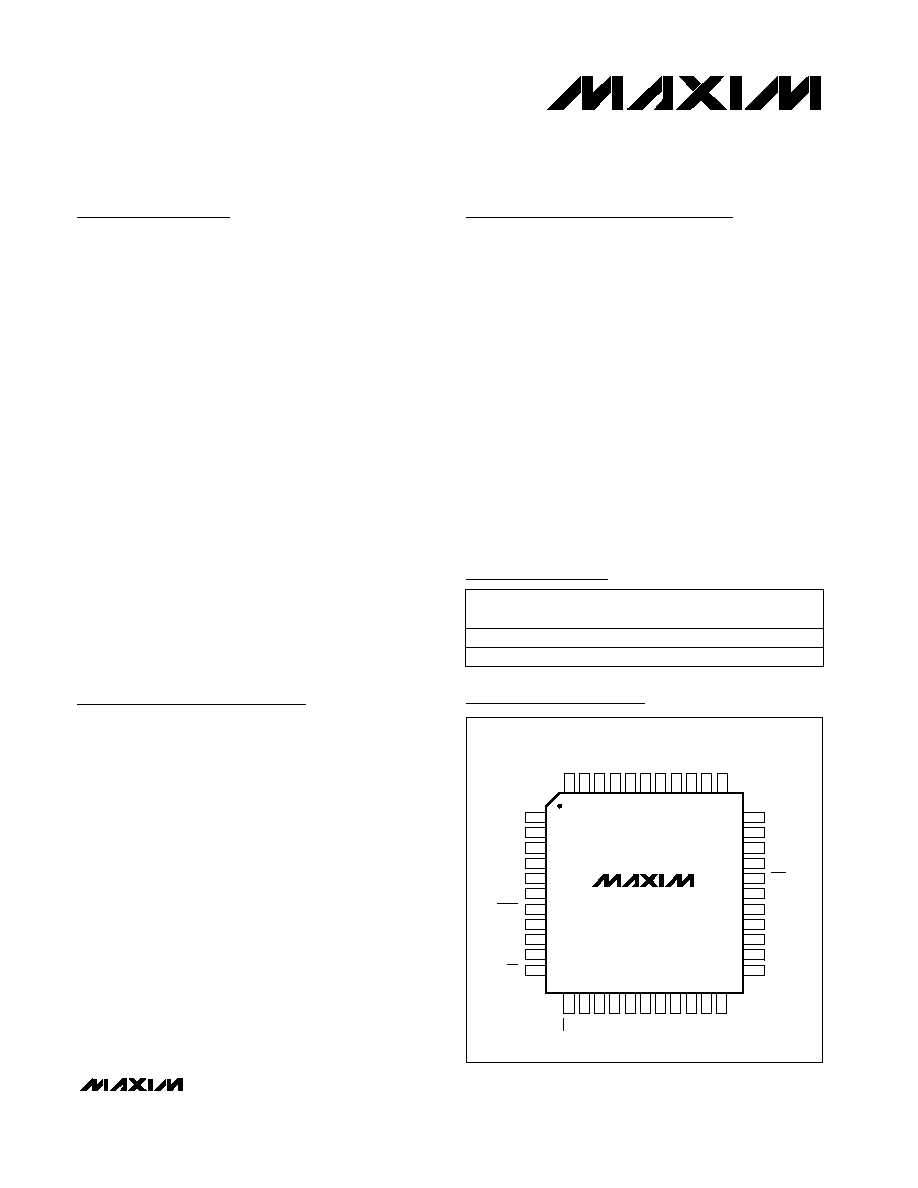
MQFP
MX7841
TOP VIEW
19-2953; Rev 0; 7/03
PART
MX7841BS
MX7841AS
-40∞C to +85∞C
-40∞C to +85∞C
TEMP RANGE
PIN-
PACKAGE
44 MQFP
44 MQFP
Functional Diagram appears at end of data sheet.
Pin Configuration
Ordering Information
INL
(LSB)
±2
±4

MX7841
Octal, 14-Bit Voltage-Output DAC
with Parallel Interface
2
_______________________________________________________________________________________
ABSOLUTE MAXIMUM RATINGS
Stresses beyond those listed under "Absolute Maximum Ratings" may cause permanent damage to the device. These are stress ratings only, and functional
operation of the device at these or any other conditions beyond those indicated in the operational sections of the specifications is not implied. Exposure to
absolute maximum rating conditions for extended periods may affect device reliability.
V
DD
to GND ...........................................................-0.3V to +17V
V
SS
to GND ........................................................... -17V to +0.3V
V
CC
to GND ............................................................ -0.3V to +6V
A_, DB_, WR, CS, LDAC, CLR to GND .....+0.3V to (V
CC
+ 0.3V)
REF_ _ _ _+, REF_ _ _ _-,
DUTGND_ _ .................................(V
SS
- 0.3V) to (V
DD
+ 0.3V)
OUT_ ..........................................................................V
DD
to V
SS
Maximum Current into REF_ _ _ _ _, DUTGND_ _ ...........±10mA
Maximum Current into Any Signal Pin ..............................±50mA
OUT_ Short-Circuit Duration to V
DD
, V
SS
, and GND ................1s
Continuous Power Dissipation (T
A
= +70∞C)
44-Pin MQFP (derate 11.1mW/∞C above +70∞C).........870mW
Operating Temperature Range ...........................-40∞C to +85∞C
Junction Temperature ......................................................+150∞C
Storage Temperature Range .............................-65∞C to +150∞C
Lead Temperature (soldering, 10s) .................................+300∞C
(Note 1)
MX7841BS
(Note 1)
(Note 1)
MX7841AS
Guaranteed monotonic
CONDITIONS
0.5
DC Output Impedance
pF
50
Capacitive Load to GND
k
5
Resistive Load to GND
V
(V
SS
+ 2.5) to
(V
DD
- 2.5)
Output Voltage Swing
V
2
10
(REF_ _ _ _+) - (REF_ _ _ _-)
Range
V
-5
0
REF_ _ _ _- Input Range
V
0
5
REF_ _ _ _+ Input Range
µA
±1
Input Current
M
100
Input Resistance
±2
Bits
14
N
Resolution
µV
75
120
DC Crosstalk
ppm
FSR/∞C
0.5
10
Gain Temperature Coefficient
LSB
±2
Gain Error
LSB
±4
INL
Relative Accuracy
LSB
±1
DNL
Differential Nonlinearity
LSB
±2
±8
Full-Scale Error
UNITS
MIN
TYP
MAX
SYMBOL
PARAMETER
ELECTRICAL CHARACTERISTICS
(V
DD
= +15V ±10%, V
SS
= -15V ±10%, V
CC
= +5V ±5%, V
GND
= V
DUTGND_ _
= 0, V
REF
_ _ _ _+ = +5V, V
REF
_ _ _ _- = -5V, R
L
= 5k
,
C
L
= 50pF, T
A
= T
MIN
to T
MAX
, unless otherwise noted. Typical values are at T
A
= +25∞C.)
LSB
±2
±8
Zero-Scale Error
STATIC PERFORMANCE (ANALOG SECTION)
REFERENCE INPUTS
ANALOG OUTPUTS
MX7841
Octal, 14-Bit Voltage-Output DAC
with Parallel Interface
_______________________________________________________________________________________
3
ELECTRICAL CHARACTERISTICS (continued)
(V
DD
= +15V ±10%, V
SS
= -15V ±10%, V
CC
= +5V ±5%, V
GND
= V
DUTGND_ _
= 0, V
REF
_ _ _ _+ = +5V, V
REF
_ _ _ _- = -5V, R
L
= 5k
,
C
L
= 50pF, T
A
= T
MIN
to T
MAX
, unless otherwise noted. Typical values are at T
A
= +25∞C.)
INTERFACE TIMING CHARACTERISTICS
(V
DD
= +15V ±10%, V
SS
= -15V ±10%, V
CC
= +5V ±5%, V
GND
= V
DUTGND_ _
= 0, V
REF
_ _ _ _+ = +5V, V
REF
_ _ _ _- = -5V, Figure 2a,
T
A
= T
MIN
to T
MAX
, unless otherwise noted.)
CONDITIONS
k
60
Input Impedance per DAC
µA
±300
Maximum Input Current per DAC
UNITS
MIN
TYP
MAX
SYMBOL
PARAMETER
Digital inputs = 0V or V
CC
µA
±1
±10
I
IN
V
-2
+2
Input Range
Input Current
V
4.75
5.25
V
CC
V
CC
Digital Power Supply
V
13.5
16.5
V
DD
V
DD
Analog Power-Supply
Range
V
-16.75
-13.5
V
SS
V
SS
Analog Power-Supply
Range
V
SS
= -15V ±5%
V
DD
= +15V ±5%
dB
90
R
L
=
dB
R
L
=
90
PSRR,
V
OUT
/
V
DD
PSRR,
V
OUT
/
V
SS
mA
8
10
I
SS
mA
8
10
I
DD
Positive Supply Current
Negative Supply Current
(Note 2)
mA
0.5
I
CC
Digital Supply Current
ns
0
t
4
ns
50
t
3
LDAC Pulse Width Low
CS Low to WR Low
CONDITIONS
ns
50
t
1
CS Pulse Width Low
ns
50
t
2
WR Pulse Width Low
UNITS
MIN
TYP
MAX
SYMBOL
PARAMETER
ns
15
t
8
ns
0
t
7
Data Valid to WR Hold
Address Valid to WR Setup
ns
0
t
5
CS High to WR High
ns
20
t
6
Data Valid to WR Setup
ns
0
t
9
Address Valid to WR Hold
(Note 1)
pF
10
C
IN
Input Capacitance
V
2.4
V
IH
Input Voltage High
V
0.8
V
IL
Input Voltage Low
DUTGND_ _ CHARACTERISTICS
POWER SUPPLIES
DIGITAL INPUTS
(Figure 2b)
ns
300
t
10
CLR Pulse-Activation Time
MX7841
Octal, 14-Bit Voltage-Output DAC
with Parallel Interface
4
_______________________________________________________________________________________
Note 1: Guaranteed by design. Not production tested.
Note 2: All digital inputs (DB_, A_, WR, CS, LDAC, and CLR) at GND or V
CC
potential.
Note 3: All digital inputs (DB_, A_, WR, CS, LDAC, and CLR) at +0.8V or +2.4V.
Note 4: All digital inputs (DB0 to DB13) transition from GND to V
CC
with WR = V
CC
DYNAMIC CHARACTERISTICS
(V
DD
= +15V ±10%, V
SS
= -15V ±10%, V
CC
= +5V ±5%, V
GND
= V
DUTGND_ _
= 0, V
REF
_ _ _ _+ = +5V, V
REF
_ _ _ _- = -5V, R
L
= 5k
,
C
L
= 50pF, T
A
= T
MIN
to T
MAX
, unless otherwise noted. Typical values are at T
A
= +25∞C.)
(Note 4)
(Note 3)
V
REF+
= V
REF-
= 0
0.2
To ±0.5 LSB of full scale
0.1
Digital Feedthrough
Digital Crosstalk
nV/
Hz
200
dB
99
Channel-to-Channel Isolation
CONDITIONS
Output Noise Spectral Density
230
Digital-to-Analog Glitch Impulse
nV-s
nV-s
nV-s
nV-s
40
DAC-to-DAC Crosstalk
µs
31
Output Settling Time
V/µs
0.7
Output Slew Rate
UNITS
MIN
TYP
MAX
SYMBOL
PARAMETER
Typical Operating Characteristics
(V
DD
= +15V ±10%, V
SS
= -15V ±10%, V
CC
= +5V ±5%, V
GND
= V
DUTGND_ _
= 0, V
REF
_ _ _ _+ = +5V, V
REF
_ _ _ _- = -5V, T
A
=
+25∞C, unless otherwise noted.)
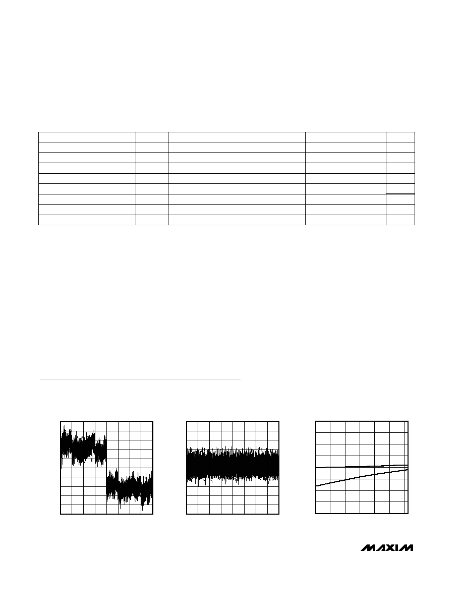
INL vs. CODE
MX7841 toc01
CODE
INL (LSB)
14336
12288
8192 10240
4096 6144
2048
-0.400
-0.300
-0.200
-0.100
0
0.100
0.200
0.300
0.400
0.500
-0.500
0
16384
DNL vs. CODE
MX7841 toc02
CODE
DNL (LSB)
14336
12288
8192 10240
4096 6144
2048
-0.400
-0.300
-0.200
-0.100
0
0.100
0.200
0.300
0.400
0.500
-0.500
0
16384
INL AND DNL ERROR
vs. TEMPERATURE
MX7841 toc03
TEMPERATURE (
∞C)
ERROR (LSB)
80
60
-20
0
20
40
-0.3
-0.2
-0.1
0
0.1
0.2
0.3
0.4
-0.4
-40
INL
DNL
MX7841
Octal, 14-Bit Voltage-Output DAC
with Parallel Interface
_______________________________________________________________________________________
5
1M
10M
-40
-35
-30
-25
-20
-10
-15
-5
0
5
1k
10k
100k
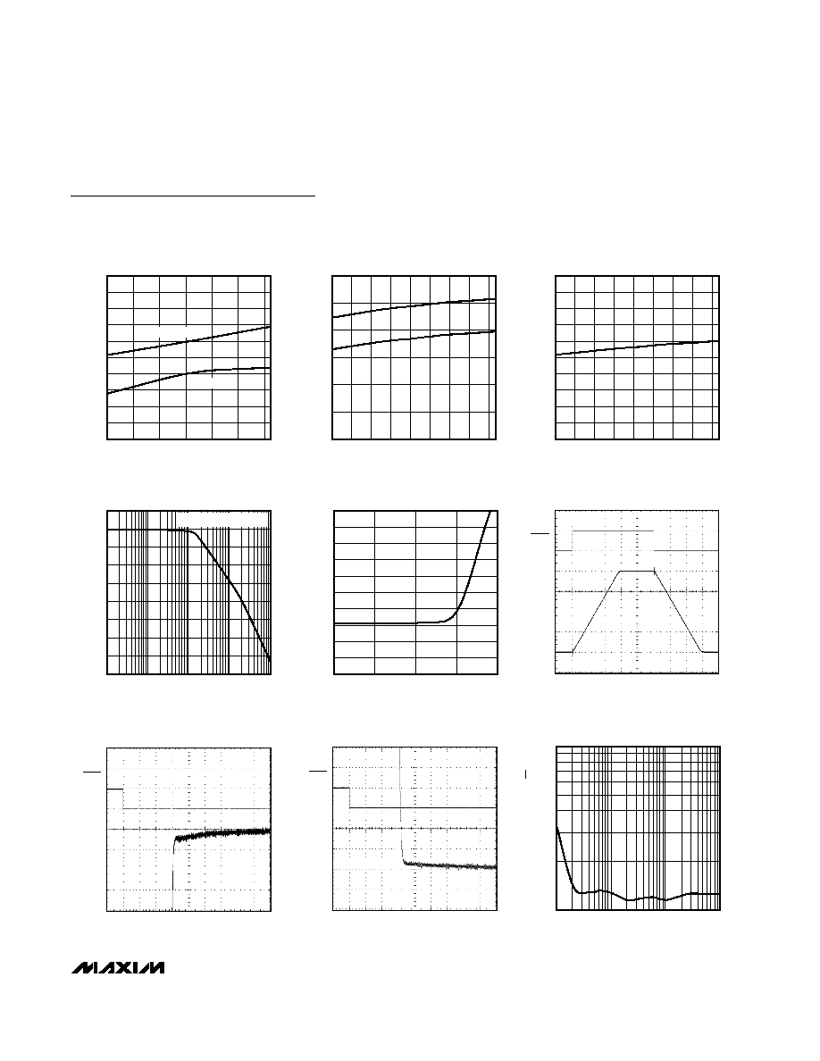
REFERENCE INPUT FREQUENCY RESPONSE
MX7841 toc07
FREQUENCY (Hz)
AMPLITUDE (dB)
REF_ _ _ _ _ = 200mVp-p
SETTLING TIME
vs. CAPACITIVE LOAD
MX7841 toc08
CAPACITIVE LOAD (pF)
SETTLING TIME (
µ
s)
10,000
1000
100
10
20
30
40
50
60
70
80
90
100
0
10
100,000
LARGE-SIGNAL STEP RESPONSE
MX7841 toc09
10
µs/div
LDAC
5V/div
OUT_
5V/div
POSITIVE SETTLING TIME
MX7841 toc10
10
µs/div
OUT_
1mV/div
LDAC
5V/div
NEGATIVE SETTLING TIME
MX7841 toc11
10
µs/div
OUT_
1mV/div
LDAC
5V/div
1000
100
10
100
1k
10k
NOISE VOLTAGE DENSITY
vs. FREQUENCY
MX7841 toc12
FREQUENCY (Hz)
NOISE VOLTAGE DENSITY (nV/
Hz)
ZERO-SCALE AND FULL-SCALE ERROR
vs. TEMPERATURE
MX7841 toc04
TEMPERATURE (
∞C)
ERROR (LSB)
80
60
20
40
0
-20
-0.6
-0.4
-0.2
0
0.2
0.4
0.6
0.8
1.0
1.2
-0.8
-40
FULL SCALE
ZERO SCALE
I
DD
AND I
SS
vs. TEMPERATURE
MX7841 toc05
TEMPERATURE (
∞C)
I
DD
, I
SS
(mA)
80
65
50
35
20
5
-10
-25
5.5
6.0
6.5
7.0
7.5
8.0
5.0
-40
IDD
ISS
DIGITAL SUPPLY CURRENT
vs. TEMPERATURE
MX7841 toc06
TEMPERATURE (
∞C)
DIGITAL SUPPLY CURRENT, I
CC
(
µ
A)
80
65
35
50
-10
5
20
-25
20.5
21.0
21.5
22.0
22.5
23.0
23.5
24.0
24.5
25.0
20.0
-40
Typical Operating Characteristics (continued)
(V
DD
= +15V ±10%, V
SS
= -15V ±10%, V
CC
= +5V ±5%, V
GND
= V
DUTGND_ _
= 0, V
REF
_ _ _ _+ = +5V, V
REF
_ _ _ _- = -5V, T
A
=
+25∞C, unless otherwise noted.)