SCOPE: PIN-PROGRAMMABLE PRECISION VOLT REFERENCE
Device Type Generic Number
01
MX584S(x)/883B
02
MX584T(x)/883B
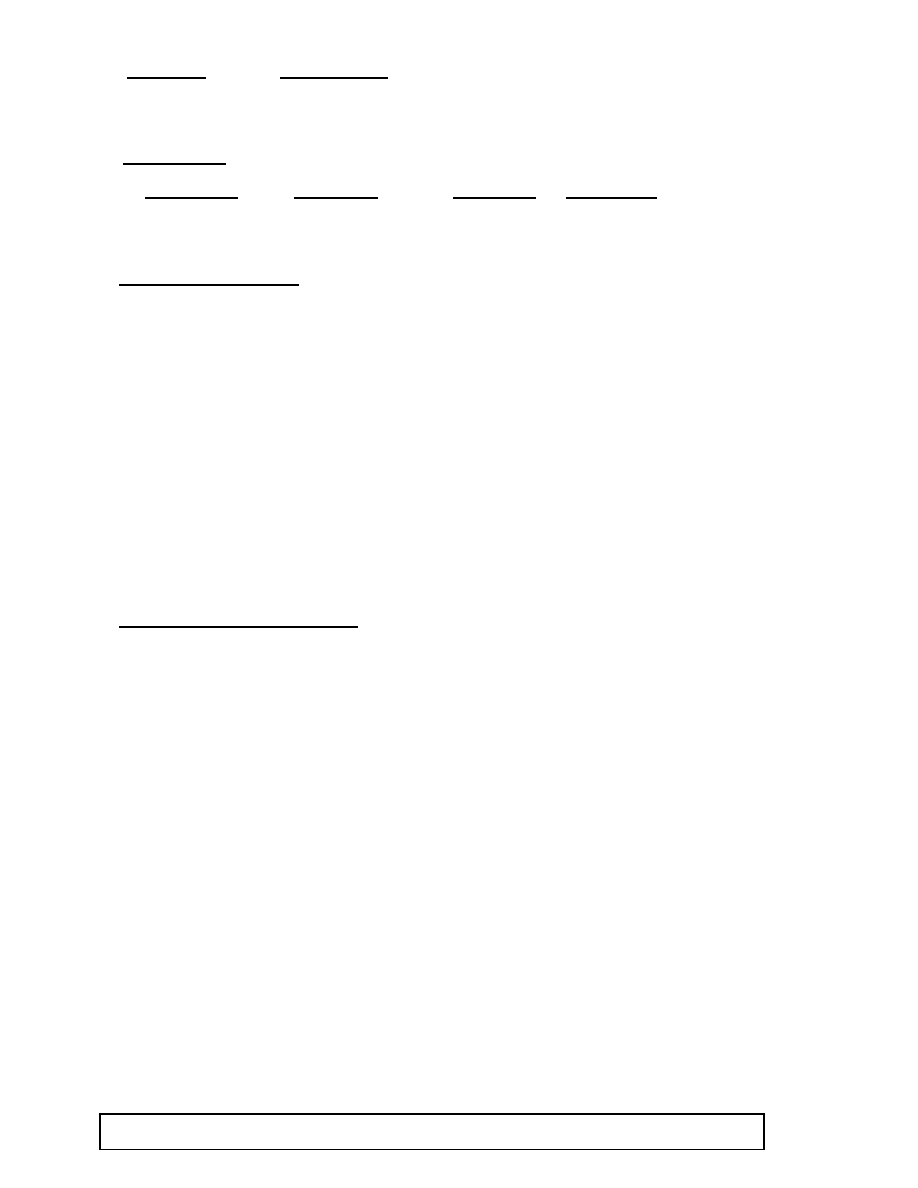
Case Outline(s). The case outlines shall be designated in Mil-Std-1835 and as follows:
Outline Letter Mil-Std-1835 Case Outline Package Code
MAXIM SMD
H G MACY1-X3 8 Lead TO-99 Can G99
Q P GDIP1-T8 or CDIP2-T8 8 Lead CERDIP J8
Absolute Maximum Ratings
Input Voltage to GND .............................................................................................. 40V
Lead Temperature (soldering, 10 seconds) .............................................................. +300
∞
C
Storage Temperature ................................................................................. -65
∞
C to +150
∞
C
Continuous Power Dissipation .............................................................................T
A
=
+
70
∞
C
8-Pin TO-99 Can(derate 6.1mW/
∞
C above +70
∞
C) ................................................ 533mW
8-Pin CERDIP(derate 8.0mW/
∞
C above +70
∞
C) .................................................... 640mW
Junction Temperature T
J
...................................................................................... +150
∞
C
Thermal Resistance, Junction to Case,
JC:
8-Pin TO-99 Can .................................................................................... 45
∞
C/W
8-Pin CERDIP ........................................................................................ 55
∞
C/W
Thermal Resistance, Junction to Ambient,
JA:
8-Pin TO-99 Can .................................................................................. 150
∞
C/W
8-Pin CERDIP ...................................................................................... 125
∞
C/W
Recommended Operating Conditions
Supply Voltage Range (V
IN
) ......................................................... 4.5V min to 30V max
Ambient Operating Range (T
A
) ........................................................... -55
∞
C to
+
125
∞
C
Stresses beyond those listed under "Absolute Maximum Ratings" may cause permanent damage to the device.
These are stress ratings only, and functional operation of the device at these or any other conditions beyond
those indicated in the operational sections of the specifications is not implied. Exposure to absolute maximum
rating conditions for extended periods may affect device reliability.
----------------------------
Electrical Characteristics of MX584S/T/883B
19-0456
Rev. C
for SMD 5962-3812803 and 5962-3812804
Page 2 of
5
TABLE 1 ELECTRICAL TESTS
TEST
Symbol
CONDITIONS
-55
∞
C
T
A
+125
∞
C
V
CC
=+15V, 10V output, I
L
=0mA
Unless otherwise specified
Group A
Subgroup
Device
type
Limits
Min
1/
Limits
Max
1/
Units
Quiescent Current
I
Q
V
IN
=38V, V
O
=10V
1
All
0
1.0 mA
Output Voltage
Error
V
OUT1
V
OUT2
V
OUT3
V
OUT4
10V Output
7.5V Output
5.0V Output
2.5V Output
1
1
1
1
01
02
01
02
01
02
01
02
9.97
9.99
7.478
7.492
4.985
4.994
2.4925
2.4965
10.03
10.01
7.522
7.508
5.015
5.006
2.5075
2.5035
mV
Line Regulation
NOTE 1
VR
LINE1
VR
LINE2
12.5V
V
IN
15V, V
O
=10V
15V
V
IN
30V, V
O
=10V
1
2,3
1
2,3
All
±
.005
±
.010
±
.002
±
.005
%/V
Load Regulation
VR
LOAD
1,2,3,4
I
L
=0mA to 5mA, Output=10V,
7.5V, 5V, 2.5V
1
2,3
All
±
50
±
100
ppm/mA
Output Short
Circuit Current
I
OS
V
O
=10V
1,2,3
All
-55 mA
Output Voltage
Temperature
Coefficient
V
OUT
1/
T
V
OUT
2/
T
V
OUT
3/
T
V
OUT
4/
T
10V Output
7.5V Output
5.0V Output
2.5V Output
2,3
2,3
2,3
2,3
01
02
01
02
01
02
01
02
±
0.3
±
0.15
±
0.3
±
0.15
±
0.3
±
0.15
±
0.3
±
0.2
%FS
Output Noise
N
O
V
O
=10V, 0.1Hz
BW
10Hz
V
O
=10V, 10Hz
BW
100H=kHz
4
All
50
150
µ
Vp-p
µ
V rms
Settling Time 0.1%
of final value
(power up)
t
S(p)
V
O
=10V, I
L
=0mA NOTE 2
V
O
=10V, I
L
=5mA NOTE 2
9
All
1000
1000
µ
s
NOTE 1: The limiting terms "min" (minimum) and "max" (maximum) shall be considered to apply to magnitudes
only. Negative current is defined as conventional currrent flow out of a device.
NOTE 2: Guaranteed, if not tested, to the limits specified in Table 1.
ORDERING INFORMATION:
Device
Maxim Part Number
SMD Number
01
MX584SH/883B
5962-3812803MGC
01
MX584SQ/883B
5962-3812803MPA
02
MX584TH/883B
5962-3812804MGC
02
MX584TQ/883B
5962-3812804MPA
----------------------------
Electrical Characteristics of MX584S/T/883B
19-0456
Rev. C
for SMD 5962-3812803 and 5962-3812804
Page 3 of
5
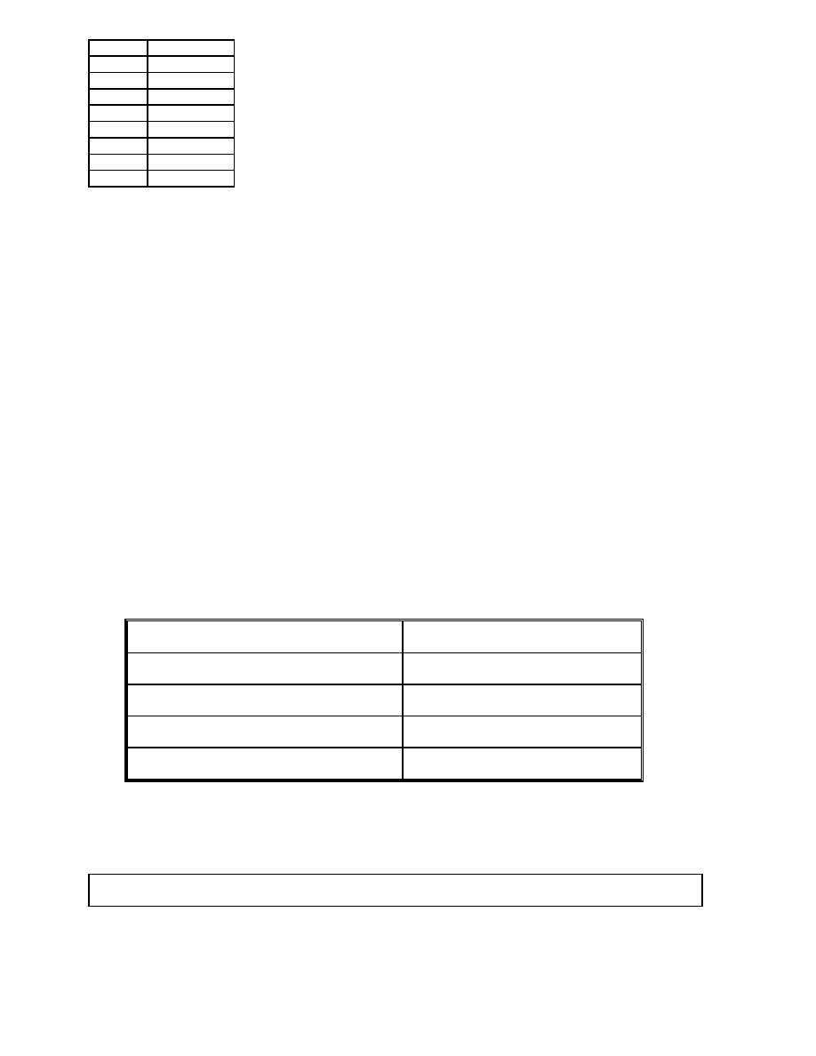
PIN CONFIGURATIONS:
PIN
J8/G99
1
10.0V
2
5.0V
3
2.5V
4
GND
5
STROBE
6
V
BG
7
CAP
8
V
CC
QUALITY ASSURANCE
Sampling and inspection procedures shall be in accordance with MIL-Prf-38535, Appendix A as specified in Mil-Std-883.
Screening shall be in accordance with Method 5004 of Mil-Std-883. Burn-in test Method 1015:
1. Test Condition, A, B, C, or D.
2. TA = +125
∞
C minimum.
3. Interim and final electrical test requirements shall be specified in Table 2.
Quality conformance inspection shall be in accordance with Method 5005 of Mil-Std-883, including Groups A, B, C, and D
inspection.
Group A inspection:
1. Tests as specified in Table 2.
2. Selected subgroups in Table 1, Method 5005 of Mil-Std-883 shall be omitted.
Group C and D inspections:
a. End-point electrical parameters shall be specified in Table 1.
b. Steady-state life test, Method 1005 of Mil-Std-883:
1. Test condition A, B, C, D.
2. TA = +125
∞
C, minimum.
3. Test duration, 1000 hours, except as permitted by Method 1005 of Mil-Std-883.
TABLE 2. ELECTRICAL TEST REQUIREMENTS
Mil-Std-883 Test Requirements
Subgroups
per Method 5005, Table 1
Interim Electric Parameters
Method 5004
1
Final Electrical Parameters
Method 5005
1*, 2, 3, 4, 9
Group A Test Requirements
Method 5005
1, 2, 3, 4, 9
Group C and D End-Point Electrical Parameters
Method 5005
1
* PDA applies to Subgroup 1 only.
----------------------------
Electrical Characteristics of MX584S/T/883B
19-0456
Rev. C
for SMD 5962-3812803 and 5962-3812804
Page 4 of
5