
SCOPE: CMOS HIGHSPEED 8-BIT A/D CONVERTER WITH TRACK AND HOLD
Device Type Generic Number
01 MX7828T(x)/883B
02 MX7828U(x)/883B
Case Outline(s). The case outlines shall be designated in Mil-Std-1835 and as follows:
Outline Letter Mil-Std-1835 Case Outline Package Code
MAXIM SMD
Q X GDIP1-T28 or CDIP2-T28 28 LEAD CERDIP J28
Absolute Maximum Ratings
Supply Voltage to GND ..................................................................................... 0V, +7V
__ __
Digital Input Voltage to GND (RD, CS, A0, A1, A2) ................................... -0.3V, V
DD
___
Digital Output Voltage to GND (D0-D7, RDY, INT) .................................... -0.3V, V
DD
Positive Reference Voltage ....................................................................... VREF- to V
DD
Negative Reference Voltage ...................................................................... 0V to VREF+
Input Voltage (V
IN
) ..................................................................................... -0.3V to V
DD
Lead Temperature (soldering, 10 seconds) ................................................................ +300
∞
C
Storage Temperature ................................................................................... -65
∞
C to +150
∞
C
Continuous Power Dissipation ............................................................................. T
A
=
+
70
∞
C
28 pin CERDIP(derate 16.67mW/
∞
C above +70
∞
C) ................................................ 1333mW
Junction Temperature T
J
......................................................................................... +150
∞
C
Thermal Resistance, Junction to Case,
JC
28 pin CERDIP..................................................................................................... 25
∞
C/W
Thermal Resistance, Junction to Ambient,
JA:
28 pin CERDIP.................................................................................................... 60
∞
C/W
Recommended Operating Conditions
Ambient Operating Range (T
A
) ............................................................. -55
∞
C to
+
125
∞
C
Supply Voltage Range (V
DD
) ................................................................. +4.75V to +5.25V
Positive Reference Voltage (VREF+) ....................................................................... +5.0V
Negative Reference Voltage (VREF-) ........................................................................... 0V
Ground Potential (GND) ............................................................................................... 0V
Stresses beyond those listed under "Absolute Maximum Ratings" may cause permanent damage to the device.
These are stress ratings only, and functional operation of the device at these or any other conditions beyond
those indicated in the operational sections of the specifications is not implied. Exposure to absolute maximum
rating conditions for extended periods may affect device reliability.
----------------------------
Electrical Characteristics of MX7828/883B
19-1038
Rev. C
for /883B and SMD 5962-8876403 and 04
Page 2 of
9

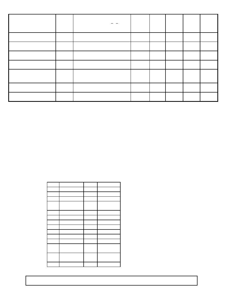
TABLE 1. ELECTRICAL TESTS:
TEST
Symbol
CONDITIONS
-55
∞
C
T
A
+125
∞
C 1/ 2/
Unless otherwise specified
Group A
Subgroup
Device
type
Limits
Min
Limits
Max
Units
Resolution
RES
Guaranteed but not tested
1,2,3
All
8
LSB
Total Unadjusted Error
NOTE 3
TUE
1,2,3
01
02
±
1.0
±
0.5
LSB
Analog Input Voltage
Range
V
IN
1
All
VREF-
VREF+ V
Analog Input Leakage
Current
I
IN
Any channel
1,2,3
All
-3.0
+3.0
µ
A
Analog Input Capacitance
C
IN1
0V, 5V, NOTE 4
4
All
45 pF
Reference Input Resistance
R
IN
NOTE 4
1,2,3
All
1.0
4.0 k
Digital Input High Level
Voltage
V
IH
___ __
A0, A1, A2, RD, CS
1,2,3
All
2.4
V
Digital Input Low Level
Voltage
V
IL
___ __
A0, A1, A2, RD, CS
1,2,3
All
0.8 V
Digital Input High Current
I
IH
___ __
A0, A1, A2, RD, CS
1,2,3
All
+1.0
µ
A
Digital Input Low Current
I
IL
___ __
A0, A1, A2, RD, CS
1,2,3
All
-1.0
µ
A
Digital Input Capacitance
C
IN2
___ __ NOTE 4
A0, A1, A2, RD, CS
4
All
8.0 pF
Digital Output High Level
Voltage
V
OH
___
DB0-DB7, INT, I
SOURCE
=360
µ
A
1,2,3
All
4.0
V
Digital Output Low Level
Voltage
V
OL
___
DB0-DB7, INT, I
SINK
=1.6mA
RDY, I
SINK
=2.6mA, NOTE 5
1,2,3
All
0.4
0.4
V
Floating State Leakage
Current
I
OUT
DB0-DB7 only
1,2,3
All
±
3.0
µ
A
Slew Rate, Tracking
Capacitance NOTE 4
4
All
0.157 V/
µ
s
Digital Output Capacitance
C
OUT
NOTE 4
4
All
8.0 pF
Supply Current
I
DD
__ ___
CS=RD=2.4V
1,2,3
All
20.0 mA
Power Supply Sensitivity
PSS
V
DD
=5.0V
±
5%
1,2,3
All
±
0.25 LSB
__ __
CS to RD Setup Time
t
CSS
Figure 3
9,10,11
All
0
ns
__ __
CS to RD Hold Time
t
CSH
Figure 3
9,10,11
All
0
ns
__
CS to RDY delay
t
RDY
Pull-up resistor=5k
, CL=50pF,
Figure 3
9
10,11
All
40
60
ns
Conversion Time, Mode 0
t
CRD
See Figure 3. NOTE 7
9
10,11
All
2.0
2.8
µ
s
Data Access Time __
After RD,
Mode 1
t
ACC1
NOTE 6 and 7
Figure 3 and 5
9
10,11
All
85
120
ns
----------------------------
Electrical Characteristics of MX7828/883B
19-1038
Rev. C
for /883B and SMD 5962-8876403 and 04
Page 3 of
9
TEST
Symbol
CONDITIONS
-55
∞
C
T
A
+125
∞
C 1/ 2/
Unless otherwise specified
Group A
Subgroup
Device
type
Limits
Min
Limits
Max
Units
__ ___
RD to INT Delay, NOTE 5
t
INTH
CL=50pF
9
10,11
All
75
100
ns
Data Hold Time
t
DH
NOTE 8, Figure 3,4
9
10,11
All
60
70
ns
Delay Time Between
Conversion
t
P
Figure 3
9
10,11
All
500
600
ns
Read Pulse Width, Mode 1
t
RD
Figure 3
9
10,11
All
60
80
600
400
ns
Data Access Time After
___
INT, Mode 0
t
ACC2
NOTE 6, 7, Figure 3,5
9
10,11
All
50
70
ns
Multiplexer Address Setup
Time
t
AS
Figure 3
9,10,11
All
0
ns
Multiplexer Address Hold
Time
t
AH
Figure 3
9
10,11
All
30
40
ns
NOTE 1: V
DD
=+5V, VREF(+)=+5V; VREF(-)=GND=0V, unless otherwise specified.
Specifications apply for mode 0. All input control signals are specified with tr=tf=20ns
(10 percent to 90 percent of +5.0V) and timed from a voltage level of 1.6V.
NOTE 2: Subgroups 10 and 11, if not tested, shall be guaranteed to the limits specified in Table 1.
NOTE 3: Total unadjusted error includes offset, full-scale, and linearity errors.
NOTE 4: The (C
IN1
, C
IN2
, R
IN
, C
OUT
, and S
R
measurements) are measured initially and after any process
or design changes which may affect these tests.
NOTE 5: RDY is an open-drain output.
NOTE 6: Measured with load circuits of Figure 5 and defined as the time required for an output to
cross 0.8V or 2.4V.
NOTE 7: If not tested, it shall be guaranteed to the limits specified in Table 1.
NOTE 8: Defined as the time required for the data lines to change 0.5V when loaded with the circuits of
Figure 4 and is measured only for the initial test and after process or design change which may
affect t
DH
.
TERMINAL CONNECTIONS
J28
J28
1
AIN6
15
VREF-
2
AIN5
16
VREF+
3
AIN4
17
RDY
4
AIN3
18
__
CS
5
AIN2
19
D4
6
AIN1
20
D5
7
NC
21
D6
8
D0
22
D7
9
D1
23
A2
10
D2
24
A1
11
D3
25
A0
12
__
RD
26
V
DD
13
___
INT
27
AIN8
14
GND
28
AIN7
----------------------------
Electrical Characteristics of MX7828/883B
19-1038
Rev. C
for /883B and SMD 5962-8876403 and 04
Page 4 of
9
Package
ORDERING INFORMATION:
SMD NUMBER
01
28 pin CERDIP
MX7828TQ/883B
5962-8876403LA
02
28 pin CERDIP
MX7828UQ/883B
5962-8876404LA
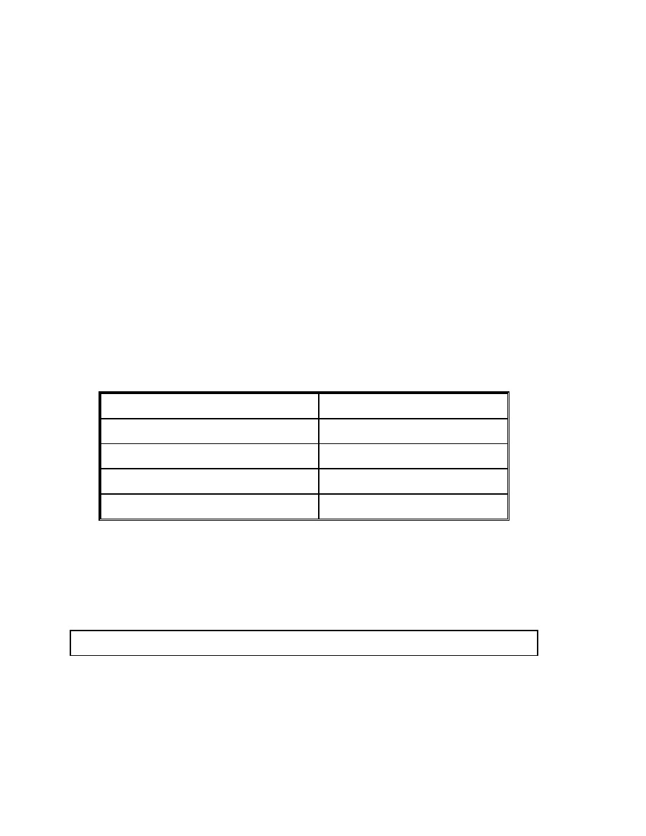
MODE SELECTION TABLE
CHANNEL
A2
A1
A0
AIN1
0
0
0
AIN2
0
0
1
AIN3
0
1
0
AIN4
0
1
1
AIN5
1
0
0
AIN6
1
0
1
AIN7
1
1
0
AIN8
1
1
1
----------------------------
Electrical Characteristics of MX7828/883B
19-1038
Rev. C
for /883B and SMD 5962-8876403 and 04
Page 5 of
9
QUALITY ASSURANCE
Sampling and inspection procedures shall be in accordance with MIL-Prf-38535, Appendix A as specified in Mil-
Std-883.
Screening shall be in accordance with Method 5004 of Mil-Std-883. Burn-in test Method 1015:
1. Test Condition, A, B, C, or D.
2. TA = +125
∞
C minimum.
3. Interim and final electrical test requirements shall be specified in Table 2.
Quality conformance inspection shall be in accordance with Method 5005 of Mil-Std-883, including Groups A, B,
C, and D inspection.
Group A inspection:
1. Tests as specified in Table 2.
2. Selected subgroups in Table 1, Method 5005 of Mil-Std-883 shall be omitted.
Group C and D inspections:
a. End-point electrical parameters shall be specified in Table 1.
b. Steady-state life test, Method 1005 of Mil-Std-883:
1. Test condition A, B, C, D.
2. TA = +125
∞
C, minimum.
3. Test duration, 1000 hours, except as permitted by Method 1005 of Mil-Std-883.
TABLE 2. ELECTRICAL TEST REQUIREMENTS
Mil-Std-883 Test Requirements
Subgroups
per Method 5005, Table 1
Interim Electric Parameters
Method 5004
1
Final Electrical Parameters
Method 5005
1*, 2, 3, 4**, 9, 10, 11***
Group A Test Requirements
Method 5005
1, 2, 3, 4**, 9, 10, 11***
Group C and D End-Point Electrical Parameters
Method 5005
1
* PDA applies to Subgroup 1 only.
** Subgroup 4, Capacitance tests are performed at initial qual and upon redesign.
Sample size will be 116 units.
*** Subgroups 10 and 11 if not tested, are guaranteed to the limits specified in Table 1.
----------------------------
Electrical Characteristics of MX7828/883B
19-1038
Rev. C
for /883B and SMD 5962-8876403 and 04
Page 8 of
9