1
M
e
m
o
r
y
All data sheets are subject to change without notice
(858) 503-3300- Fax: (858) 503-3301 - www.maxwell.com
1 Megabit (128K x 8-Bit) EEPROM
28C010T
©2003 Maxwell Technologies
All rights reserved.
06.03.03 REV 14
F
EATURES
:
∑ 128k x 8-bit EEPROM
∑ R
AD
-P
AK
Æ radiation-hardened against natural space radia-
tion
∑ Total dose hardness:
- > 100 krad (Si), depending upon space mission
∑ Excellent Single event effects
- SEL
TH
> 120 MeV/mg/cm
2
- SEU > 90 MeV/mg/cm
2
read mode
- SEU = 18 MeV/mg/cm
2
write mode
∑ Package:
- 32-pin R
AD
-P
AK
Æ flat pack/DIP package
- JEDEC-approved byte-wide pinout
∑ High speed:
- 120, 150, and 200 ns maximum access times available
∑ High endurance:
- 10,000 erase/write (in Page Mode),
- 10 year data retention
∑ Page write mode:
- 1 to 128 bytes
∑ Low power dissipation
- 20 mW/MHz active (typical)
- 110 µ W standby (maximum)
∑ Standard JEDEC package width
D
ESCRIPTION
:
Maxwell Technologies' 28C010T high-density 1 Megabit
(128K x 8-Bit) EEPROM microcircuit features a greater than
100 krad (Si) total dose tolerance, depending upon space mis-
sion. The 28C010T is capable of in-system electrical byte and
page programmability. It has a 128-byte page programming
function to make its erase and write operations faster. It also
features data polling and a Ready/Busy signal to indicate the
completion of erase and programming operations. In the
28C010T, hardware data protection is provided with the RES
pin, in addition to noise protection on the WE signal and write
inhibit on power on and off. Software data protection is imple-
mented using the JEDEC optional standard algorithm.
Maxwell Technologies' patented R
AD
-P
AK
Æ packaging technol-
ogy incorporates radiation shielding in the microcircuit pack-
age. It eliminates the need for box shielding while providing
the required radiation shielding for a lifetime in orbit or space
mission. In a GEO orbit, R
AD
-P
AK
Æ provides greater than 100
krad(Si) radiation dose tolerance. This product is available
with screening up to Class S.
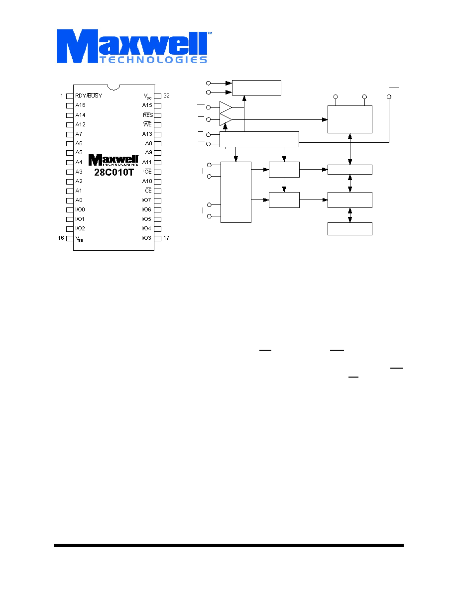
High Voltage
Generator
Control Logic Timing
Address
Buffer and
Latch
Y Decoder
X Decoder
Y Gating
Memory Array
I/O Buffer and
Input Latch
Data Latch
V
CC
V
SS
RES
OE
CE
WE
RES
A0
A6
A7
A16
I/O0
I/O7
RDY/Busy
Logic Diagram

M
e
m
o
r
y
2
All data sheets are subject to change without notice
©2003 Maxwell Technologies
All rights reserved.
1 Megabit (128K x 8-Bit) EEPROM
28C010T
06.03.03 REV 14
T
ABLE
1. 28C010T P
INOUT
D
ESCRIPTION
P
IN
S
YMBOL
D
ESCRIPTION
12-5, 27, 26, 23, 25, 4, 28, 3, 31, 2
A0-A16
Address
13, 14, 15, 17, 18, 19, 20, 21
I/O0 - I/O7
Data I/O
24
OE
Output Enable
22
CE
Chip Enable
29
WE
Write Enable
32
V
CC
Power Supply
16
V
SS
Ground
1
RDY/BUSY
Ready/Busy
30
RES
Reset
T
ABLE
2. 28C010T A
BSOLUTE
M
AXIMUM
R
ATINGS
P
ARAMETER
S
YMBOL
M
IN
T
YP
M
AX
U
NITS
Supply Voltage (Relative to V
SS
)
V
CC
-0.6
+7.0
V
Input Voltage (Relative to V
SS
)
V
IN
-0.5
1
1. V
IN
min = -3.0V for pulse width < 50ns.
+7.0
V
Package Weight
RP
7.4
Grams
RT
2.7
RD
10.9
Thermal Impedance (RP and RT Packages)
F
JC
2.4
∞
C/W
Thermal Impedance (DIP Package)
F
JC
2.17
∞
C/W
Operating Temperature Range
T
OPR
-55
+125
∞
C
Storage Temperature Range
T
STG
-65
+150
∞
C
T
ABLE
3. D
ELTA
L
IMITS1
1. Parameters are measured and recorded as Deltas per
MIL-STD-883 for Class S Devices
P
ARAMETER
V
ARIATION2
2. Specified in Table 6
I
CC1
±10%
I
CC2
±10%
I
CC3A
±10%
I
CC3B
±10%
M
e
m
o
r
y
3
All data sheets are subject to change without notice
©2003 Maxwell Technologies
All rights reserved.
1 Megabit (128K x 8-Bit) EEPROM
28C010T
06.03.03 REV 14
T
ABLE
4. 28C010T R
ECOMMENDED
O
PERATING
C
ONDITIONS
P
ARAMETER
S
YMBOL
M
IN
M
AX
U
NITS
Supply Voltage
V
CC
4.5
5.5
V
Input Voltage
RES_PIN
V
IL
-0.3
1
1. V
IL
min = -1.0V for pulse width < 50 ns
0.8
V
V
IH
2.2
V
CC
+0.3
V
H
V
CC
-0.5
V
CC
+1
T
ABLE
5. 28C010T C
APACITANCE
(T
A
= 25
∞
C, f = 1 MHZ)
P
ARAMETER
S
YMBOL
M
IN
M
AX
U
NITS
Input Capacitance: V
IN
= 0V
1
1. Guaranteed by design.
C
IN
--
6
pF
Output Capacitance: V
OUT
= 0V
1
C
OUT
--
12
pF
T
ABLE
6. 28C010T DC E
LECTRICAL
C
HARACTERISTICS
(V
CC
= 5V ± 10%, T
A
= -55
TO
+125
∞
C,
UNLESS
OTHERWISE
SPECIFIED
)
P
ARAMETER
T
EST
C
ONDITION
S
UBGROUPS
S
YMBOL
M
IN
M
AX
U
NITS
Input Leakage Current
V
CC
= 5.5V, V
IN
= 5.5V
1, 2, 3
I
IL
--
2
1
1. I
LI
for RES = 100uA max.
µ A
Output Leakage Current
V
CC
= 5.5V, V
OUT
= 5.5V/0.4V
1, 2, 3
I
LO
--
2
µ A
Standby V
CC
Current
CE = V
CC
1, 2, 3
I
CC1
--
20
µ A
CE = V
IH
I
CC2
--
1
mA
Operating V
CC
Current
I
OUT
= 0mA, Duty = 100%,
Cycle = 1µ s at V
CC
= 5.5V
1, 2, 3
I
CC3A
--
15
mA
I
OUT
= 0mA, Duty = 100%,
Cycle = 150ns at V
CC
= 5.5V
1, 2, 3
I
CC3B
--
50
Input Voltage
RES_PIN
1, 2, 3
V
IL
--
0.8
V
V
IH
2.2
--
V
H
V
CC
-0.5
--
Output Voltage
2
2. RDY/BSY is an open drain output. Only V
OL
applies to this pin.
I
OL
= 2.1 mA
1, 2, 3
V
OL
--
0.4
V
I
OH
= - 0.4 mA
V
OH
2.4
--
I
OH
= - 0.1 mA
V
OH
V
CC
-0.3V

M
e
m
o
r
y
4
All data sheets are subject to change without notice
©2003 Maxwell Technologies
All rights reserved.
1 Megabit (128K x 8-Bit) EEPROM
28C010T
06.03.03 REV 14
T
ABLE
7. 28C010T AC E
LECTRICAL
C
HARACTERISTICS
FOR
R
EAD
O
PERATION
1
(V
CC
= 5V + 10%, T
A
= -55
TO
+125
∞
C)
1. Test conditions: Input pulse levels - 0.4V to 2.4V; input rise and fall times < 20ns; output load - 1 TTL gate + 100pF (including
scope and jig); reference levels for measuring timing - 0.8V/1.8V.
P
ARAMETER
S
YMBOL
S
UBGROUPS
M
IN
M
AX
U
NITS
Address Access Time
CE = OE = V
IL
, WE = V
IH
-120
-150
-200
t
ACC
9, 10, 11
--
--
--
120
150
200
ns
Chip Enable Access Time
OE = V
IL
, WE = V
IH
-120
-150
-200
t
CE
9, 10, 11
--
--
--
120
150
200
ns
Output Enable Access Time
CE = V
IL
, WE = V
IH
-120
-150
-200
t
OE
9, 10, 11
0
0
0
75
75
100
ns
Output Hold to Address Change
CE = OE = V
IL
, WE = V
IH
-120
-150
-200
t
OH
9, 10, 11
0
0
0
--
--
--
ns
Output Disable to High-Z
2
CE = V
IL
, WE = V
IH
-120
-150
-200
CE = OE = V
IL
, WE = V
IH
-120
-150
-200
2. t
DF
and t
DFR
are defined as the time at which the output becomes an open circuit and data is no longer driven.
t
DF
t
DFR
9, 10, 11
0
0
0
0
0
0
50
50
60
300
350
450
ns
RES to Output Delay
3
CE = OE = V
IL
, WE = V
IH
-120
-150
-200
3. Guaranteed by design.
t
RR
9, 10, 11
--
--
--
400
450
650
ns

M
e
m
o
r
y
5
All data sheets are subject to change without notice
©2003 Maxwell Technologies
All rights reserved.
1 Megabit (128K x 8-Bit) EEPROM
28C010T
06.03.03 REV 14
T
ABLE
8. 28C010T AC E
LECTRICAL
C
HARACTERISTICS
FOR
P
AGE
/B
YTE
E
RASE
AND
P
AGE
/B
YTE
W
RITE
O
PERATIONS
(V
CC
= 5V + 10%, T
A
= -55
TO
+125
∞
C)
P
ARAMETER
S
YMBOL
S
UBGROUPS
M
IN
1
M
AX
U
NITS
Address Setup Time
-120
-150
-200
t
AS
9, 10, 11
0
0
0
--
--
--
ns
Chip Enable to Write Setup Time (WE controlled)
-120
-150
-200
t
CS
9, 10, 11
0
0
0
--
--
--
ns
Write Pulse Width
CE controlled
-120
-150
-200
WE controlled
-120
-150
-200
t
CW
t
WP
9, 10, 11
200
250
350
200
250
350
--
--
--
--
--
--
ns
Address Hold Time
-120
-150
-200
t
AH
9, 10, 11
150
150
200
--
--
--
ns
Data Setup Time
-120
-150
-200
t
DS
9, 10, 11
75
100
150
--
--
--
ns
Data Hold Time
-120
-150
-200
t
DH
9, 10, 11
10
10
10
--
--
--
ns
Chip Enable Hold Time (WE controlled)
-120
-150
-2000
t
CH
9, 10, 11
0
0
0
--
--
--
ns
Write Enable to Write Setup Time (CE controlled)
-120
-150
-200
t
WS
9, 10, 11
0
0
0
--
--
--
ns
Write Enable Hold Time (CE controlled)
-120
-150
-200
t
WH
9, 10, 11
0
0
0
--
--
--
ns