1
Memory
All data sheets are subject to change without notice
(858) 503-3300 - Fax: (858) 503-3301 - www.maxwell.com
P
RELIMINARY
3.3V ABT Octal Bus Transceiver
54LVTH245A
©2001 Maxwell Technologies
All rights reserved.
with 3-State Output
12.19.01 Rev 1
1000597
F
EATURES
:
∑ 3.3V ABT octal bus transceiver with 3-state outputs
∑ R
AD
-P
AK
Æ radiation hardened against natural space radia-
tion
∑ Total dose hardness:
- >100 krad (Si), depending upon space misssion
∑ Package:
- 20 pin R
AD
-P
AK
Æ flat package
- 20 pin R
AD
-P
AK
Æ DIP
∑ Operating temperature range:
-55 to 125
∞
C
∑ Supports mixed-mode signal operation
- 5V input and output voltages with 3.3V V
CC
∑ Supports unregulated battery operation down to 2.7V.
∑ Typical VOLP (output ground bounce) < 0.8V at V
CC
=3.3V,
T
A
= 25
∞
C
∑ Latch-up performance exceeds 500mA per JEDEC stan-
dard
∑ Supports live insertion
∑ Bus-hold data inputs eliminate the need for external pullup
resistors
D
ESCRIPTION
:
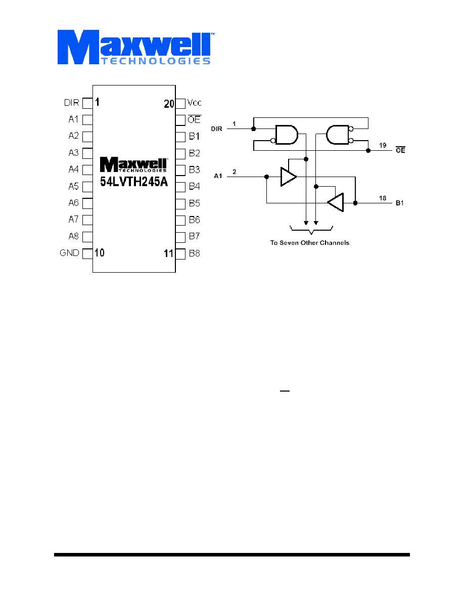
Maxwell Technologies' 54LVTH245A 8-bit octal transceiver
micro-circuit features a greater than 100 krad (Si) total dose
tolerance, depending upon space mission. The 54LVTH245A
is designed specifically for low voltage (3.3V) V
CC
operation,
but with the capability to provide a TTL interface to a 5V sys-
tem environment. It is designed for asynchronous communica-
tion between data buses. The device transmits data from the
A bus to the B bus or from the B bus to the A bus depending
upon the logic level at the direction control (DIR) input. The
output enable (OE) input can be used to disable the device so
the buses are effectively isolated. The 54LVTH245A active
bus-hold circuitry is provided to prevent floating data inputs at
a valid logic level and to eliminate the need for external pullup
resistors.
Maxwell Technologies' patented R
AD
-P
AK
Æ packaging technol-
ogy incorporates radiation shielding in the microcircuit pack-
age. It eliminates the need for box shielding while providing
the required radiation shielding for a lifetime in orbit or space
mission. In a GEO orbit, R
AD
-P
AK
provides greater than 100
krad (Si) radiation dose tolerance. This product is available
with screening up to Class S.
Logic Diagram (Positive Logic)

Memory
P
RELIMINARY
2
All data sheets are subject to change without notice
©2001 Maxwell Technologies
All rights reserved.
3.3V ABT Octal Bus Transceiver
with 3-State Output
54LVTH245A
12.19.01 Rev 1
1000597
T
ABLE
1. P
INOUT
D
ESCRIPTION
P
IN
S
YMBOL
D
ESCRIPTION
1
DIR
DirectionControl
2-9
A1-A8
Inputs
10
GND
Ground
11-18
B8-B1
Outputs
19
OE
Output Enable
20
V
CC
Supply Voltage
T
ABLE
2. 54LVT245 A
BSOLUTE
M
AXIMUM
R
ATINGS
1
1. Stresses beyond those listed under "absolute maximum ratings" may cause permanent damage to the device. These are
stress ratings only, and functional operation of the device at these or any other conditions beyond those indicated under "rec-
ommended operating conditions" is not implied. Exposure to absolute-maximum-rated conditions for extended periods may
affect device reliability.
P
ARAMETER
S
YMBOL
M
IN
M
AX
U
NIT
Supply Voltage Range
V
CC
-0.5
4.6
V
Input Voltage Range
2
2. The input and output negative-voltage ratings may be exceeded if the input and output clamp-current ratings are observed.
V
I
-0.5
7.0
V
Voltage Range Applied to Any Output in the High State or Power-Off
State
V
O
-0.5
7.0
V
Current Into Any Output in the High State
3
3. This current flows only when the output is in the high state and V
O
> V
CC
.
I
O
--
48
mA
Input Clamp Current (V
I
< 0)
I
IK
--
-50
mA
Output Clamp Current (V
O
< 0)
I
OK
--
-50
mA
Maximum Power Dissipation at T
A
= 55
∞
C
P
D
--
1.6
mW
Operating Temperature
T
A
-55
125
∞C
Storage Temperature Range
T
S
-65
150
∞
C
T
ABLE
3. D
ELTA
L
IMITS
P
ARAMETER
V
ARIATION
I
CC(OL)
±10% of specified value in Table 5
I
CC(OH)
±10% of specified value in Table 5
I
CC(OD)
±10% of specified value in Table 5

Memory
P
RELIMINARY
3
All data sheets are subject to change without notice
©2001 Maxwell Technologies
All rights reserved.
3.3V ABT Octal Bus Transceiver
with 3-State Output
54LVTH245A
12.19.01 Rev 1
1000597
T
ABLE
4. 54LVTH245A R
ECOMMENDED
O
PERATING
C
ONDITIONS
1
1. Unused control inputs must be held high or low to prevent them from floating.
P
ARAMETER
S
YMBOL
M
IN
M
AX
U
NIT
Supply Voltage
V
CC
2.7
3.6
V
High-level Input Voltage
V
IH
2.0
--
V
Low-level Input Voltage
V
IL
--
0.8
V
Input Voltage
V
I
--
5.5
V
High-level Output Current
I
OH
--
-24
mA
Low-level Output Current
I
OL
--
48
mA
Input Transition Rise or Fall Rate
Outputs
enabled
t/
v
--
10
ns/V
Operating Temperature
T
A
-55
125
∞
C
T
ABLE
5. 54LVTH245A E
LECTRICAL
C
HARACTERISTICS
(V
CC
= 3.3V ±10%, T
A
= -55 to +125∞C,
UNLESS
OTHERWISE
SPECIFIED
)
P
ARAMETER
S
YMBOL
T
EST
C
ONDITIONS
M
IN
M
AX
U
NIT
Input Clamp Voltage
V
IK
V
CC
= 2.7
I
I
= -18mA
--
-1.2
V
High-Level Output Voltage
V
OH
V
CC
= 2.7V to 3.6V
I
OH
= -100µA
V
CC
-0.2
--
V
V
CC
= 2.7V
I
OH
= -8mA
2.4
--
V
CC
= 3V,
I
OH
= -24mA
2.0
--
Low-Level Output Voltage
V
OL
V
CC
= 2.7V
I
OL
= 100µA
--
0.2
V
I
OL
= 24mA
--
0.5
V
CC
= 3V
I
OL
= 16mA
--
0.4
I
OL
= 32mA
--
0.5
I
OL
= 48mA
--
0.55
Input Current
I
I
V
CC
= 3.6V
V
I
= V
CC
or GND
Control inputs
--
±1
µA
V
CC
= 0 or 3.6V
V
I
= 5.5V
--
10
V
CC
= 3.6V
V
I
= 5.5V
A or B Ports
--
20
V
I
= V
CC
1
V
I
= 0
--
-5
Hold Current
I
I(HOLD)
V
CC
= 3V
V
I
= 0.8V
A or B Ports
75
--
µA
V
I
= 2V
-75
--
Power Up Current
I
OZPU
2
V
CC
= 0 to 1.5V, V
O
= 0.5V to 3V, OE = don't care
--
±100
µA
Power Down Current
I
OZPD
2
V
CC
= 1.5V to 0, V
O
= 0.5V to 3V, OE = don't care
--
±100
µA

Memory
P
RELIMINARY
4
All data sheets are subject to change without notice
©2001 Maxwell Technologies
All rights reserved.
3.3V ABT Octal Bus Transceiver
with 3-State Output
54LVTH245A
12.19.01 Rev 1
1000597
Supply Current
I
CC
V
CC
= 3.6V
Outputs high
--
0.39
mA
I
O
= 0
Outputs low
--
14
V
I
= V
CC
or GND
Outputs disabled
--
0.39
Delta Supply Current
I
CC
1
V
CC
= 3V to 3.6V, One input at V
CC
-0.6V, Other inputs at
V
CC
or GND
--
0.2
mA
Input Capacitance
C
I
2
V
I
= 3V or 0
--
8
pF
Input Output Capacitance
C
O
2
V
O
= 3V or 0
--
15
pF
1. This is the increase in supply current for each input that is at the specified TTL voltage level rather than V
CC
or GND.
2. Guaranteed by design.
T
ABLE
6. 54LVTH245A AC E
LECTRICAL
C
HARACTERISTICS
(V
CC
= 3.3V ±10%, T
A
= -55
RO
125∞C,
UNLESS
OTHERWISE
NOTED
)
P
ARAMETER
S
YMBOL
V
CC
= 3.3V ± 0.3V
V
CC
= 2.7V
U
NIT
M
IN
M
AX
M
IN
M
AX
Propagation Delay Time
A orB to B or A
t
PLH
0.7
3.7
--
4.2
ns
t
PHL
0.7
3.7
--
4.2
Output Enable Time
OE to A or B
t
PZH
1.2
5.7
--
7.4
ns
t
PZL
1.6
5.7
--
6.8
Output Disable Time
OE to A or B
t
PHZ
1.8
6.2
--
6.8
ns
t
PLZ
1.8
5.3
--
5.5
T
ABLE
7. F
UNCTION
T
ABLE
INPUTS
OPERATION
OE
DIR
L
L
B data to A bus
l
H
A data to B bus
H
X
Isolation
T
ABLE
5. 54LVTH245A E
LECTRICAL
C
HARACTERISTICS
(V
CC
= 3.3V ±10%, T
A
= -55 to +125∞C,
UNLESS
OTHERWISE
SPECIFIED
)
P
ARAMETER
S
YMBOL
T
EST
C
ONDITIONS
M
IN
M
AX
U
NIT
Memory
P
RELIMINARY
5
All data sheets are subject to change without notice
©2001 Maxwell Technologies
All rights reserved.
3.3V ABT Octal Bus Transceiver
with 3-State Output
54LVTH245A
12.19.01 Rev 1
1000597
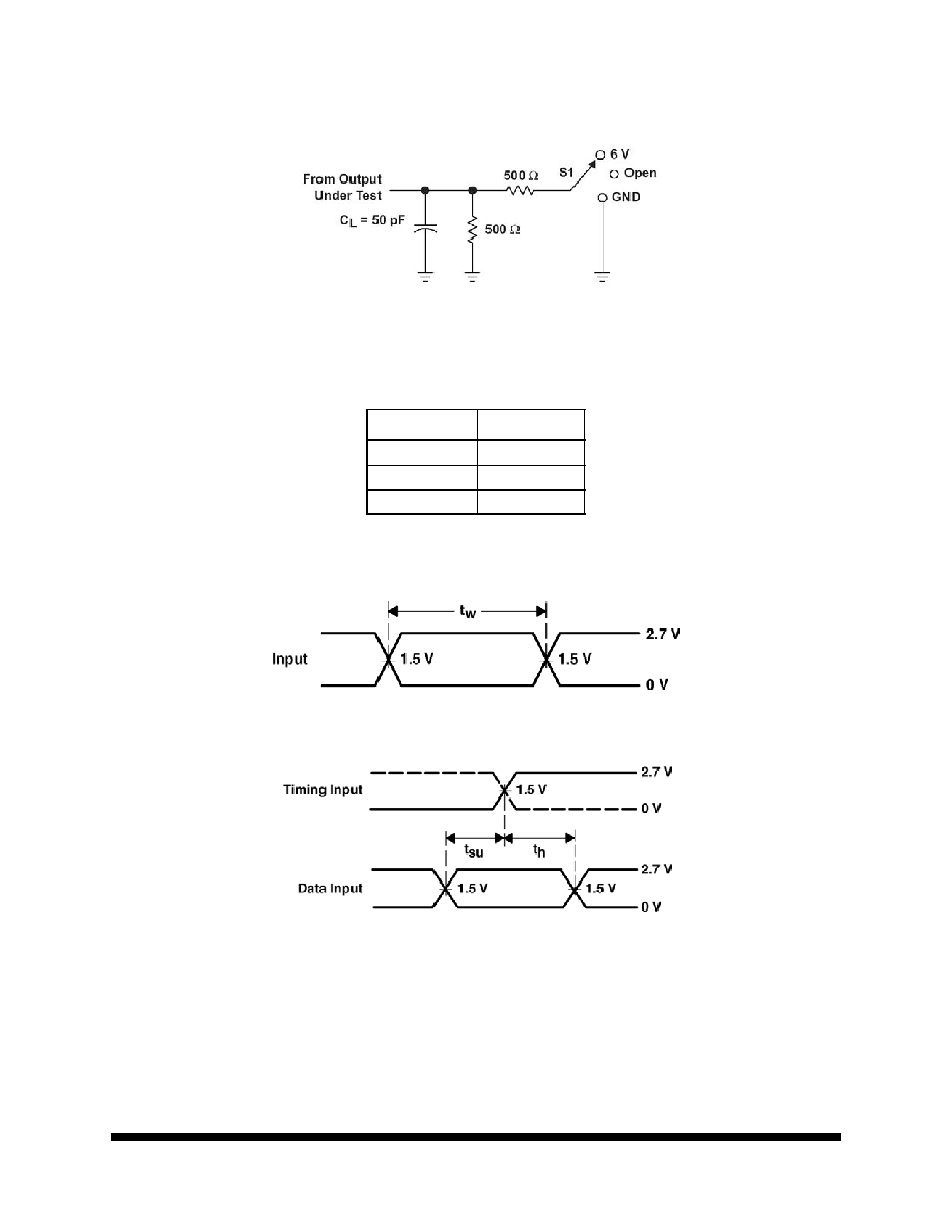
F
IGURE
1. L
OAD
C
IRCUIT
Figure Note:
1. C
L
includes probe and jig capacitance.
F
IGURE
2. P
ULSE
D
URATION
F
IGURE
3. S
ETUP
AND
H
OLD
T
IMES
P
ARAMETER
M
EASUREMENT
I
NFORMATION
T
EST
S1
t
PLH
/t
PHL
Open
t
PLZ
/t
PZL
6V
t
PHZ
/t
PZH
GND