 | –≠–ª–µ–∫—Ç—Ä–æ–Ω–Ω—ã–π –∫–æ–º–ø–æ–Ω–µ–Ω—Ç: 7809LP | –°–∫–∞—á–∞—Ç—å:  PDF PDF  ZIP ZIP |


M
e
m
o
r
y
3
All data sheets are subject to change without notice
©2005 Maxwell Technologies
All rights reserved.
16-Bit Latchup Protected Analog to Digital Converter
7809LP
01.11.05 Rev 7
21
BUSY
Busy Output. Falls when a conversion is started, and remains LOW until the conversion is com-
pleted and the data is latched into the output shift register. CS or R/C must be HIGH when
BUSY rises, or another conversion will start without time for signal acquisition.
22
PWRD
Power Down Input. If HIGH, conversions are inhibited and power consumption is significantly
reduced. Results from the previous conversions are maintained in the output shift register.
23
LPVANA
Latchup Protection Analog Supply.
24
LPVDIG
Latchup Protection Digital Supply.
T
ABLE
2. 7809LP A
BSOLUTE
M
AXIMUM
R
ATINGS
P
ARAMETER
S
YMBOL
M
IN
M
AX
U
NIT
Analog Inputs
R1
IN
R2
IN
R3
IN
CAP
REF
1
1. Indefinite short to AGND2, momentarily short to V
ANA
.
-25
-25
-25
V
ANA
+ 0.3
25
25
25
AGND2 - 0.3
V
V
V
V
Ground Voltage Differences: DGND, AGND2
-0.3
0.3
V
V
ANA
--
7
V
V
DIG
7
V
V
DIG
to V
ANA
--
0.3
V
Specified Performance
-40
85
∞
C
Digital Inputs
-0.3
V
DIG
+ 0.3
V
Storage Temperature
T
STG
-65
150
∞
C
T
ABLE
3. 7809LP DC A
CCURACY
S
PECIFICATIONS
(S
PECIFIED
P
ERFORMANCE
-40
TO
+85∞C)
P
ARAMETER
M
IN
T
YP
M
AX
U
NIT
Integral Linearity Error
-40 to 85∞C
--
--
--
--
±3
±5
LSB
1
Differential Linearity Error
-40 to 85∞C
--
--
--
--
-2, 3
-1, 6
LSB
LSB
No Missing Codes
2
15
--
--
Bits
Transition Noise
3
--
1.3
--
LSB
Full Scale Error
4,5
--
--
±0.6
%
Full Scale Error
4,5
(using ext. 2.5000 V
ref
)
--
±0.6
%
Full Scale Error Drift
--
±7
--
ppm/
∞
C
T
ABLE
1. 7809LP P
IN
D
ESCRIPTION
P
IN
S
YMBOL
D
ESCRIPTION

M
e
m
o
r
y
4
All data sheets are subject to change without notice
©2005 Maxwell Technologies
All rights reserved.
16-Bit Latchup Protected Analog to Digital Converter
7809LP
01.11.05 Rev 7
Full Scale Error Drift (using ext. 2.5000 V
ref
)
--
±2
--
ppm/
∞
C
Bipolar Zero Error
4
--
--
±10
mV
Bipolar Zero Error Drift
--
±2
--
ppm/
∞
C
Unipolar Zero Error
4
-40 to 85∞C
--
--
--
--
±3
±16
mV
mV
Unipolar Zero Error Drift
--
±2
--
ppm/
∞
C
Recovery to Rated Accuracy after Power Down (1 uF Capacitor to
CAP)
--
1
--
ms
Power Supply Sensitivity (V
DIG
= V
ANA
= V
D
) 4.75 V > V
D
< 5.2 V
-40 to 85∞C
--
--
--
--
±8
±32
LSB
LSB
1. LSB stands for Least Significant Bit. One LSB is equal to 305 µ V.
2. Not tested.
3. Typical rms noise at worst case transitions and temperatures.
4. Measured with various fixed resistors.
5. For bipolar input ranges, full scale error is the worst case of -Full Scale or +Full Scale untrimmed deviation from ideal first and
last scale code transitions, divided by the transition voltage (not divided by the full-scale range) and includes the effect of offset
error. For unipolar input ranges, full scale error is the deviation of the last code transition divided by the transition voltage. It
also includes the effect of offset error.
T
ABLE
4. D
ELTA
L
IMITS
P
ARAMETER
V
ARIATION
I
CC
+/- 10%
T
ABLE
5. 7809LP D
IGITAL
I
NPUTS
(S
PECIFIED
P
ERFORMANCE
-40
TO
+85∞C)
P
ARAMETER
S
UBGROUPS
M
IN
T
YP
M
AX
U
NIT
V
IL
V
IH
I
IL
, I
IH
1, 2, 3
-0.3
2.0
--
--
--
--
0.8
V
D
+ 0.3
±10
V
V
µ A
T
ABLE
3. 7809LP DC A
CCURACY
S
PECIFICATIONS
(S
PECIFIED
P
ERFORMANCE
-40
TO
+85∞C)
P
ARAMETER
M
IN
T
YP
M
AX
U
NIT

M
e
m
o
r
y
5
All data sheets are subject to change without notice
©2005 Maxwell Technologies
All rights reserved.
16-Bit Latchup Protected Analog to Digital Converter
7809LP
01.11.05 Rev 7
T
ABLE
6. 7809LP A
NALOG
I
NPUT
AND
T
HROUGHPUT
S
PEED
(S
PECIFIED
P
ERFORMANCE
-40
TO
+85∞C)
P
ARAMETER
S
UBGROUPS
M
IN
T
YP
M
AX
U
NIT
Voltage Ranges
10 V, 0 V to 5 V
See Table 2.
Impedance
Capacitance
1
1. Guarenteed by design.
1, 2, 3
--
35
--
pF
Conversion Time
9, 10, 11
--
7.6
8
µ s
Complete Cycle (Acquire and Convert)
9, 10, 11
--
--
10
µ s
Throughput Rate
2
2. Tested by application of signal.
9, 10, 11
100
--
--
kHz
T
ABLE
7. 7809LP AC A
CCURACY
S
PECIFICATIONS
(S
PECIFIED
P
ERFORMANCE
-40
TO
+85∞C)
P
ARAMETER
S
UBGROUPS
M
IN
T
YP
M
AX
U
NIT
Spurious-Free Dynamic Range, f
IN
= 20 kHz
1
1. Guaranteed by design.
4, 5, 6
90
100
--
dB
2
2. All specifications in dB are referred to a full-scale ±10 V input.
Total Harmonic Distortion, f
IN
= 20 kHz
1
4, 5, 6
--
-100
-90
dB
Signal-to-Noise (Noise + Distortion)
1
f
IN
= 20 kHz
-60 dB Input
4, 5, 6
83
--
88
30
--
--
dB
Signal-to-Noise
1
, f
IN
= 20 kHz
83
88
--
dB
Full-Power Bandwidth
1,3
3. Full-Power Bandwidth defined as Full-Scale input frequency at which Signal-to-Noise (Noise + Distortion) degrades to 60 dB.
9, 10, 11
--
250
--
kHz
T
ABLE
8. 7809LP S
AMPLING
D
YNAMICS
(S
PECIFIED
P
ERFORMANCE
-40
TO
+85∞C)
P
ARAMETER
S
UBGROUPS
M
IN
T
YP
M
AX
U
NIT
Aperture Delay
9, 10, 11
--
40
--
ns
Aperture Jitter
9, 10, 11
Sufficient to meet AC specification
Transient Response FS Step
9, 10, 11
--
2
--
us
Overvoltage Recovery
1
1. Recovers to specified performance after 2 X FS input overvoltage.
9, 10, 11
--
150
--
ns

M
e
m
o
r
y
6
All data sheets are subject to change without notice
©2005 Maxwell Technologies
All rights reserved.
16-Bit Latchup Protected Analog to Digital Converter
7809LP
01.11.05 Rev 7
T
ABLE
9. 7809LP R
EFERENCE
(S
PECIFIED
P
ERFORMANCE
-40
TO
+85∞C)
P
ARAMETER
C
ONDITIONS
M
IN
T
YP
M
AX
U
NIT
Internal Reference Voltage
No Load
2.48
2.5
2.52
V
Internal Reference Source Current (Must be
ext. buffer)
--
1
--
µ A
External Reference Voltage Range for Speci-
fied Linearity
1
1. Tested by application of signal.
2.3
2.5
2.7
V
External Reference Current Drain
Ext. 2.5000V Ref
--
--
100
µ A
T
ABLE
10. 7809LP D
IGITAL
O
UTPUTS
(S
PECIFIED
P
ERFORMANCE
-40
TO
+85∞C)
P
ARAMETER
S
UBGROUPS
C
ONDITIONS
M
IN
T
YP
M
AX
U
NIT
Data Format
Data Coding
Pipeline Delay
Serial 16-bits
Binary Two's Complement or Straight Binary
Conversion results only available after completed conversion
Data Clock
Internal (Output Only When
Transmitting Data)
External (Can Run Continually)
Selectable for internal or external data clock
9, 10, 11
EXT/INT Low
EXT/INT High
--
0.1
2.3
--
--
10
MHz
V
OL
V
OH
1, 2, 3
I
SINK
= 1.6 mA
I
SOURCE
= 500 µ A
--
4
--
--
0.4
--
V
Leakage Current
1
1. Not tested.
1, 2, 3
High-Z State,
V
OUT
= 0V to V
DIG
--
--
±10
µ A
Output Capacitance
1
1, 2, 3
High-Z State
--
15
--
pF
T
ABLE
11. 7809LP P
OWER
S
UPPLIES
(S
PECIFIED
P
ERFORMANCE
-40
TO
+85∞C)
P
ARAMETER
S
UBGROUPS
C
ONDITIONS
M
IN
T
YP
M
AX
U
NIT
V
DIG
1, 2, 3
Must be < V
ANA
4.75
5
5.25
V
V
ANA
1, 2, 3
4.75
5
5.25
V
I
DIG
1, 2, 3
--
0.3
--
mA
I
ANA
1, 2, 3
--
16
--
mA
Power Dissipation
PWRD LOW
PWRD HIGH
1, 2, 3
V
ANA
= V
DIG
= 5V
f
s
= 100 kHz
--
--
--
--
132
100
mW

M
e
m
o
r
y
7
All data sheets are subject to change without notice
©2005 Maxwell Technologies
All rights reserved.
16-Bit Latchup Protected Analog to Digital Converter
7809LP
01.11.05 Rev 7
T
ABLE
12. 7809LP C
ONTROL
L
INE
F
UNCTIONS
FOR
R
EAD
AND
C
ONVERT
S
PECIFIC
F
UNCTION
CS
R/C
BUSY
EXT/INT
DATACL
K
PWRD
SB/BTC
O
PERATION
Initiate Conver-
sion and Output
Data using Inter-
nal Clock
1 > 0
0
0
1 > 0
1
1
0
0
Output
Output
0
0
x
x
Initiates conversion "n".
Data from conversion "n-
1" clocked out on DATA
synchronized to 16 clock
pulses output on DATA-
CLK
Initiates conversion "n".
Data from conversion "n-
1" clocked out on DATA
synchronized to 16 clock
pulses output on DATA-
CLK
Initiate Conver-
sion and Output
Data using Exter-
nal Clock
1 > 0
0
1 > 0
1 > 0
0
0
1 > 0
1
1
0 > 1
1
1
1
0
0
1
1
1
1
1
Input
Input
Input
Input
Input
0
0
x
0
0
x
x
x
x
x
Initiates conversion "n"
Initiates conversion "n"
Outputs a pulse on SYNC
followed by data from con-
version "n" clocked out
synchronized to external
DATACLK.
Outputs a pules on SYNC
followed by data from con-
version "n-1" clocked out
synchronized to external
DATACLK
1
. Conversion
"n" in process.
Outputs a pulse on SYNC
followed by data from con-
version "n-1" clocked out
synchronized to external
DATACLK
1
. Conversion
"n" in process.
Incorrect Conver-
sions
0
0
0 > 1
x
x
0
x
CS or R/C must be HIGH
or a new conversion will
be initiated without time
for acquisition
Power Down
x
x
x
x
x
x
x
x
x
x
0
1
x
x
Analog circuitry powered.
Conversion will be initi-
ated without time for
acquisition
Analog circuitry disabled.
Data from previous con-
version maintained in out-
put registers

M
e
m
o
r
y
8
All data sheets are subject to change without notice
©2005 Maxwell Technologies
All rights reserved.
16-Bit Latchup Protected Analog to Digital Converter
7809LP
01.11.05 Rev 7
Selecting Output
Format
x
x
x
x
x
x
x
x
x
x
x
x
0
3
1
Serial data is output in
Binary Two's Comple-
ment format.
Serial data is output in
Straight Binary format.
1. See Figure 4 for constraints on previous data valid during conversion.
T
ABLE
13. 7809LP I
NPUT
R
ANGE
C
ONNECTION
A
NALOG
I
NPUT
R
ANGE
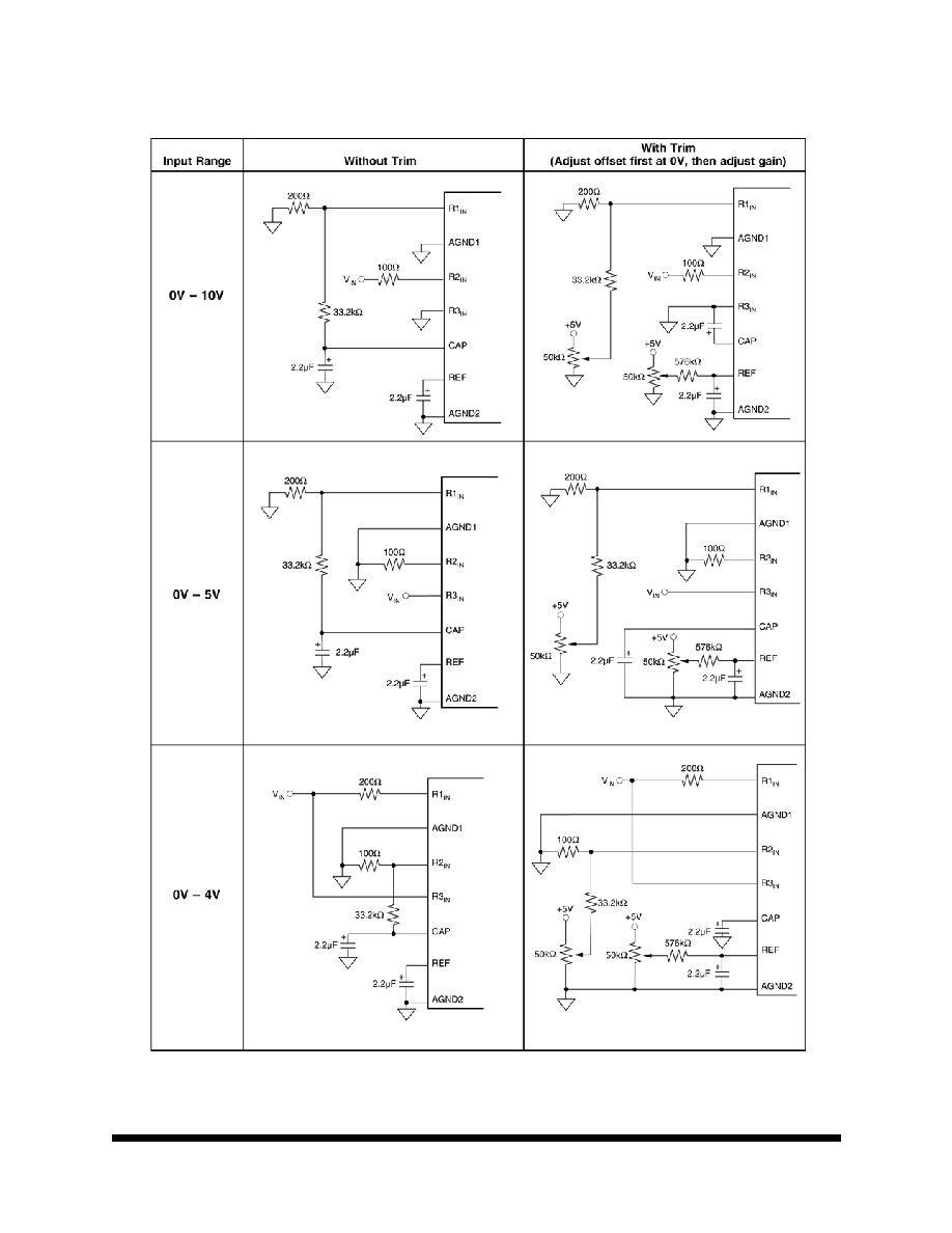
C
ONNECT
R1
IN
VIA
200
TO
C
ONNECT
R2
IN
VIA
100
TO
C
ONNECT
R3
IN
TO
I
MPEDANCE
±10V
V
IN
AGND
CAP
22.9 k
±5V
AGND
V
IN
CAP
13.3 k
±3.3V
V
IN
V
IN
CAP
10.7 k
0V to 10V
AGND
V
IN
AGND
13.3k
0V to 5V
AGND
AGND
V
IN
10.0 k
0V to 4V
V
IN
AGND
V
IN
10.7 k
T
ABLE
14. 7809LP C
ONVERSION
AND
D
ATA
T
IMING
(T
A
= -40
∞
C
TO
85
∞
C
UNLESS
OTHERWISE
SPECIFIED
)
S
YMBOL
D
ESCRIPTION
S
UBGROUPS
M
IN
T
YP
M
AX
U
NIT
t1
Convert Pulse Width
9, 10, 11
40
--
6000
ns
t2
BUSY Delay
9, 10, 11
--
--
65
ns
t3
BUSY LOW
9, 10, 11
--
--
8
µ s
t4
BUSY Delay after End of Conversion
9, 10, 11
--
220
--
ns
t5
Aperture Delay
9, 10, 11
--
40
--
ns
t6
Conversion Time
9, 10, 11
--
7.6
8
µ s
t7
Acquisition Time
9, 10, 11
--
--
2
µ s
t6 + t7
Throughput Time
9, 10, 11
--
9
10
µ s
t8
R/C Low to DATACLK Delay
9, 10, 11
--
450
--
ns
t9
DATACLK Period
9, 10, 11
--
440
--
ns
t10
Data Valid to DATACLK HIGH Delay
9, 10, 11
20
75
--
ns
t11
Data Valid after DATACLK LOW
Delay
9, 10, 11
100
125
--
ns
t12
External DATACLK
9, 10, 11
100
--
--
ns
T
ABLE
12. 7809LP C
ONTROL
L
INE
F
UNCTIONS
FOR
R
EAD
AND
C
ONVERT
S
PECIFIC
F
UNCTION
CS
R/C
BUSY
EXT/INT
DATACL
K
PWRD
SB/BTC
O
PERATION

M
e
m
o
r
y
9
All data sheets are subject to change without notice
©2005 Maxwell Technologies
All rights reserved.
16-Bit Latchup Protected Analog to Digital Converter
7809LP
01.11.05 Rev 7
t13
External DATACLK HIGH
9, 10, 11
20
--
--
ns
t14
External DATACLK LOW
9, 10, 11
30
--
--
ns
t15
DATACLK HIGH Setup Time
9, 10, 11
20
--
t12 + 5
ns
t16
R/C to CS Setup Time
9, 10, 11
10
--
--
ns
t17
SYNC Delay After DATACLK High
9, 10, 11
15
--
35
ns
t18
Data Valid Delay
9, 10, 11
25
--
55
ns
t19
CS to Rising Edge Delay
9, 10, 11
25
--
--
ns
t20
Data Available after CS LOW
9, 10, 11
6
--
--
µ s
T
ABLE
15. 7809LP C
ONVERSION
D
ATA
T
IMING
D
ESCRIPTION
A
NALOG
I
NPUT
D
IGITAL
O
UTPUT
B
INARY
T
WO
'
S
C
OMPLEMENT
(SB/BTC
LOW)
S
TRAIGHT
B
INARY
(SB/BTC H
IGH
)
B
INARY
C
ODE
H
EX
C
ODE
B
INARY
C
ODE
H
EX
C
ODE
Full Scale
Range
±10
±5
±3.33V
0V to
10V
0V to 5V 0V to 4V
Least Signifi-
cant Bit (LSB)
305 µ V
153 µ V
102 µ V
153 µ V
76 µ V
61 µ V
+ Full Scale
(FS - 1 LSB)
9.99969
5V
4.99984
7V
3.33323
1V
9.99984
7V
4.99992
4V
3.99993
8V
0111 1111
1111 1111
7FFF
1111 1111
1111 1111
FFFF
Midscale
0V
0V
0V
5V
2.5V
2V
0000 0000
0000 0000
0000
1000 0000
0000 0000
8000
One LSB
Below Mid-
scale
-305 µ V -153 µ V -102 µ V
4.99984
7V
2.49992
4V
1.99993
9V
1111 1111
1111 1111
FFFF
0111 1111
1111 1111
7FFF
-Full Scale
-10V
-5V
3.33333
3V
0V
0V
0V
1000 0000
0000 0000
8000
0000 0000
0000 0000
0000
T
ABLE
14. 7809LP C
ONVERSION
AND
D
ATA
T
IMING
(T
A
= -40
∞
C
TO
85
∞
C
UNLESS
OTHERWISE
SPECIFIED
)
S
YMBOL
D
ESCRIPTION
S
UBGROUPS
M
IN
T
YP
M
AX
U
NIT

M
e
m
o
r
y
10
All data sheets are subject to change without notice
©2005 Maxwell Technologies
All rights reserved.
16-Bit Latchup Protected Analog to Digital Converter
7809LP
01.11.05 Rev 7
F
IGURE
1. C
ONVERSION
T
IMING
F
IGURE
2. S
ERIAL
D
ATA
T
IMING
U
SING
I
NTERNAL
C
LOCK
(CS, EXT/INT
AND
TAG
TIED
LOW)
F
IGURE
3. C
ONVERSION
AND
R
EAD
T
IMING
WITH
E
XTERNAL
C
LOCK
(EXT/INT
TIED
HIGH). R
EAD
A
FTER
C
ONVERSION
M
e
m
o
r
y
11
All data sheets are subject to change without notice
©2005 Maxwell Technologies
All rights reserved.
16-Bit Latchup Protected Analog to Digital Converter
7809LP
01.11.05 Rev 7
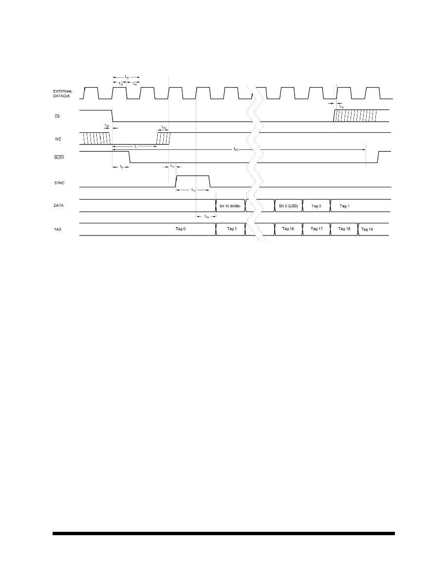
F
IGURE
4. C
ONVERSION
AND
R
EAD
T
IMING
WITH
E
XTERNAL
C
LOCK
(EXT/INT
TIED
HIGH). R
EAD
D
URING
C
ONVERSION
M
e
m
o
r
y
12
All data sheets are subject to change without notice
©2005 Maxwell Technologies
All rights reserved.
16-Bit Latchup Protected Analog to Digital Converter
7809LP
01.11.05 Rev 7
F
IGURE
5. O
FFSET
/G
AIN
C
IRCUITS
FOR
U
NIPOLAR
I
NPUT
R
ANGES
M
e
m
o
r
y
13
All data sheets are subject to change without notice
©2005 Maxwell Technologies
All rights reserved.
16-Bit Latchup Protected Analog to Digital Converter
7809LP
01.11.05 Rev 7
F
IGURE
6. O
FFSET
/G
AIN
C
IRCUITS
FOR
B
IPOLAR
I
NPUT
R
ANGES
M
e
m
o
r
y
14
All data sheets are subject to change without notice
©2005 Maxwell Technologies
All rights reserved.
16-Bit Latchup Protected Analog to Digital Converter
7809LP
01.11.05 Rev 7
LPT
TM
Operation
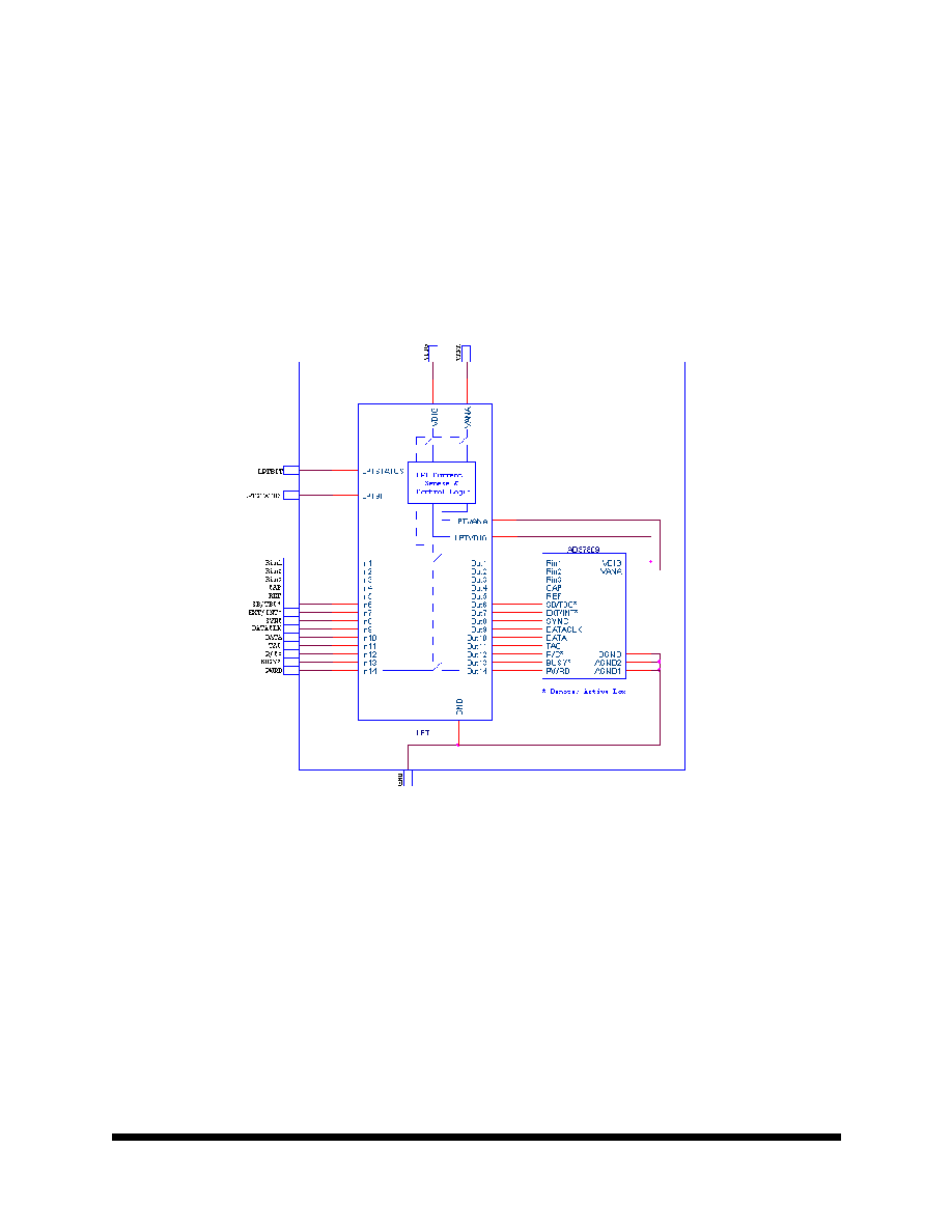
Latchup Protection Technology (LPT
TM
) automatically detects an increase in the supply current of the 7809LP con-
verter due to a single event effect and internally cycles the power to the converter off, then on, which restores the
steady state operation of the device. A simplified block diagram of the 7809LP circuitry is shown in Figure 7. The
LPT
TM
circuitry consists of two power switch and current sensor blocks, an LPT
TM
controller block, a BIT current load
block, and an active input protection block.
Figure 7. 7809LP Simplified Block Diagram
The power switch/current sensor blocks sense the supply current drawn by the protected device on the analog and
digital supply pins. When a threshold level is exceeded on either supply line, indicating single event induced latchup of
the protected device, a signal is sent to the LPT
TM
controller block. The LPT
TM
controller then drives the power
switches to an off state which removes the power supplies from the protected device. At the same time, a signal is
sent to open the active input protection circuits and the LPSTATUS output pin is activated. After a period of time suffi-
cient to clear the latchup, the LPT
TM
controller drives the power switches and input protection back to the on state
restoring the operation of the protected device. The LPTBIT circuit is used during system test to electrically trigger the
latchup function by drawing current through the power switch/current sensor blocks sufficient to trigger the LPT
TM
pro-
tection.

M
e
m
o
r
y
15
All data sheets are subject to change without notice
©2005 Maxwell Technologies
All rights reserved.
16-Bit Latchup Protected Analog to Digital Converter
7809LP
01.11.05 Rev 7
Differences Between the 7809LP and the ADS7809
Because the 7809LP uses the ADS7809 die to perform the analog to digital conversion function, its operation and per-
formance is very similar to the ADS7809 packaged part from Burr-Brown. In general the operation and application will
be the same for both parts. There are three primary differences: the operation of the supply pins, the operation of the
additional LPBIT and LPSTATUS pins, and the operation of the I/O pins when a latchup is detected.
The ADS7809 provides separate analog and digital supply pins, VANA and VDIG. These same supply pins on the
7809LPRP should be connected to the analog and digital supplies. There is no limit to the capacitance that can be
connected to these pins in the system application.
The 7809LP package also provides access to the ADS7809 die supply pins with the LPVANA and LPVDIG pins. The
signal paths between the supply input pins and the respective die supply pins are low resistance during normal device
operation. When an excessive supply current due to a single event latchup is sensed on either of the supply pins, the
LPT
TM
circuit opens both paths to the die supply pins allowing the latchup condition to clear. The LPVANA and LPV-
DIG pins allow access to the current sense circuitry for electrical testing at the component level and provide optimal
locations for attaching supply decoupling capacitors. CAUTION: The LPVANA and LPVDIG pins must not be con-
nected to the respective power supplies since this will defeat the LPT
TM
power switch and could result in permanent
latchup of the device during operation in a radiation environment. Electrolytic capacitors should not be connected to
these decoupling pins because the large capacitance will increase the recovery time of the 7809LP. Low ESR ceramic
capacitors should be used with a maximum of .2µ F per pin.
The LPBIT input provides a means to electrically test the LPT
TM
circuit. A high level on the this pin causes a preset
current to be drawn in addition to the normal device current through the analog and digital current sensors. If the high
level is maintained for a sufficient duration, it will trigger the LPT
TM
circuit which will cycle the power to the protected
device. If the LPBIT remains high, the LPT
TM
circuit will continuously cycle the supply voltages off then on. Driving this
input with a 10 µ s high level pulse is sufficient duration to assure the LPT
TM
circuit cycles the power off then on one
time only.
A high level on the LPSTATUS output indicates that the LPT
TM
circuit has removed power from the protected device.
The LPSTATUS returns low when the power is restored. LPSTATUS can be used to generate an input to the system
data processor indicating that an LPT
TM
cycle has occurred and the protected device output accuracy may not be met
until after the respective recovery time to the event.
During the time that power is removed from the protected device, it is critical that external circuitry driving the device I/
O pins does not back-drive the device supply through input protection diodes or similar integrated structures. Back-
driving of the supply through the device I/O pins could contribute to an extended or even a permanent latchup condi-
tion. For the ADS7809 testing has shown that for the normal signal range of operation on the analog input pins R1IN,
R2IN, and R3IN, latchup will not be sustained.
In order to prevent back-driving the supply from the digital I/O pins DATA, SYNC, TAG, R/C, CS, and PWRD, the
7809LP incorporates active input protection circuits. These circuits act as transmission gates in series with the digital
inputs. During normal operation, these gates are on and present low resistance connections between the package
input pins and the respective die pins. When the LPT
TM
circuit detects a latchup, these gates are switched off and
present a high resistance path between the package inputs and the die inputs. The protected I/O pins are crow barred
during the latchup. The bidirectional signal, DATACLK, is also protected by a transmission gate.

M
e
m
o
r
y
16
All data sheets are subject to change without notice
©2005 Maxwell Technologies
All rights reserved.
16-Bit Latchup Protected Analog to Digital Converter
7809LP
01.11.05 Rev 7
Dedicated digital outputs are not similarly protected since in most applications there will be no appreciable drive signal
on these outputs to back-drive the pins. Pull up resistors on these outputs should be 10 K
or greater to limit the
back-drive current. Low on resistance, transmission gate circuits are also connected between the package pins and
the die REF and CAP pins. These gates minimize the transient loading on the external filter capacitors required on
these pins. This greatly reduces the single event recovery time of the 7809LP to full accuracy after an LPT
TM
cycle.
During an LPT
TM
cycle, all outputs of the 7809LP are invalid and unpredictable until after the functional recovery time.
After the functional recovery time, data conversions occur with a degraded accuracy until the full accuracy recovery
time.
A summary of the pin differences between the ADS7809 and the 7809LP is provided in the table below.
T
ABLE
15. ADS7809
AND
7809LP P
IN
D
IFFERENCES
P
IN
N
UMBER
ADS7809
7809LPRP
P
IN
D
IFFERENCE
D
ESCRIPTION
1-10
Various
Various
Equivalent function to ADS7809 pins 1-10 respectively. Timing specifications
change slightly (0 - 10 ns) for the 7809LPRP due to the latchup protection circuitry
on ADS7809 die inputs.
15-22
Various
Various
Equivalent function to ADS7809 pins 11-18 respectively. Timing specifications
change slightly (0 - 10 ns) for the 7809LPRP due to the latchup protection circuitry
on ADS7809 die inputs.
11
--
LPBIT
A built in test function of latchup protection. A TTL high level pulse for > 5 microsec-
onds duration on this input will trigger latchup protection of the device. This input
shall be low during normal operation.
12
--
LPSTATUS
Latchup protection status output. This TTL level output is low during normal opera-
tion and goes high during a 10 µ s decision time period prior to power being
removed. If the latch up current does not last at least 10 µ s then LPTSTATUS will
go low (inactive) after the 10 µ s decision period without power being removed.
When latchup protection is triggered, this output will go high for the duration of the
time that power is removed from the protected device (50 µ s). All output except
LPSTATUS are invalid during the time that power is removed from the ADS7809
die. This output foes low within 1 us of the power being re-applied to the protected
device. Functional operation of the device is within ~25 µ s after the LPSTATUS
output returns low with degraded accuracy due to the latchup filter circuitry. Full
accuracy is restored ~5 ms later. This output can be used to inform the system pro-
cessor of the latchup protection trigger and the subsequent degraded accuracy in
the 7809LPRP output data. Output pull-up resistors should be 10k
or larger on
outputs. I/O pins must not be driven high while this signal is active.
13
VANA
VANA
Equivalent function to ADS7809 pin 19. Analog Supply Input.
14
VDIG
VDIG
Equivalent function to ADS7809 pin 20. Digital Supply Input.
23
--
LPVANA
Latchup protected analog supply pin to the ADS7809 die. Decouple to analog
ground with 0.1 µ F ceramic capacitor. Do not exceed 0.2 µ F. Do not connect to
VDIG and/or VANA.
24
--
LPVDIG
Latchup protected digital supply pin to the ADS7809 die. Decouple to digital ground
with 0.1 µ F ceramic capacitor. Do not exceed 0.2 µ F. Do not connect to VDIG and/
or VANA.

M
e
m
o
r
y
17
All data sheets are subject to change without notice
©2005 Maxwell Technologies
All rights reserved.
16-Bit Latchup Protected Analog to Digital Converter
7809LP
01.11.05 Rev 7
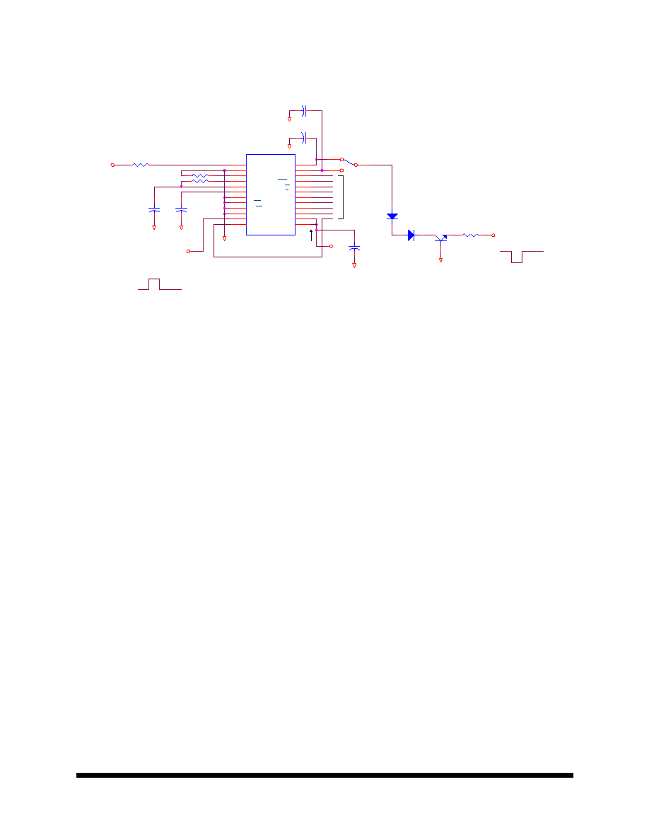
Testing the 7809LPRP Latchup Protection Circuitry
The LPVANA and LPVDIG pins provide direct access to the 7809LP converter supply pins for attaching external
decoupling capacitors to ground. These pins can also be used to test the LPT
TM
operation and threshold level by sink-
ing a pulsed current load to ground as shown in the test circuit in Figure 8. The most accurate threshold current mea-
surements are made with the ADS7809 in its lowest power state (PWRD = 5V).
The LPT
TM
operation and device recovery times are most easily measured using the LPBIT input to trigger protection
and recovery. Applying a 10 µ sec high duration TTL level to the LPBIT pin causes internal test currents sufficient to
trigger the LPT
TM
circuit to be drawn through both the analog and digital supply sense circuits.
LPT
TM
operating characteristics are summarized in Table 16 according to the timing diagram shown in Figure 9. Dur-
ing the time that the power is cycled, output signals and data from the 7809LP are invalid. The LPSTATUS signal high
indicates that power is removed from the ADS7809 die. When this signal is low, power is applied to the ADS7809 die.
The LPSTATUS signal is used to measure the supply recovery time. The supply recovery time interval starts when the
supply current rises (causing LPSTATUS to go high) and ends when the LPSTATUS signal stabilizes low again.
Within the functional recovery time interval (~25 µ sec after the LPT
TM
circuit reapplies power), the normal functional
operation of the converter is restored with less than 5% full scale error. Additional settling time is then required to
return to full accuracy operation. Recovery time intervals are defined which indicate the time to recover first to within 8
bit accuracy, then to within 12 bit accuracy, and finally to full 16 bit accuracy. These recovery times are primarily due to
the single event and power cycling effects on the reference circuits and the settling times of their respective filter
capacitors.
T
ABLE
16. 7809LP LPT
TM
O
PERATING
C
HARACTERISTICS
P
ARAMETER
S
YMBOL
C
ONDITIONS
T
YP
U
NIT
Supply Threshold Current
ITHR
PWRD = 5V
75
mA
Protection Time
TPT
LPBIT = 2.4V for 5 µ s
10
µ sec
Supply Recovery Time
TSR
LPBIT = 2.4V for 5 µ s
50
µ sec
Functional Recovery Time
TFR
LPBIT = 2.4V for 5 µ s
TSR + 25
µ sec
8-bit Accuracy Recovery Time
T8R
LPBIT = 2.4V for 5 µ s
80
µ sec
Full Accuracy Recovery Time
TFAR
LPBIT = 2.4V for 5 µ s
5
msec
M
e
m
o
r
y
18
All data sheets are subject to change without notice
©2005 Maxwell Technologies
All rights reserved.
16-Bit Latchup Protected Analog to Digital Converter
7809LP
01.11.05 Rev 7
F
IGURE
8. 7809LP LPT
TM
T
EST
C
IRCUIT
GND
PULSE GENERATOR 2
-7.5V
GND
GND
GND
GND
+5V
PULSE GENERATOR 1
GND
GND
0V
20 USEC PULSEWIDTH
-VP
IS
DIGITAL
CONTROL
AND
MONITORING
.4V
2.4V
5 USEC PULSEWIDTH
RT/FT < 10 NS
Q1
2N2369A
D2
1N4149
D1
1N4149
R3
50
R1
200
R2
100
R3
22.9K
C1
2.2UF
+
C2
2.2UF
+
U?
7809LPRP
R1IN
1
AGND1
2
R2IN
3
R3IN
4
CAP
5
REF
6
AGND2
7
SB/BTC
8
EXT/INT
9
DGND
10
LPBIT
11
LPSTATUS
12
VANA
13
VDIG
14
SYNC
15
DATACLK
16
DATA
17
TAG
18
R/C
19
CS
20
BUSY
21
PWRD
22
LPVANA
23
LPVDIG
24
C3
10UF
+
S1
C4
.1UF
C4
.1UF

M
e
m
o
r
y
19
All data sheets are subject to change without notice
©2005 Maxwell Technologies
All rights reserved.
16-Bit Latchup Protected Analog to Digital Converter
7809LP
01.11.05 Rev 7
F
IGURE
9. 7809LP LPT
TM
T
IMING
D
IAGRAM
SUPPLY CURRENT (IS)
IS (TYP)
0V
OUTPUTS
VALID
ITHR
TFAR
<1/4096 F.S.
TSR
-VP
FULL
ACCURACY
FULL SCALE (F.S.)
LPSTATUS
CHARGE CURRENT INTO
0V
- FULL SCALE
ALL OUTPUTS
IS PEAK
TFR
0
IS (TYP)
OUTPUTS
T12R
>-1/20 F.S.
PULSE GENERATOR 2
<1/256 F.S.
OUTPUT DATA
ERROR
T8R
FULL
ACCURACY
<1/20 F.S.
DECOUPLING CAPACITOR
TPT
5V
PULSE GENERATOR 1
.4V
2.4V
LPBIT
INVALID
OUTPUTS
VALID

M
e
m
o
r
y
20
All data sheets are subject to change without notice
©2005 Maxwell Technologies
All rights reserved.
16-Bit Latchup Protected Analog to Digital Converter
7809LP
01.11.05 Rev 7
F
IGURE
10. SEL C
ROSS
S
ECTION
F
IGURE
11. SEU C
ROSS
S
ECTION
M
e
m
o
r
y
21
All data sheets are subject to change without notice
©2005 Maxwell Technologies
All rights reserved.
16-Bit Latchup Protected Analog to Digital Converter
7809LP
01.11.05 Rev 7
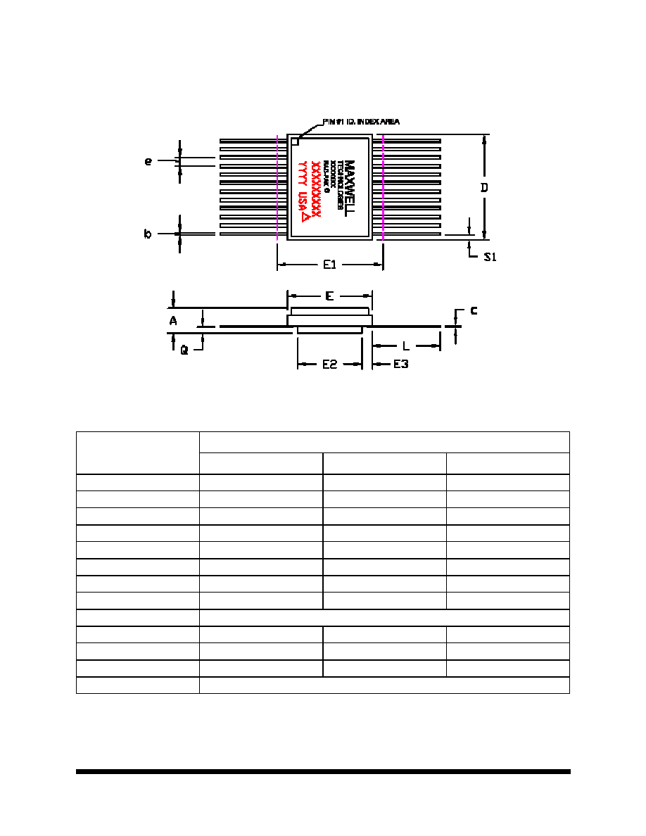
Note: All dimensions in inches
24-P
IN
R
AD
-P
AK
Æ F
LAT
P
ACKAGE
S
YMBOL
D
IMENSION
M
IN
N
OM
M
AX
A
0.255
0.278
0.302
b
0.015
0.017
0.022
c
0.006
0.008
0.010
D
--
0.596
0.640
E
0.900
0.400
0.410
E1
--
--
0.440
E2
0.268
0.270
0.272
E3
0.055
0.065
--
e
0.050 BSC
L
0.420
0.430
0.045
Q
0.040
0.045
0.006
S1
0.006
0.014
--
N
24

M
e
m
o
r
y
22
All data sheets are subject to change without notice
©2005 Maxwell Technologies
All rights reserved.
16-Bit Latchup Protected Analog to Digital Converter
7809LP
01.11.05 Rev 7
Important Notice:
These data sheets are created using the chip manufacturers published specifications. Maxwell Technologies verifies
functionality by testing key parameters either by 100% testing, sample testing or characterization.
The specifications presented within these data sheets represent the latest and most accurate information available to
date. However, these specifications are subject to change without notice and Maxwell Technologies assumes no
responsibility for the use of this information.
Maxwell Technologies' products are not authorized for use as critical components in life support devices or systems
without express written approval from Maxwell Technologies.
Any claim against Maxwell Technologies must be made within 90 days from the date of shipment from Maxwell Tech-
nologies. Maxwell Technologies' liability shall be limited to replacement of defective parts.

M
e
m
o
r
y
23
All data sheets are subject to change without notice
©2005 Maxwell Technologies
All rights reserved.
16-Bit Latchup Protected Analog to Digital Converter
7809LP
01.11.05 Rev 7
Product Ordering Options
Model Number
Feature
Option Details
7809LP
RP
F
X
Screening Flow
Package
Radiation Feature
Base Product
Nomenclature
Multi Chip Module (MCM)
1
K = Maxwell Self-Defined Class K
H = Maxwell Self-Defined Class H
I = Industrial (testing @ -40∞C,
+25∞C, +85∞C)
E = Engineering (testing @ +25∞C)
F = Flat Pack
RP = R
AD
-P
AK
Æ package
16-Bit Latchup Protected Analog
to Digital Converter
1) Products are manufactured and screened to Maxwell Technologies self-defined Class H and Class K flows.