
M
e
m
o
r
y
2
All data sheets are subject to change without notice
©2003 Maxwell Technologies
All rights reserved.
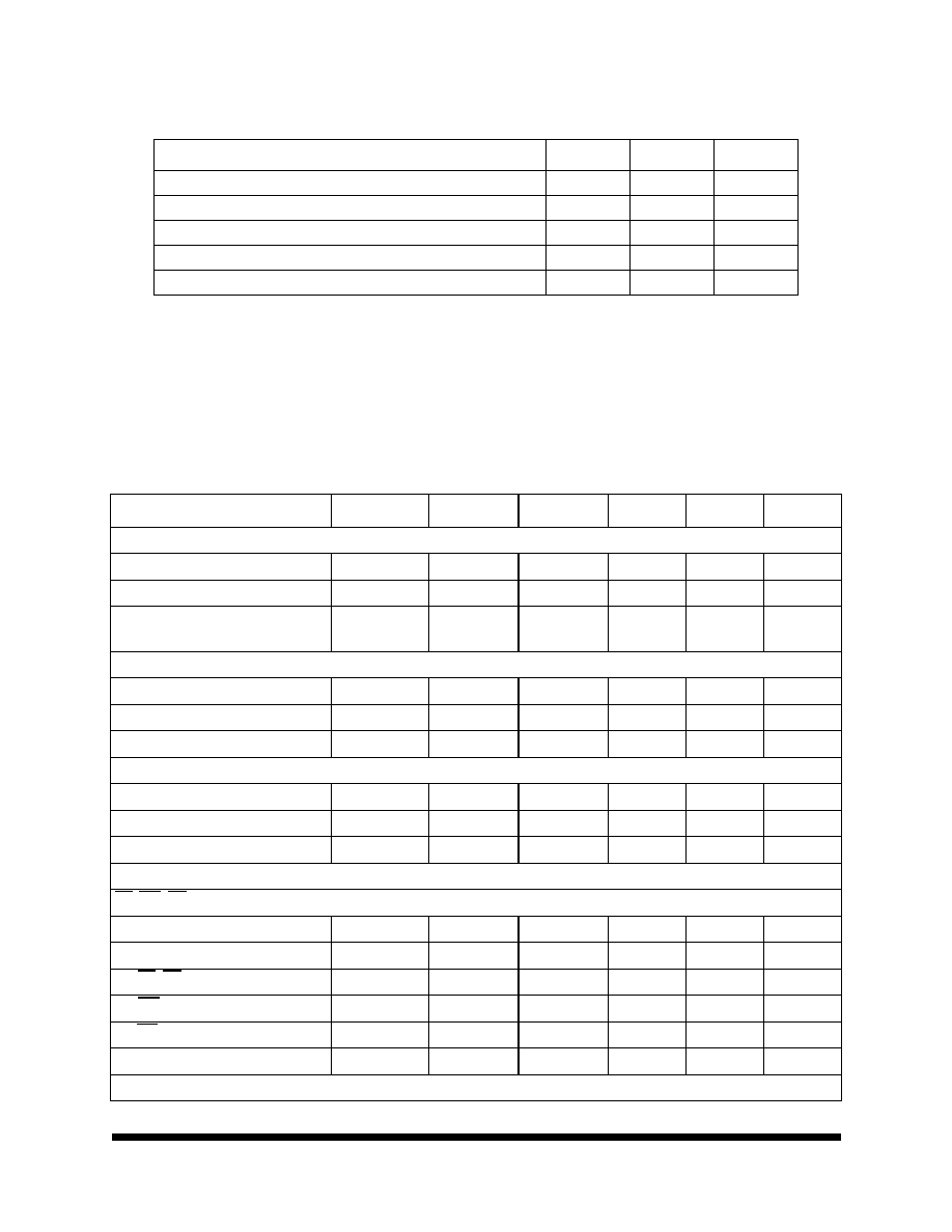
Microprocessor-compatible 8-Bit ADC
7820
09.09.03 Rev 3
T
ABLE
1. P
IN
D
ESCRIPTION
P
IN
S
YMBOL
D
ESCRIPTION
1
V
IN
Analog Input Range: V
REF(-)
to V
REF(+)
.
2
DB0
Data Output. Three State Output, bit 0 (LSB)
3
DB1
Data Output. Three State Output, bit 1
4
DB2
Data Output. Three State Output, bit 2
5
DB3
Data Output. Three State Output, bit 3
6
WR/RDY
WRITE control input/READY status output.
7
Mode
Mode Selection Input. It determines whether the device operates in the
WR-RD or RD mode. It is internally tied to GND through a 50 µ A current
source.
8
RD
READ Input. RD must be low to access data from the part.
9
INT
INTERUPT Output. INT going low indicates that the conversion is com-
plete INT returns high on rising the edge of RD or CS.
10
GND
Ground
11
V
REF-
Lower limit of reference span. Range: GND < V
REF(-)
< V
REF(+)
12
V
REF+
Upper limit of reference span. Range: GND < V
REF(-)
< V
REF(+)
< V
DD
13
CS
Chip Select Input. CS, the decoded device address, must be low for RD
or WR to be recognized by the converter.
14
DB4
Data Output. Three State Output, bit 4
15
DB5
Data Output. Three State Output, bit 5
16
DB6
Data Output. Three State Output, bit 6
17
DB7
Data Output. Three State Output, bit 7 (MSB)
18
OFL
Overflow Output. If the analog input is higher than (V
REF(+)
- 1/2LSB),
OFL will be low at the end of conversion. It is a non three state output
which can be used to cascade 2 or more devices to increase resolution.
19
NC
No Connection.
20
V
DD
Power supply voltage, +5V
T
ABLE
2. 7820 A
BSOLUTE
M
AXIMUM
R
ATINGS1
P
ARAMETER
M
IN
M
AX
U
NIT
V
DD
to GND
-0
7.0
V
Digital Input Voltage to GND (Pins 6-80, 13)
-0.3
V
DD
+0.3
V
Digital Output Voltage to GND (Pins 2-5, 9, 14-18)
0.3
V
DD
+0.3
V
V
REF
(+) to GND
0
V
DD
+0.3
V
V
REF
(-) to GND
V
SS
-0.3
V
REF
(+)
V
M
e
m
o
r
y
3
All data sheets are subject to change without notice
©2003 Maxwell Technologies
All rights reserved.
Microprocessor-compatible 8-Bit ADC
7820
09.09.03 Rev 3
V
IN
to GND
-0.3
V
DD
+0.3
V
Operating Temperature
-55
125
∞C
Storage Temperature Range
-65
150
∞C
Power Dissipation to 75∞C
--
450
mW
Derates above +75∞C
--
6
mW/∞C
1. CAUTION: ESD (electrostatic discharge) sensitive device. The digital control inputs are diode protected; how-
ever, permanent damage may occur on unconnected devices subject to high energy electrostatic fields. Unused
devices must be stored in conductive foam or shunts. The protective foam should be discharged to the destina-
tion socket before devices are inserted.
T
ABLE
3. 7820 DC E
LECTRICAL
C
HARACTERISTICS
(V
DD
= +5V; V
REF
(+) = +5V; V
REF
(-) = GND = 0V,
UNLESS
OTHERWISE
SPECIFIED
) (RD M
ODE
(P
IN
7 = 0V))
(T
A
= -55
TO
125 ∞C
UNLESS
OTHERWISE
SPECIFIED
)
P
ARAMETER
T
EST
C
ONDITIONS
S
UBGROUPS
M
IN
T
YP
M
AX
U
NIT
Accuracy
Resolution
--
8
--
--
Bits
Total Unadjusted Error
1
--
--
--
±1.0
LSB
Minimum Resolution for which No
Missing Codes are Guaranteed
--
--
--
8
Bits
Reference Input
Input Resisitance
--
1, 2, 3
1.0
--
4.0
k
V
REF
(+) Input Voltage Range
--
1, 2, 3
V
REF
(-)
--
V
DD
V
V
REF
(-) Input Voltage Range
--
1, 2, 3
GND
--
V
REF
(+)
V
Analog Input
Input Voltage Range
--
1, 2, 3
V
REF
(-)
--
V
REF
(+)
V
Input Leakage Current
--
1, 2, 3
--
--
±3
µ A
Input Capacitance
2
--
1, 2, 3
--
45
--
pF
Logic Inputs
CS, WR, RD
V
INH
--
1, 2, 3
2.4
--
--
V
V
INH
--
1, 2, 3
--
--
0.8
V
I
INH
(CS, RD)
--
1, 2, 3
--
--
1
µ A
I
INH
(WR)
--
1, 2, 3
--
--
3
µ A
I
INL
(WR)
--
1, 2, 3
--
--
-1
µ A
Input Capacitance
2
--
1, 2, 3
--
5
8
pF
T
ABLE
2. 7820 A
BSOLUTE
M
AXIMUM
R
ATINGS1
P
ARAMETER
M
IN
M
AX
U
NIT

M
e
m
o
r
y
4
All data sheets are subject to change without notice
©2003 Maxwell Technologies
All rights reserved.
Microprocessor-compatible 8-Bit ADC
7820
09.09.03 Rev 3
Mode
V
INH
--
1, 2, 3
3.5
--
--
V
I
INH
--
1, 2, 3
--
--
200
µ A
I
INL
--
1, 2, 3
--
--
-1
µ A
Input Capacitance
2
--
1, 2, 3
--
5
8
pF
Logic Outputs
DB0-DB7, OFL, INT
V
OH
ISOURCE =
360 µ A
1, 2, 3
4
--
--
V
V
OL
ISINK = 1.6 mA
1, 2, 3
--
--
0.4
V
I
OUT
(DB0-DB7)
Floating State
Leakage
1, 2, 3
--
--
±3
µ A
Output Capacitance
2
--
1, 2, 3
--
5
8
pF
RDY
V
OL
ISINK = 2.6mA
1, 2, 3
--
--
0.4
V
I
OUT
Floating State
Leakage
1, 2, 3
--
--
±3
V
Output Capacitance
2
--
4, 5, 6
--
5
8
pF
Slew Rate, Tracking
2
--
1, 2, 3
--
0.2
0.1
V/µ s
Power Supply
V
DD
±5% for speci-
fied perfor-
mance
1, 2, 3
--
--
5
V
I
DD
CS = RD = OV
1, 2, 3
--
--
20
mA
Power Dissipation
--
1, 2, 3
--
40
--
mW
Power Supply Sensitivity
VDD = 5V ±5%
1, 2, 3
--
±1/16
±1/4
LSB
1. Total unadjusted error includes offset, full scale and linearity error.
2. Guarenteed by design.
T
ABLE
3. 7820 DC E
LECTRICAL
C
HARACTERISTICS
(V
DD
= +5V; V
REF
(+) = +5V; V
REF
(-) = GND = 0V,
UNLESS
OTHERWISE
SPECIFIED
) (RD M
ODE
(P
IN
7 = 0V))
(T
A
= -55
TO
125 ∞C
UNLESS
OTHERWISE
SPECIFIED
)
P
ARAMETER
T
EST
C
ONDITIONS
S
UBGROUPS
M
IN
T
YP
M
AX
U
NIT

M
e
m
o
r
y
5
All data sheets are subject to change without notice
©2003 Maxwell Technologies
All rights reserved.
Microprocessor-compatible 8-Bit ADC
7820
09.09.03 Rev 3
T
ABLE
4. 7820 AC E
LECTRICAL
C
HARACTERISTICS1
(V
DD
= +5V; V
REF
(+) = +5V; V
REF
(-) = GND = 0V,
UNLESS
OTHERWISE
SPECIFIED
) (RD M
ODE
(P
IN
7 = 0V))
(T
A
= -55
TO
125 ∞C
UNLESS
OTHERWISE
SPECIFIED
)
1. Sample tested at 25∞C to ensure compliance. Only on process design change.
P
ARAMETER
S
UBGROUPS
S
YMBOL
M
IN
M
AX
U
NIT
CS to RD/WR Setup Time
9, 10, 11
t
CSS
0
--
ns
CS to RD/WR Hold Time
9, 10, 11
t
CSH
0
--
ns
CS to Delay Time (Pull-up Resistor = 5k
9, 10, 11
t
RDY
--
100
ns
Conversion Time (RD Mode)
9, 10, 11
t
CRD
--
2.5
µ s
Data Access Time (RD Mode)
9, 10, 11
t
ACCD
--
t
CRD
+ 50
ns
RD to INT Delay (RD Mode)
9, 10, 11
t
INTH
--
225
ns
Data Hold Time
9, 10, 11
t
DH
--
100
ns
Delay Time Between Conversions
9, 10, 11
t
p
600
--
ns
Write Pulse Width
9, 10, 11
t
WR
600
--
ns
--
50
µ s
Delay Time Between WR and RD Pulses
9, 10, 11
t
RD
700
--
ns
Data Access Time (WR-RD Mode)
9, 10, 11
t
ACC1
--
250
ns
RD to INT Delay
9, 10, 11
t
R1
--
225
ns
WR to INT Delay
9, 10, 11
t
INTL
--
1700
ns
Data Access Time (WR-RD Mode)
9, 10, 11
t
ACC2
--
110
ns
WR to INT Delay (Stand-Alone Operation)
9, 10, 11
t
IHWR
--
150
ns
Data Access Time After INT (Stand-Alone Operation
9, 10, 11
t
ID
--
75
ns
