 | ÐлекÑÑоннÑй компоненÑ: 7846ARPFS | СкаÑаÑÑ:  PDF PDF  ZIP ZIP |
Äîêóìåíòàöèÿ è îïèñàíèÿ www.docs.chipfind.ru
1
M
e
m
o
r
y
All data sheets are subject to change without notice
(619) 503-3300 - Fax: (619) 503-3301- www.maxwell.com
16-Bit Digital to Analog Converter
7846A
©2003 Maxwell Technologies
All rights reserved.
05.29.03 REV 5
F
EATURES
:
· R
AD
-P
AK
® technology-hardened against natural
space radiation
· Total dose hardness:
- > 100 krad (Si), depending upon space mission
· Excellent Single Event Effects
- SEL
TH
> 114 MeV/mg/cm
2
- SEU < 8 MeV/mg/cm
2
· Package:
-28 pin R
AD
-P
AK
® Flat Pack
· Microprocessor compatible with readback capability
· 16-Bit monotonicity over temperature
· ±2 LSBs integral linearity error
· Unipolar or bipolar output
· Multiplying capability
· Low power (100 mW typical)
D
ESCRIPTION
:
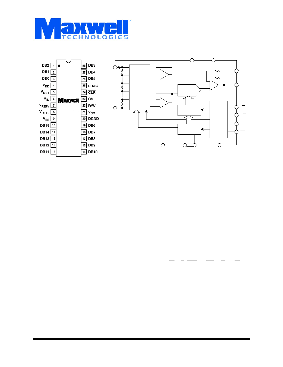
Maxwell Technologies' 7846A 16-Bit DAC converter microcir-
cuit features a greater than 100 krad (Si) total dose tolerance,
depending upon space mission. The 7846A has V
REF+
and
V
REF-
reference inputs and an on-chip output amplifier which
gives the option of unipolar or bipolar output. The 7846A uses
a segmented architecture. The 4 MSBs in the DAC latch
select one of the segments in a 16-resistor string. Both taps of
the segment are buffered by amplifiers and fed to a 12-bit
DAC, which provides a further 12 bits of resolution. This archi-
tecture ensures 16-bit monotonicity. Excellent integral linearity
results from tight matching between the input offset voltages
of the two buffer amplifiers. In addition to the excellent accu-
racy specifications, the 7846A also offers a comprehensive
microprocessor interface. There are 16 data I/O pins, plus
control lines (CS, R/W, LDAC and CLR). R/W and CS have
readback function which allows writing to and reading from the
I/O latch.
Maxwell Technologies' patented R
AD
-P
AK
® packaging technol-
ogy incorporates radiation shielding in the microcircuit pack-
age. It eliminates the need for box shielding while providing
the required radiation shielding for a lifetime in orbit or space
mission. In a GEO orbit, R
AD
-P
AK
provides greater than 100
krad (Si) radiation dose tolerance. This product is available
with screening up to Class S.
16
Segment
Switch
Matrix
Control
Logic
A2
A1
A3
I/O Latch
DAC Latch
12-bit DAC
-
+
-
+
-
+
R
R
6
5
23
22
25
24
20
3
10
9
8
7
21
4
V
DD
V
CC
V
REF+
V
REF-
V
SS
DB15
DB0
DGND
CLR
LDAC
R/W
CS
V
OUT
R
IN
12
12
4
R
R
R
Logic Diagram
7846A
M
e
m
o
r
y
2
All data sheets are subject to change without notice
©2003 Maxwell Technologies
All rights reserved.
16-Bit Digital to Analog Converter
7846A
05.29.03 REV 5
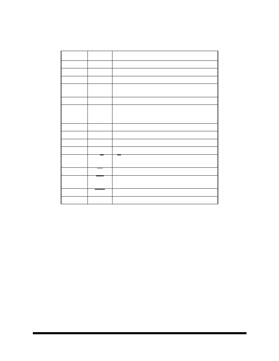
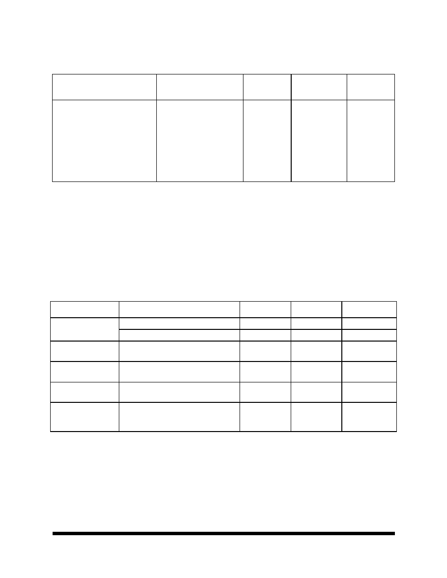
T
ABLE
1. 7846A P
INOUT
D
ESCRIPTION
P
IN
S
YMBOL
D
ESCRIPTION
1-3
DB2-DB0
Data I/O pins. DB0 is LSB.
4
V
DD
Positive supply for analog circuitry. This is +15V nominal.
5
V
OUT
DAC output voltage pin.
6
R
IN
Input to summing resistor of DAC output amplifier. This is used
to select output voltage ranges.
7
V
REF+
V
REF+
Input. The DAC is specified for V
REF+
= +5V.
8
V
REF-
V
REF-
Input. For unipolar operation connect V
REF-
to 0V and for
bipolar operation connect it to -5V. The device is specified for
both conditions.
9
V
SS
Negative supply for the analog circuitry. This is -15V nominal.
10-19
DB15-DB6
Data I/O pins. DB15 is MSB.
20
DGND
Ground pin for digital circuitry.
21
V
CC
Positive supply for digital circuitry. This is +5V nominal.
22
R/W
R/W Input. This can be used to load data to the DAC or to read
back the DAC latch contents.
23
CS
Chip select input. This selects the device.
24
CLR
Clear Input. The DAC can be cleared to 000...000 or
100...000.
25
LDAC
Asynchronous load input to DAC.
26-28
DB5-DB3
Data I/O pins.
M
e
m
o
r
y
3
All data sheets are subject to change without notice
©2003 Maxwell Technologies
All rights reserved.
16-Bit Digital to Analog Converter
7846A
05.29.03 REV 5
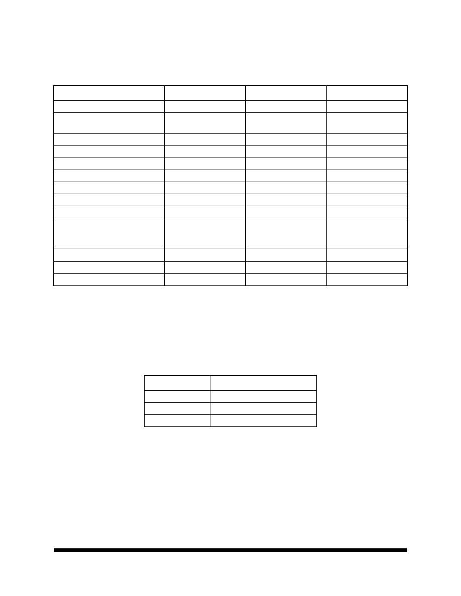
T
ABLE
2. 7846A A
BSOLUTE
M
AXIMUM
R
ATINGS
1
1. Stresses above those listed under "Absolute Maximum Ratings" may cause permanent damage to the device. This is a stress
rating only and functional operation of the device at these or any other conditions above those indicated in the operational sec-
tions of this specification is not implied. Exposure to absolute maximum rating conditions for extended periods of time may
affect device reliability. Only one absolute maximum rating may be applied at any one time.
P
ARAMETER
M
IN
M
AX
U
NIT
V
DD
to DGND
-0.3
+17
V
V
CC
to DGND
-0.3
V
DD
+0.3 or 7
(Whichever Is Lower)
V
V
SS
to DGND
-17
+0.3
V
V
REF+
to DGND
-25
+25
V
V
REF-
to DGND
-25
+25
V
V
OUT
to DGND
2
2. V
OUT
may be shorted to DGND, V
DD
, V
SS
and V
CC
provided that the power dissipation of the package is not exceeded.
-25
+25
V
R
IN
to DGND
-25
+25
V
Digital Input Voltage to DGND
-0.3
V
CC
+0.3
V
Digital Output Voltage to DGND
-0.3
V
CC
+0.3
V
Power Dissipation
To +75
°
C
Derates above +75
°
C
1000
10
mW
mW/
°
C
Thermal Inpedance
JC
2.78
°C
Operating Temperature Range
-55
+125
°
C
Storage Temperature Range
-65
+150
°
C
T
ABLE
3. D
ELTA
L
IMITS
P
ARAMETER
V
ARIATION
I
DD
±10% of value specified in Table 4.
I
EE
±10% of value specified in Table 4.
I
CC
±10% of value specified in Table 4.
M
e
m
o
r
y
4
All data sheets are subject to change without notice
©2003 Maxwell Technologies
All rights reserved.
16-Bit Digital to Analog Converter
7846A
05.29.03 REV 5
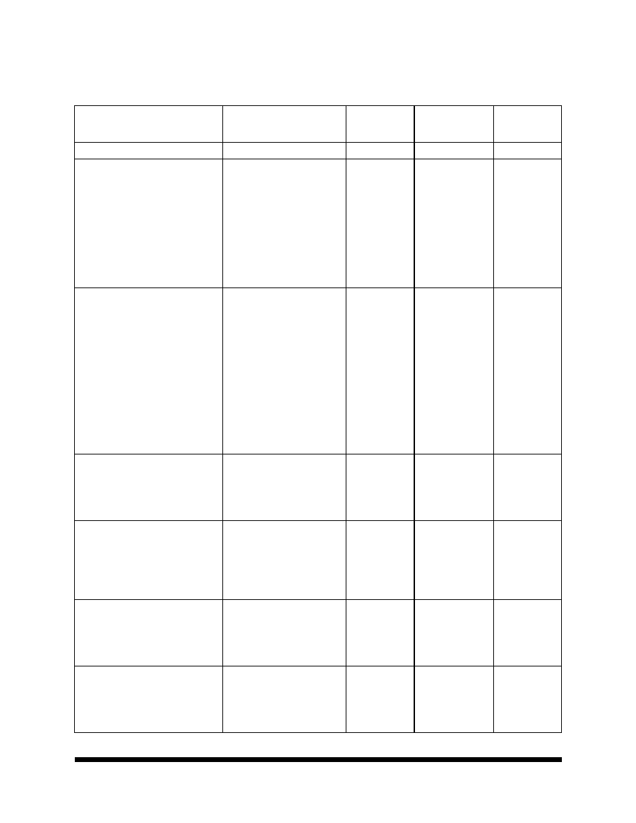
T
ABLE
4. 7846A E
LECTRICAL
S
PECIFICATIONS
1
(VDD=+15V ±5%; VSS=-15V ±5%; V
CC
= +5 V ±5%, T
A
= -55
TO
+125°C)
P
ARAMETER
T
EST
C
ONDITIONS
/C
OMMENTS
S
UBGROUPS
T
A
=-55
°
C
TO
+125
°
C
U
NIT
Resolution
16
Bits
UNIPOLAR OUTPUT
Relative Accuracy @ 25
°
C
- T
MIN
to T
MAX
Differential Nonlinearity Error
Gain Error @ 25
°
C
- T
MIN
to T
MAX
Offset Error @ 25
°
C
- T
MIN
to T
MAX
Gain TC
2
Offset TC
2
V
REF-
=0V, V
OUT
=0V to +10V
1LSB=153µ V
Guaranteed Monotonic
V
OUT
Load= 10M
1
2, 3
1
1
2,3
1
2,3
1
1
±16
±16
±1
±12
±24
±12
±24
±2
±2
LSB typ
LSB max
LSB max
LSB typ
LSB max
LSB typ
LSB max
ppm FSR/°C typ
ppm FSR/°C typ
BIPOLAR OUTPUT
Relative Accuracy @ 25
°
C
- T
MIN
to T
MAX
Differential Nonlinearity Error
Gain Error @ 25
°
C
- T
MIN
to T
MAX
Offset Error @ 25
°
C
- T
MIN
to T
MAX
Bipolar Zero Error @ 25
°
C
- T
MIN
to T
MAX
Gain TC
2
Offset TC
2
Bipolar Zero TC
2
V
REF-
=-5V, V
OUT
=-10V to +10V
1LSB=305µ V
Guaranteed Monotonic
V
OUT
Load=10M
V
OUT
Load=10M
1
2, 3
1
1
2, 3
1
2, 3
1
2, 3
1
1
1
±6
±8
±1
±6
±16
±6
±16
±6
±16
±2
±2
±2
LSB typ
LSB max
LSB max
LSB typ
LSB max
LSB typ
LSB max
LSB typ
LSB max
ppm FSR/
°
C typ
ppm FSR/
°
C typ
ppm FSR/
°
C typ
REFERENCE INPUT
Input Resistance
V
REF+
Range
V
REF-
Range
Resistance from V
REF-
to V
REF+
Typically 30k
1, 2, 3
20
40
V
SS
+ 6 to V
DD
- 6
V
SS
+ 6 to V
DD
- 6
K
min
K
max
V
V
OUTPUT CHARACTERISTICS
Output Voltage Swing
Resistive Load
1
Capacitive Load
3
Output Resistance
Short Circuit Current
To 0V
To 0V
To 0V or Any Power Supply
1, 2, 3
V
SS
+ 4 to V
DD
- 3
3
1000
0.3
±25
V max
k
min
pF max
typ
mA typ
DIGITAL INPUTS
V
IH
(Input High Voltage)
V
IL
(Input Low Voltage)
I
IN
(Input Current)
C
IN
(Input Capacitance)
2
1, 2, 3
2.4
0.8
±10
10
V min
V max
µ A max
pF max
DIGITAL OUTPUTS
V
OL
(Output Low Voltage)
V
OH
(Output High Voltage)
Floating State Leakage Current
Floating State Output Capacitance
2
I
SINK
= 1.6mA
I
SOURCE
= 400µ A
DB0-DB15 = 0 to V
CC
1, 2, 3
0.4
4.0
±10
10
V max
V min
µ A max
pF max
M
e
m
o
r
y
5
All data sheets are subject to change without notice
©2003 Maxwell Technologies
All rights reserved.
16-Bit Digital to Analog Converter
7846A
05.29.03 REV 5
POWER REQUIREMENTS
4
V
DD
V
SS
V
CC
I
DD
I
SS
I
CC
Power Supply Sensitivity
5
Power Dissipation
V
OUT
Unloaded
V
OUT
Unloaded
V
OUT
Unloaded
1, 2, 3
+11.4/+15.75
-11.4/-15.75
+4.75/+5.25
5
5
1
2
100
V min/V max
V min/V max
V min/V max
mA max
mA max
mA max
LSB/V max
mW typ
1. Minimum load is 3k
.
2. Sample tested to ensure compliance.
3. Maximum load is 1000pF.
4. 7846ARP is functional with power supplies of ±12V. See typical performance curves.
5. Sensitivity to Gain Error, Offset Error and Bipolar Zero Error to V
DD
, V
SS
variations.
6. Guaranteed by design
T
ABLE
5. 7846A AC P
ERFORMANCE
C
HARACTERISTICS1
(VDD=+15V ±5%; VSS=-15V ±5%; V
CC
= +5 V ±5%, T
A
= -55
TO
+125°C)
1. Guaranteed by design.
P
ARAMETER
T
EST
C
ONDITIONS
T
A
=25
°
C
T
A
=T
MIN
TO
T
MAX
U
NIT
Output Settling Time
To 0.006% FSR. V
OUT
loaded. V
REF-
=0V.
7
7
µ s max
To 0.003% FSR. V
OUT
loaded. V
REF-
=-5V.
9
9
µ s max
Digital-to-Analog Glitch
Impulse
DAC alternately loaded with 10...0000 and
01...1111. V
OUT
unloaded.
400
400
nV-secs typ
AC Feed through
V
REF-
=0V, V
REF+
=1V rms, 10kHz sine wave.
DAC loaded with all 0s.
0.5
0.5
mV pk-pk typ
Digital Feed through
DAC alternately loaded with all 1s and all
0s. CS High.
10
10
nV-secs typ
Output Noise Voltage
Density
(1kHz-100kHz)
Measured at V
OUT
. DAC loaded with
0111011...11.
V
REF+
=V
REF-
=0V.
50
50
nV/(Hz)
½
typ
T
ABLE
4. 7846A E
LECTRICAL
S
PECIFICATIONS
1
(VDD=+15V ±5%; VSS=-15V ±5%; V
CC
= +5 V ±5%, T
A
= -55
TO
+125°C)
P
ARAMETER
T
EST
C
ONDITIONS
/C
OMMENTS
S
UBGROUPS
T
A
=-55
°
C
TO
+125
°
C
U
NIT