 | ÐлекÑÑоннÑй компоненÑ: 7872RPFE | СкаÑаÑÑ:  PDF PDF  ZIP ZIP |
Äîêóìåíòàöèÿ è îïèñàíèÿ www.docs.chipfind.ru
1
M
e
m
o
r
y
All data sheets are subject to change without notice
(858) 503-3300 - Fax: (858) 503-3301 - www.maxwell.com
14-Bit A/D Converter
7872
©2001 Maxwell Technologies
All rights reserved.
5.21.02 Rev 4
F
EATURES
:
· 14-bit resolution and accuracy
· Total dose hardness:
- > 100 krad (Si), depending upon space mission
· Single event effects:
- SEL > 104 MeV/mg/cm
2
- SEU
TH
= 1.4 MeV/mg/cm
2
- SEU
Sat
= 1E-3 cm
2
/Device
· Package:
- 16 pin R
AD
-P
AK
® flat package
- 16 pin R
AD
-P
AK
® dual-in-line package
· Fast Conversion Times: 10 µ s
· Low 50 mW typical power consumption
· High speed LC
2
MOS technology
- Analog input range of ±3V
- 83 KSPS throughput rate
- Operates with +5V/-5V power supplies
- 80 dB SNR at 10 kHz input frequency
- 2 s complement coding
- Serial output
D
ESCRIPTION
:
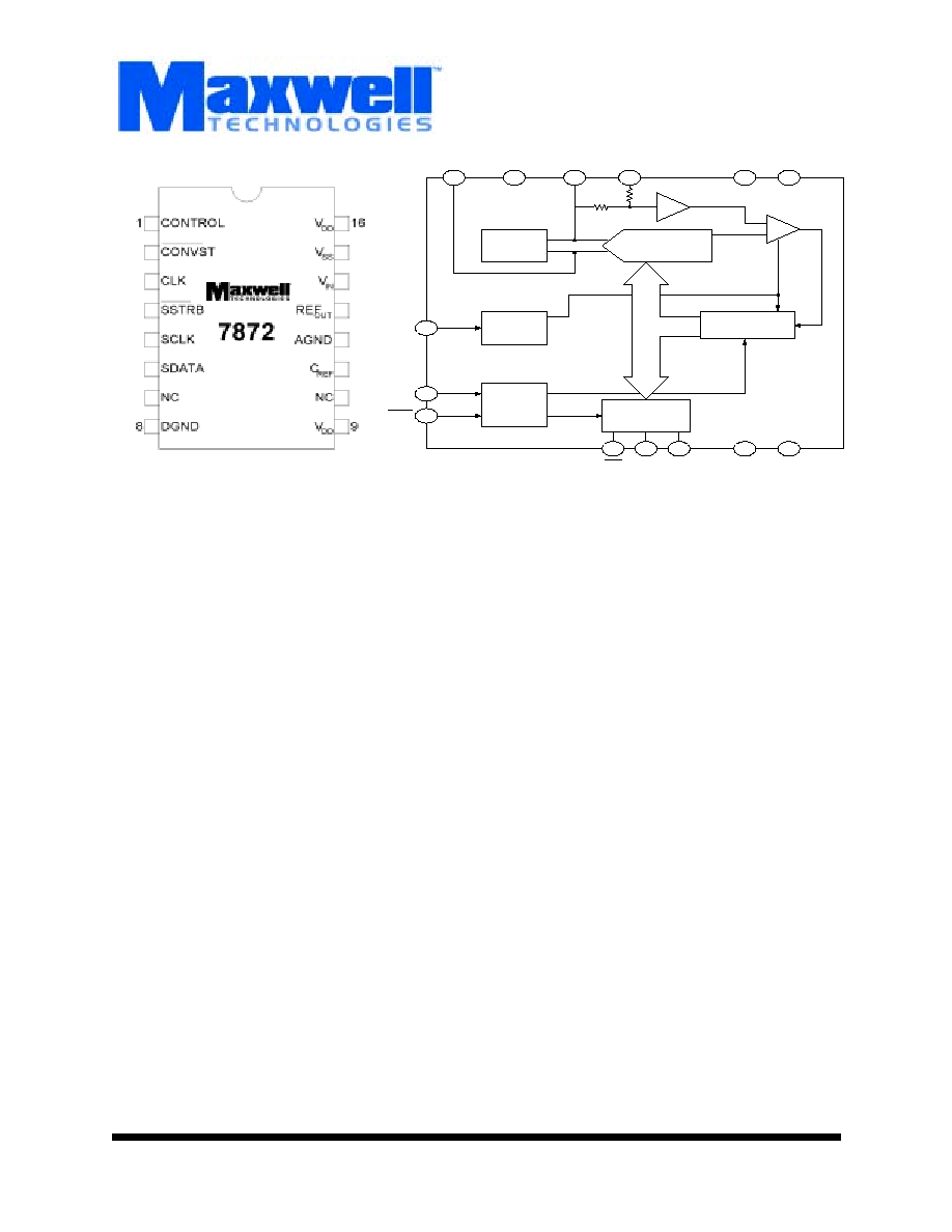
Maxwell Technologies' 7872 high-speed 14-bit ADC microcir-
cuit features a greater than 100 krad (Si) total dose tolerance;
depending upon orbit. The 7872 consists of a track/hold ampli-
fier, successive-approximation ADC, 3V buried Zener refer-
ence and versatile interface logic. It features a self-contained,
laser- trimmed internal clock, so no external clock timing com-
ponents are required. For minimum noise possible, the on-
chip clock may be overridden to synchronize the device oper-
ation to the digital system. The 7872 is a serial output device.
It is capable of interfacing to all modern microprocessors and
digital signal processors. The 7872 operates from ±5V power
supplies, accepts bipolar input signals of ±3V and is able to
convert full power signals up to 41.5 kHz. It is also fully speci-
fied for dynamic performance parameters including distortion
and signal-to-noise ratio.
Maxwell Technologies' patented R
AD
-P
AK
® packaging technol-
ogy incorporates radiation shielding in the microcircuit pack-
age. It eliminates the need for box shielding while providing
the required radiation shielding for a lifetime in orbit or space
mission. In a GEO orbit, R
AD
-P
AK
provides greater than 100
krad (Si) radiation dose tolerance. This product is available
with screening up to Class S.
3V
REFERENCE
CLOCK
CONTROL
LOGIC
14-BIT DAC
SERIAL
INTERFACE
12
11
13
14
9
16
3
1
2
4
5
6
SAR + COUNTER
8
15
R
R
TRACK/HOLD
COMP
AGND
C
REF
REF OUT
V
IN
V
DD
V
DD
CLK
CONTROL
CONVST
SSTRB
SCLK
SDATA
DGND
V
SS
Logic Diagram
M
e
m
o
r
y
2
All data sheets are subject to change without notice
©2001 Maxwell Technologies
All rights reserved.
14-Bit A/D Converter
7872
5.21.02 Rev 4
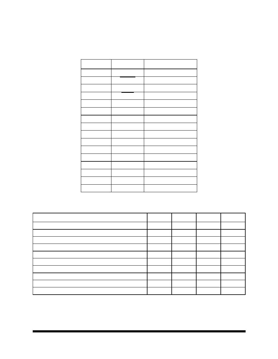
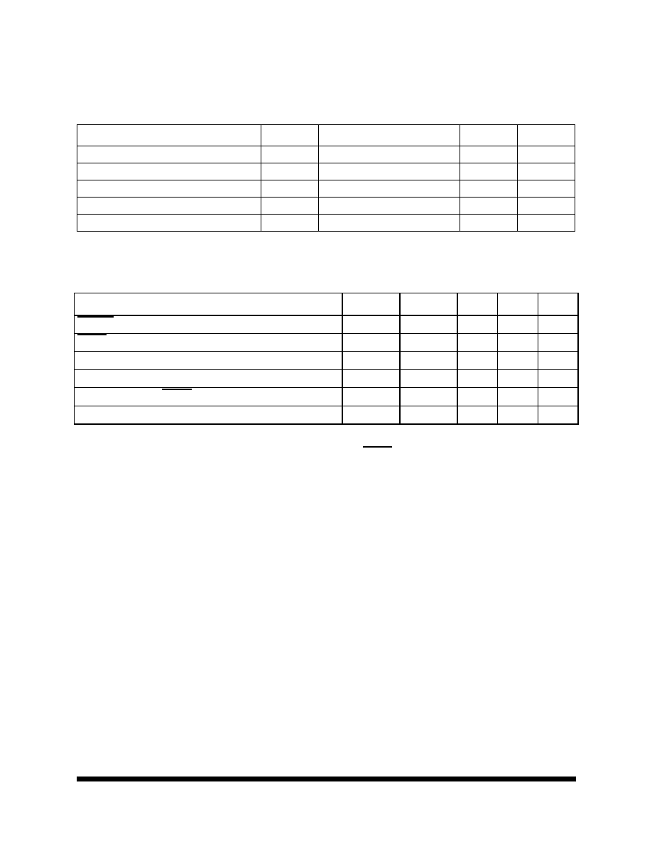
T
ABLE
1. 7872 P
IN
D
ESCRIPTION
P
IN
S
IGNAL
D
ESCRIPTION
1
CONTROL
Control Function
2
CONVST
Convert Start
3
CLK
Clock Input
4
SSTRB
Serial Strobe
5
SCLK
Serial Clock
6
SDATA
Serial Data
7
NC
Non Connect
8
DGND
Digital Ground
9
V
DD
Positive Supply
10
NC
No Connect
11
C
REF
Reference Capacitor
12
AGND
Analog Ground
13
REF
OUT
Voltage Reference Output
14
V
IN
Analog Input
15
V
SS
Negative Supply
16
V
DD
Positive Supply
T
ABLE
2. 7872 A
BSOLUTE
M
AXIMUM
R
ATINGS
P
ARAMETER
S
YMBOL
M
IN
M
AX
U
NIT
Positive Supply Voltage; Relative to GND
V
DD
-0.3
7.0
V
Negative Supply Voltage; Relative to GND
V
SS
0.3
7.0
V
AGND to DGND; Relative to GND
--
-0.3
V
DD
+0.3
V
REF
OUT
, C
REF
to AGND
--
0
V
DD
V
V
IN
to AGND
--
V
SS
-0.3
V
DD
+0.3
V
Digital Input Voltage
V
IN
-0.3
V
DD
+0.3
V
Digital Output Voltage
V
OUT
-0.3
V
DD
+0.3
V
Thermal Impedance
JC
--
2.44
°C/W
Storage Temperature Range
T
S
-65
150
°C
Operating Temperature Range
T
A
-55
125
°C
M
e
m
o
r
y
3
All data sheets are subject to change without notice
©2001 Maxwell Technologies
All rights reserved.
14-Bit A/D Converter
7872
5.21.02 Rev 4
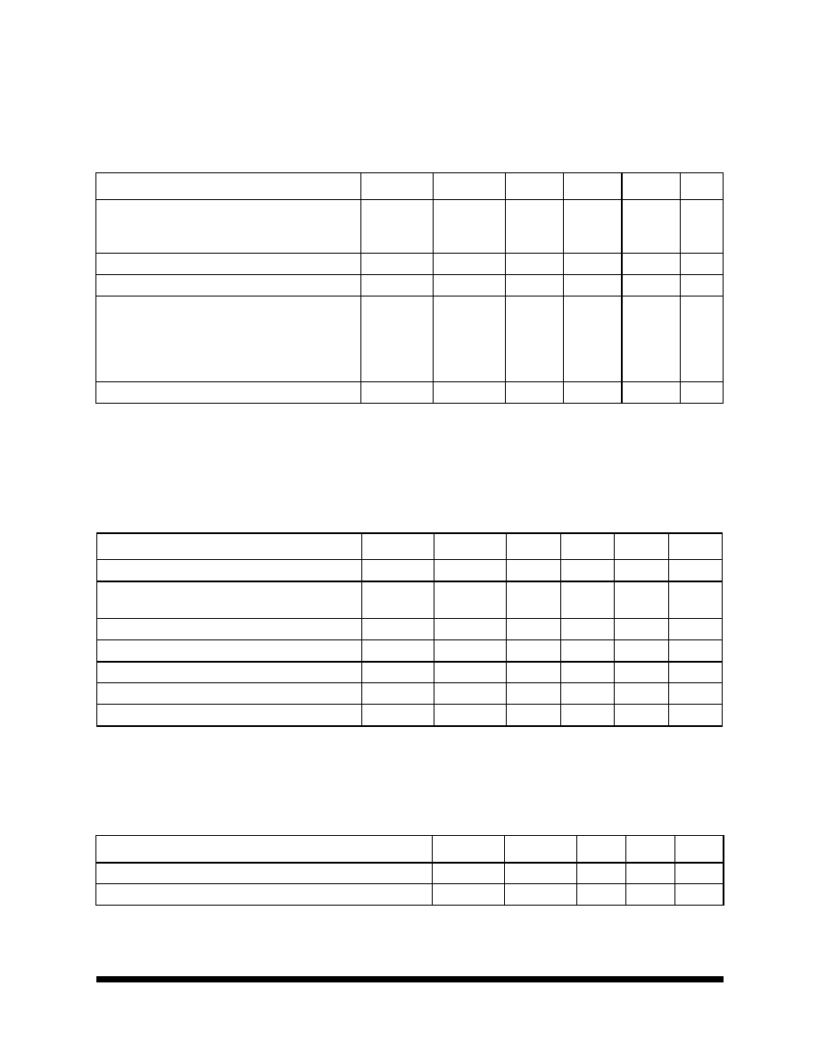
T
ABLE
3. 7872 DC E
LECTRICAL
C
HARACTERISTICS
FOR
D
YNAMIC
P
ERFORMANCE
1
(V
DD
= 5 V ± 5%, V
SS
= -5 V ± 5%, AGND = DGND = 0 V,
f
CLK
= 2 MH
Z
EXTERNAL
, f
SAMPLE
= 83
K
H
Z
, -55
TO
125
°
C
UNLESS
OTHERWISE
SPECIFIED
)
1. V
IN
= ± 3 V. Guaranteed by design.
P
ARAMETER
S
YMBOL
S
UBGROUPS
M
IN
T
YP
M
AX
U
NIT
Signal to Noise Ratio V
IN
= 10kHz Sine Wave, T
MIN
to
T
MAX
;
SNR is typically 82dB for V
IN
< 41.5kHz
2
2. SNR calculation includes distortion and noise components.
SNR
4, 5, 6
79
--
--
dB
Total Harmonic Distortion V
IN
= 10kHz Sine Wave
THD
4, 5, 6
--
-86
--
dB
Peak Harmonic or Spurious Noise
--
4, 5, 6
--
-86
--
dB
Intermodulation Distortion
Second Order Terms: f
a
= 9 kHz, f
b
= 9.5 kHz, f
SAMPLE
= 50 kHz
Third Order Terms: f
a
= 9 kHz, f
b
= 9.5 kHz, f
SAMPLE
=
50 kHz
IMD
4, 5, 6
--
--
-86
-86
--
--
dB
Track/Hold Acquisition Time
--
4, 5, 6
--
--
2
µ s
T
ABLE
4. 7872 DC E
LECTRICAL
C
HARACTERISTICS
FOR
A
CCURACY
(V
DD
= 5V ±5%, V
SS
= -5 V ± 5%, T
A
= -55
TO
125 °C
UNLESS
OTHERWISE
SPECIFIED
)
P
ARAMETER
S
YMBOL
S
UGROUPS
M
IN
T
YP
M
AX
U
NIT
Resolution
--
1, 2, 3
14
--
--
Bits
Resolution for Which No Missing Codes are Guaran-
teed
--
1, 2, 3
14
--
--
Bits
Integral Nonlinearity @ 25
°
C
--
1, 2, 3
--
±1
--
LSB
Integral Nonlinearity T
MIN
to T
MAX
--
1, 2, 3
--
--
±2
LSB
Bipolar Zero Error
--
1, 2, 3
--
--
±12
LSB
Positive Gain Error
1
1. Measured with respect to internal reference.
--
1, 2, 3
--
--
±12
LSB
Negative Gain Error
1
--
1, 2, 3
--
--
±12
LSB
T
ABLE
5. 7872 DC E
LECTRICAL
C
HARACTERISTICS
FOR
A
NALOG
I
NPUT
(V
DD
= 5V ±5%, V
SS
= -5 V ± 5%, T
A
= -55
TO
125 °C
UNLESS
OTHERWISE
SPECIFIED
)
P
ARAMETER
S
YMBOL
S
UBGROUPS
M
IN
M
AX
U
NITS
Input Voltage Range
--
1, 2, 3
-3
3
V
Input Current
--
1, 2, 3
-500
500
µ A
M
e
m
o
r
y
4
All data sheets are subject to change without notice
©2001 Maxwell Technologies
All rights reserved.
14-Bit A/D Converter
7872
5.21.02 Rev 4
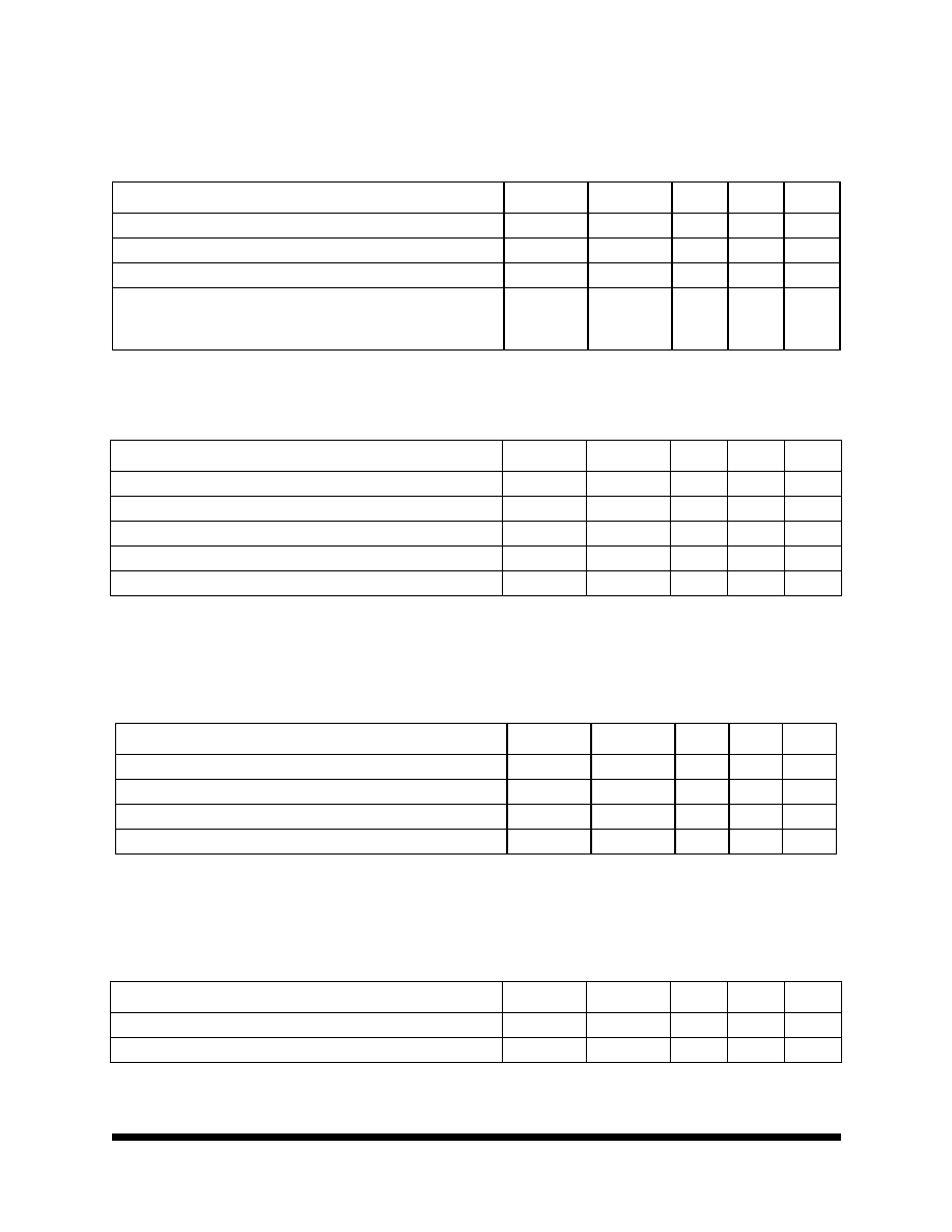
T
ABLE
6. 7872 DC E
LECTRICAL
C
HARACTERISTICS
FOR
R
EFERENCE
O
UTPUT
(V
DD
= 5V ±5%, V
SS
= -5 V ± 5%, T
A
= -55
TO
125 °C
UNLESS
OTHERWISE
SPECIFIED
)
P
ARAMETER
S
YMBOL
S
UGGROUPS
M
IN
M
AX
U
NIT
REF
OUT
@ +25
°
C
--
1, 2, 3
2.99
3.01
V
REF
OUT
T
MIN
to T
MAX
--
1, 2, 3
2.98
3.02
V
REF
OUT
Tempco: Typically 35ppm
--
1, 2, 3
--
±40
ppm/
o
C
Reference Load Sensitivity (DREF
OUT
/DI) Reference Load Current
Change (0-300 µ A); Reference Load Should Not Be Changed Dur-
ing Conversion
--
1, 2, 3
--
1.2
mV
T
ABLE
7. 7872 DC E
LECTRICAL
C
HARACTERISTICS
FOR
L
OGIC
I
NPUTS
(V
DD
= 5V ±5%, V
SS
= -5 V ± 5%, T
A
= -55
TO
125 °C
UNLESS
OTHERWISE
SPECIFIED
)
P
ARAMETER
S
YMBOL
S
UGGROUPS
M
IN
M
AX
U
NIT
Input High Voltage: V
DD
5 V ± 5%
V
INH
1, 2, 3
2.4
--
V
Input Low Voltage: V
DD
5 V ± 5%
V
INL
1, 2, 3
--
0.8
V
Input Current: V
IN
= 0 V to V
DD
I
IN
1, 2, 3
-10
10
µ A
Input Current: (14/8/CLK input only) VIN = VSS to VDD
--
1, 2, 3
-10
10
µ A
Input Capacitance
1
1. Not tested.
C
IN
1, 2, 3
--
10
pF
T
ABLE
8. 7872 DC E
LECTRICAL
C
HARACTERISTICS
FOR
L
OGIC
O
UTPUTS
(V
DD
= 5V ±5%, V
SS
= -5 V ± 5%, T
A
= -55
TO
125 °C
UNLESS
OTHERWISE
SPECIFIED
)
P
ARAMETER
S
YMBOL
S
UBGROUPS
M
IN
M
AX
U
NIT
Output High Voltage I
SOURCE
= 40 µ A
V
OH
1, 2, 3
4.0
--
V
Output Low Voltage I
SINK
= 1.6 mA
V
OL
1, 2, 3
--
0.4
V
Floating-State Leakage Current
--
1, 2, 3
--
10
µ A
Floating-State Output Capacitance
1
1. Not tested.
--
1, 2, 3
--
15
pF
T
ABLE
9. 7872 DC E
LECTRICAL
C
HARACTERISTICS
FOR
C
ONVERSION
T
IME
(V
DD
= 5V ±5%, V
SS
= -5 V ± 5%, T
A
= -55
TO
125 °C
UNLESS
OTHERWISE
SPECIFIED
)
P
ARAMETER
S
YMBOL
S
UBGROUPS
M
IN
M
AX
U
NIT
External Clock
--
1, 2, 3
--
10
µ s
Internal Clock: Nominal Value = 2 MHz
--
1, 2, 3
--
11
µ s
M
e
m
o
r
y
5
All data sheets are subject to change without notice
©2001 Maxwell Technologies
All rights reserved.
14-Bit A/D Converter
7872
5.21.02 Rev 4
T
ABLE
10. 7872 DC E
LECTRICAL
C
HARACTERISTICS
FOR
P
OWER
R
EQUIREMENTS
(V
DD
= 5V ±5%, V
SS
= -5 V ± 5%, T
A
= -55
TO
125 °C
UNLESS
OTHERWISE
SPECIFIED
)
P
ARAMETER
S
YMBOL
C
ONDITIONS
R
EQUIREMENTS
U
NITS
Positive Supply Voltage
V
DD
5% for Specified Performance
5
V
Negative Supply Voltage
V
SS
5% for Specified Performance
-5
V
Positive Supply Current
I
DD
Typically 6mA
13
mA max
Negative Supply Current
I
SS
Typically 4mA
6
mA max
Power Dissipation
P
D
Typically 50mW
95
mW max
T
ABLE
11. 7872 T
IMING
C
HARACTERISTICS
1,2
(V
DD
= 5V ±5%, V
SS
= -5 V ± 5%, T
A
= -55
TO
125 °C
UNLESS
OTHERWISE
SPECIFIED
)
1. All input signals are specified with tr = tr = 5 ns (10% to 90% of 5 V) and timed from a voltage level of 1.6 V.
2. Serial timing is measured with a 4.7 k
pull-up resistor on SDATA and SSTRB and a 2 k
pull-up resistor on SCLK. The
capacitance on all three outputs is 35 pF.
P
ARAMETER
/C
ONDITION
S
YMBOL
S
UBGROUPS
M
IN
M
AX
U
NITS
CONVST Pulse Width
t
1
9, 10, 11
50
--
ns
SSTRB to SCLK Falling Edge Setup Time
t
10
9, 10, 11
100
--
ns
SCLK Cycle Time
3
3. SCLK mark/space ration (measured from a voltage level of 1.6 V) is 40/60 to 60/40.
t
11
9, 10, 11
440
--
ns
SCLK to Valid Data Delay: C
L
= 35 pF
4
4. SDATA will drive higher capacitive loads, but this will add to t
12
since it increases the external RC time constant (4.7k
/C
L
) and
hence, the time to reach 2.4 V.
t
12
9, 10, 11
--
155
ns
SCLD Rising Edge to SSTRB
t
13
9, 10, 11
20
150
ns
Bus Relinquish Time After SCLK
t
14
9, 10, 11
4
100
ns
Document Outline