 | –≠–ª–µ–∫—Ç—Ä–æ–Ω–Ω—ã–π –∫–æ–º–ø–æ–Ω–µ–Ω—Ç: 903RPFI | –°–∫–∞—á–∞—Ç—å:  PDF PDF  ZIP ZIP |
1
Memory
All data sheets are subject to change without notice
(858)503-3000 Fax:(858)503-3301 www.maxwell.com
©2002 Maxwell Technologies
All rights reserved.
09.12.02 REV 1
903
High Speed Comparator
F
EATURES
:
∑ High-speed, low-power voltage comparator
∑
R
AD
-P
AK
Æ radiation-hardened against
natural space radiation
∑ Total dose hardness: 100 krad (Si) typical;
dependent upon orbit
∑ 8ns typ propagation delay
∑ 18mW power consumption (typ at +5V)
∑ Separate analog and digital supplies
∑ Flexible analog supply: +5V to +10V or ±5V
∑ Input range includes negative supply rail
∑ TTL compatible outputs
∑ TTL compatible latch inputs
D
ESCRIPTION
:
Maxwell Technologies' 903
high-speed, low-
power voltage comparator features differential
analog inputs and TTL logic outputs with
active internal pull-ups. The 903 can be pow-
ered from separate analog and digital power
supplies or from a single combined supple
voltage. The analog input common-mode
range includes the negative rail, allowing
ground sensing when powered from a single
supply. When powered from +5V, the 903 con-
sumes 18mW. The 903 is equipped with a TTL
compatible latch input. The comparator output
is latched when the latch input is driven low.
Capable of surviving space environments, the
903 is ideal for satellite, spacecraft, and space
probe missions. Maxwell Technologies' pat-
ented
R
AD
-P
AK
Æ packaging technology incor-
porates radiation shielding in the microcircuit
package. It eliminates box shielding while pro-
viding lifetime in orbit or space mission. In
GEO orbit, RAD-PAKÆ provides greater than
100 krad(Si) radiation dose rate. This product
is available with screening up to Class S.
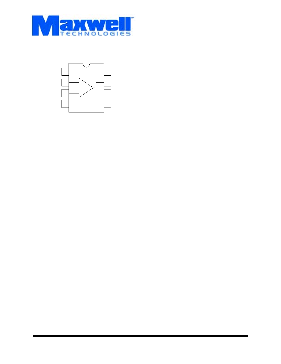
8
7
6
5
+
-
1
4
2
3
V
CC
V
EE
IN+
IN-
V
DD
LATCH
OUT
GND

Memory
2
09.12.02 REV 1
All data sheets are subject to change without notice
©2002 Maxwell TechnologiesAll
rights reserved.
High-Speed Comparator
903
T
ABLE
1. P
INOUT
D
ESCRIPTION
P
IN
N
AME
F
UNCTION
1
V
CC
Positive Analog Supply
2
IN+
Positive input
3
IN-
Negative input
4
V
EE
Negative analog supply and substrate
5
LATCH
Latch input
6
GND
Ground terminal
7
OUT
Output
8
V
DD
Positive digital supply
T
ABLE
2. A
BSOLUTE
M
AXIMUM
R
ATINGS
P
ARAMETER
M
IN
M
AX
U
NITS
Analog Supply Voltage (V
CC
to V
EE
)
--
+12
V
Digital Supply Voltage (V
DD
to GND)
--
+7
V
Differential Input Voltage
V
EE
- 0.2
V
CC
+ 0.2
V
Common-mode Input Voltage
V
EE
- 0.2
V
CC
+ 0.2
V
Latch Input Voltage
-0.2
V
DD
+ 0.2
V
Output Short-circuit Duration to GND
Output Short-circuit Duration to V
DD
Indefinite
--
1
min.
Operating Temperature Ranges
-55
+125
∞C
Junction Temperature (Tj)
-65
+160
∞C
Storage Temperature Range
-65
+150
∞C
T
ABLE
3. AC E
LECTRICAL
C
HARACTERISTICS
(V
CC
= +5V, V
EE
= -5V, L
ATCH
= L
OGIC
H
IGH
, T
A
= T
MIN
TO
T
MAX
,
UNLESS
OTHERWISE
SPECIFIED
)
P
ARAMETER
S
YMBOL
T
EST
C
ONDITIONS
S
UB
G
ROUPS
M
IN
T
YP
M
AX
U
NITS
Input-to-output High Response Time
tpd+
VOD = 5mV,
CL = 15pF,
IO = 2mA
1
9, 10, 11
--
10
15
ns
Input-to-output Low Response Time
tpd-
VOD = 5mV,
CL = 15pF,
IO = 2mA
1
9, 10, 11
--
10
15
ns
Memory
3
09.12.02 REV 1
All data sheets are subject to change without notice
©2002 Maxwell TechnologiesAll
rights reserved.
High-Speed Comparator
903
Latch Disable to
Output High Delay
tpd+
2
9, 10, 11
10
ns
Latch Disable to
Output Low Delay
tpd-
2
9, 10, 11
12
ns
Minimum Setup Time
ts
2
9, 10, 11
2
ns
Minimum Hold Time
th
2
9, 10, 11
1
ns
Minimum Latch
Disable Pulse Width
tpw
2
9, 10, 11
10
ns
1. Guaranteed by design.
2. Owing to the difficult and critical nature of switching measurements involving the latch, these parameters cannot
be tested in a production environment. Typical specifications listed are taken from measurements using a high-
speed test fixture.
T
ABLE
4. DC E
LECTRICAL
C
HARACTERISTICS
(V
CC
= +5V, V
EE
= -5V, L
ATCH
= L
OGIC
H
IGH
, T
A
= T
MIN
TO
T
MAX
U
NLESS
O
THERWISE
S
PECIFIED
)
P
ARAMETER
S
YMBO
L
T
EST
C
ONDITIONS
S
UBGROUP
S
M
IN
T
YP
M
AX
U
NITS
Input Offset Voltage
V
OS
V
CM
= 0V,
V
O
= 1.4V
1, 2, 3
--
2
6
mV
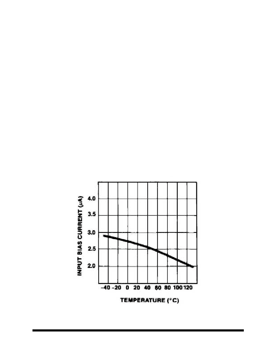
Input Bias Current
I
B
I
IN+
or I
IN-
1, 2, 3
--
6
15
µA
Input Offset Current
I
OS
V
CM
= 0V,
V
O
= 1.4V
1, 2, 3
--
200
800
nA
Input Voltage Range
V
CM
1
1, 2, 3
V
EE
-
0.1
--
V
CC
-
2.25
V
Common-mode Rejection Ratio
CMRR
-5V < V
CM
<
+2.75,
V
O
= 1.4V,
2
1, 2, 3
--
120
500
µV/V
Power-supply Rejection Ratio
PSRR
2
1, 2, 3
--
150
500
µV/V
Output High Voltage
V
OH
V
IN
> 250mV,
I
SRC
= 1mA
1, 2, 3
2.4
3.5
--
V
Output Low Voltage
V
OL
V
IN
> 250mV,
I
SINK
= 8mA
1, 2, 3
--
0.3
0.4
V
Latch Input Voltage High
V
LH
1, 2, 3
--
1.4
2.0
V
Latch Input Voltage Low
V
LL
1, 2, 3
0.8
1.4
--
V
Latch Input Current High
I
LH
V
LH
= 3.0V
1, 2, 3
--
1
20
µA
Latch Input Current Low
I
LL
V
LL
= 0.3V
1, 2, 3
--
1
20
µA
T
ABLE
3. AC E
LECTRICAL
C
HARACTERISTICS
(V
CC
= +5V, V
EE
= -5V, L
ATCH
= L
OGIC
H
IGH
, T
A
= T
MIN
TO
T
MAX
,
UNLESS
OTHERWISE
SPECIFIED
)
P
ARAMETER
S
YMBOL
T
EST
C
ONDITIONS
S
UB
G
ROUPS
M
IN
T
YP
M
AX
U
NITS
Memory
4
09.12.02 REV 1
All data sheets are subject to change without notice
©2002 Maxwell TechnologiesAll
rights reserved.
High-Speed Comparator
903
Positive Analog Supply Current
I
CC
1, 2, 3
--
2.5
6
mA
Negative Analog Supply Current
I
EE
1, 2, 3
--
2
5
mA
Digital Supply Current
I
DD
1, 2, 3
--
1
2.5
mA
Power Dissipation
P
D
V
CC
= V
DD
= +5V,
V
EE
= 0V
1, 2, 3
--
18
28
mW
1. The input common-mode voltage or either input signal voltage should not be allowed to go negative by
more than 0.2V below V
EE
. The upper end of the common-mode voltage range is typically V
CC
-0.2V, but
either or both inputs can go to a maximum of V
CC
+0.2V without damage.
2. Tested for +4.75V<V
CC
<+5.25V, and -5.25V<V
EE
<-4.75V with V
DD
= +5V, although permissible analog
power-supply range is +4.75V<V
CC
<+10.5V for single-supply operation with V
EE
grounded.
T
ABLE
4. DC E
LECTRICAL
C
HARACTERISTICS
(V
CC
= +5V, V
EE
= -5V, L
ATCH
= L
OGIC
H
IGH
, T
A
= T
MIN
TO
T
MAX
U
NLESS
O
THERWISE
S
PECIFIED
)
P
ARAMETER
S
YMBO
L
T
EST
C
ONDITIONS
S
UBGROUP
S
M
IN
T
YP
M
AX
U
NITS
Memory
5
09.12.02 REV 1
All data sheets are subject to change without notice
©2002 Maxwell TechnologiesAll
rights reserved.
High-Speed Comparator
903
F
IGURE
1. I
NPUT
O
FFSET
V
OLTAGE
VS
. T
EMPERATURE
F
IGURE
2. I
NPUT
B
IAS
C
URRENT
VS
. T
EMPERATURE