 | –≠–ª–µ–∫—Ç—Ä–æ–Ω–Ω—ã–π –∫–æ–º–ø–æ–Ω–µ–Ω—Ç: OP400RPFE | –°–∫–∞—á–∞—Ç—å:  PDF PDF  ZIP ZIP |
1
Memory
All data sheets are subject to change without notice
(858) 503-3300 - Fax: (858) 503-3301 - www.maxwell.com
Quad Low-Offset, Low-Power
Operational Amplifier
©2001 Maxwell Technologies
All rights reserved.
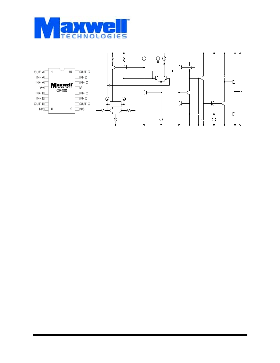
OP400
09.12.02 REV 5
VOL T AGE
LIMIT ING
NET WORK
+IN
-IN
BIAS
v+
v-
OUT
F
EATURES
:
∑ R
AD
-P
AK
Æ technology-hardened against natural space
∑ radiation
∑ Total dose hardness:
- > 100 krad (Si), depending upon space mission
∑ Package:
- 16 pin Rad-PakÆ flat package
∑ Low input offset voltage 150µ V max
∑ Low offset voltage drift
- +1.2µ V/∞C max (over -55 to +125∞C)
∑ Low supply current (per amplifier) 725 µ A max
∑ High open-loop gain 5000V/mV min
∑ Input bias current 3 nA Max
∑ Low noise voltage density 11 nV per (Hz)
Ω
at 1 kHz
∑ Stable with large capacitive loads 10 nF typ
D
ESCRIPTION
:
Maxwell Technologies' OP400 monolithic quad operational
amplifier microcircuit features a greater than 100 krad (Si) typ-
ical total dose tolerance, depending upon space mission.
Using Maxwell's radiation-hardened R
AD
-P
AK
Æ packaging
technology, the OP400 has an extremely low input offset volt-
age no less than 150 mV with a drift of under 1.2 mV/∞C, guar-
anteed over the full military temperature range. The OP400
features low power consumption, drawing less than 725 µ A
per amplifier.
Maxwell Technologies' patented R
AD
-P
AK
packaging technol-
ogy incorporates radiation shielding in the microcircuit pack-
age. It eliminates the need for box shielding while providing
the required radiation shielding for a lifetime in orbit or space
mission. In a GEO orbit, R
AD
-P
AK
provides greater than 100
krad (Si) radiation dose tolerance. This product is available
with screening up to Class S.
Logic Diagram
OP400
Memory
2
All data sheets are subject to change without notice
©2001 Maxwell Technologies
All rights reserved.
Quad Low-Offset, Low-Power Operational Amplifier
09.12.02 REV 5
T
ABLE
1. P
INOUT
D
ESCRIPTION
P
IN
S
YMBOL
D
ESCRIPTION
1, 7, 10, 16
OUT A - D
Output Signal
2, 6, 11, 15
-IN A - D
Negative Input Signal
3, 5, 12, 14
+IN A - D
Positive Input Signal
8, 9
NC
Not Connected
4
V+
Positive Voltage
13
V-
Negative Voltage
T
ABLE
2. OP400 A
BSOLUTE
M
AXIMUM
R
ATINGS
P
ARAMETER
S
YMBOL
M
IN
M
AX
U
NIT
Supply Voltage
V
CC
±20
V
Differential Input Voltage
±30
V
Input Voltage
Supply Voltage
Output Short-Circuit Duration
Continuous
Storage Temperature Range
T
S
-65
150
∞C
Operating Temperature Range
T
A
-55
125
∞C
T
ABLE
3. D
ELTA
L
IMITS
P
ARAMETER
V
ARIATION
ICC
±10% of specified value in Table 4
T
ABLE
4. OP400 DC E
LECTRICAL
C
HARACTERISTICS
(V
S
= ±15V, T
A
= -55
TO
125∞C,
UNLESS
OTHERWISE
SPECIFIED
)
P
ARAMETER
S
YMBOL
T
EST
C
ONDITIONS
S
UBGROUPS
M
IN
T
YP
M
AX
U
NITS
Input Offset Voltage
V
OS
+25∞C
1
---
40
150
µ V
-55 to 125∞C
2, 3
--
70
270
Long Term Input Voltage Stability
---
1, 2, 3
---
0.1
---
µ V/mo
Input Offset Current
I
OS
V
CM
= 0V
+25∞C
1
---
0.1
1.0
nA
-55 to 125∞C
2, 3
0.1
2.5
Input Bias Current
I
B
V
CM
= 0V
+25∞C
1
---
0.75
3.0
nA
-55 to 125∞C
2, 3
1.30
5.0
OP400
Memory
3
All data sheets are subject to change without notice
©2001 Maxwell Technologies
All rights reserved.
Quad Low-Offset, Low-Power Operational Amplifier
09.12.02 REV 5
Input Resistance Differential
Mode
R
IN
+25∞C
+25E = Engi-
neering (test-
ing @ +25∞C)
1
---
10
---
M
Input Resistance Common Mode
R
INCM
1, 2, 3
---
200
---
G
Large Signal Voltage Gain
A
VO
V
O
= ±10V
RL = 10
k
+25∞C
1
5000
12000
---
V/mV
-55 to 125∞C
2, 3
3000
9000
--
R
L
= 2 k
+25∞C
1
2000
3500
---
-55 to 125∞C
2, 3
1000
2300
--
Input Voltage Range
1
IVR
3/
+25∞C
1
±12
±13
---
V
-55 to 125∞C
2, 3
±12
±12.5
--
Common Mode Rejection
CMR
V
CM
=
±12V
+25∞C
4
120
140
---
dB
-55 to 125∞C
5, 6
115
130
--
Power Supply Rejection Ratio
PSRR
V
S
= ±3V
to ±18V
+25∞C
1
---
0.1
1.8
µ V/V
-55 to 125∞C
2, 31
--
0.2
3.2
Output Voltage Swing
V
O
R
L
= 10
k
1, 2, 3
±12
±12.6
---
V
R
L
= 2 k
1, 2, 3
±11
±12.4
---
Supply Current Per Amplifier
I
SV
No Load
+25∞C
1
---
600
725
µ A
-55 to 125∞C
2, 3
--
600
775
Input Capacitance
C
IN
+25∞C
1
---
3.2
---
pF
Capacitive Load Stability
AV = +1
No Oscilla-
tions
+25∞C
1
---
10
---
nF
1. Guaranteed by CMR test.
T
ABLE
5. OP400 AC Electrical Characteristics
(VS = ±15V, T
A
= -55
TO
125∞C,
UNLESS
OTHERWISE
SPECIFIED
.)
P
ARAMETER
S
YMBOL
Test Conditions
S
UBGROUP
M
IN
T
YP
M
AX
U
NIT
Input Noise Voltage
e
n p-p
0.1 Hz to 10 Hz
+25∞C
1
---
0.5
---
µ V
P-P
Input Noise Voltage
Density
e
n
f
O
= 10 Hz
+25∞C
1
---
22
--
nV
Hz
f
O
= 1 KHz
+25∞C
1
---
11
--
Input Noise Current
i
n p-p
0.1 Hz to 10 Hz
+25∞C
1
---
15
---
pA
P-P
Input Noise Current
Density
i
n
f
O
= 10 Hz
+25∞C
1
---
0.6
---
nV
Hz
Slew Rate
SR
-55 to 125∞C
1, 2, 3
0.1
0.15
---
V/µ s
Gain Bandwidth Product
GBWP A
V
= +1
-55 to 125∞C
1, 2, 3
---
500
---
kHz
T
ABLE
4. OP400 DC E
LECTRICAL
C
HARACTERISTICS
(V
S
= ±15V, T
A
= -55
TO
125∞C,
UNLESS
OTHERWISE
SPECIFIED
)
P
ARAMETER
S
YMBOL
T
EST
C
ONDITIONS
S
UBGROUPS
M
IN
T
YP
M
AX
U
NITS

OP400
Memory
4
All data sheets are subject to change without notice
©2001 Maxwell Technologies
All rights reserved.
Quad Low-Offset, Low-Power Operational Amplifier
09.12.02 REV 5
Channel Separation
CS
V
O
= 20 V
p-p
f
O
= 10 Hz
1
+25∞C
4
123
135
---
dB
1. Guaranteed by design.
T
ABLE
5. OP400 AC Electrical Characteristics
(VS = ±15V, T
A
= -55
TO
125∞C,
UNLESS
OTHERWISE
SPECIFIED
.)
P
ARAMETER
S
YMBOL
Test Conditions
S
UBGROUP
M
IN
T
YP
M
AX
U
NIT

OP400
Memory
5
All data sheets are subject to change without notice
©2001 Maxwell Technologies
All rights reserved.
Quad Low-Offset, Low-Power Operational Amplifier
09.12.02 REV 5
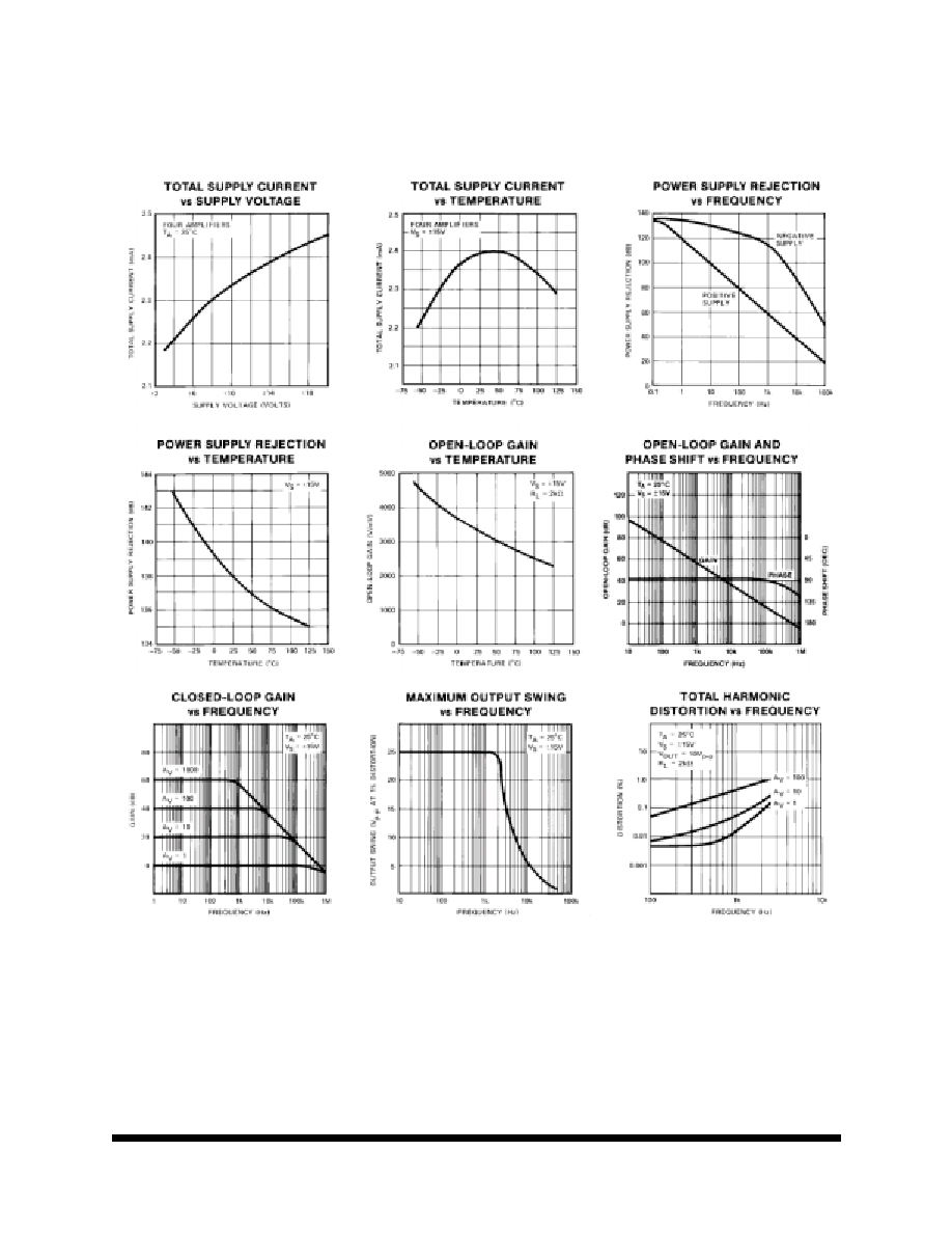
OP400 T
YPICAL
O
PERATING
C
HARACTERISTICS
OP400
Memory
6
All data sheets are subject to change without notice
©2001 Maxwell Technologies
All rights reserved.
Quad Low-Offset, Low-Power Operational Amplifier
09.12.02 REV 5
OP400 T
YPICAL
O
PERATING
C
HARACTERISTICS
(C
ONTINUED
)

OP400
Memory
7
All data sheets are subject to change without notice
©2001 Maxwell Technologies
All rights reserved.
Quad Low-Offset, Low-Power Operational Amplifier
09.12.02 REV 5
OP400 T
YPICAL
O
PERATING
C
HARACTERISTICS
(C
ONTINUED
)
OP400
Memory
8
All data sheets are subject to change without notice
©2001 Maxwell Technologies
All rights reserved.
Quad Low-Offset, Low-Power Operational Amplifier
09.12.02 REV 5
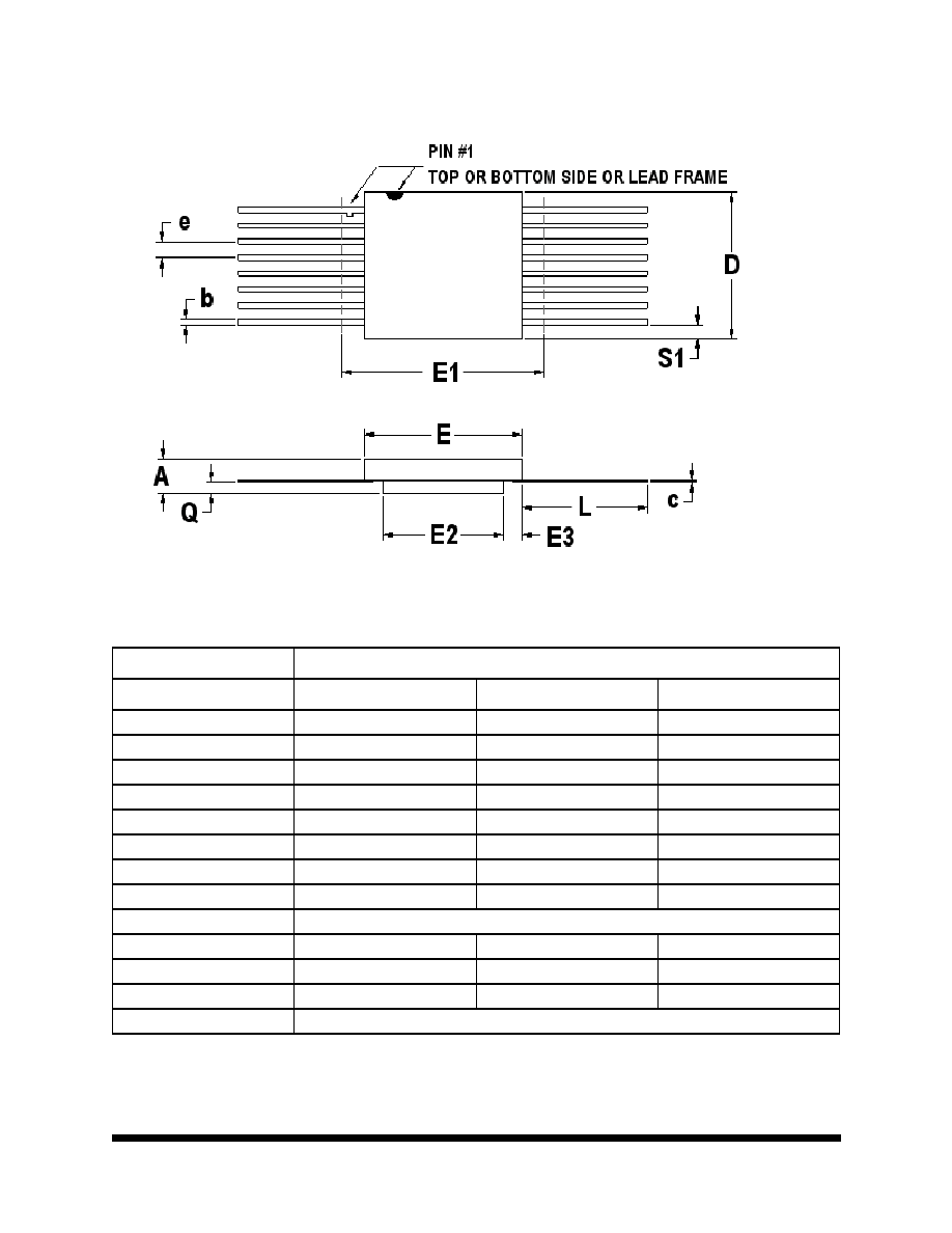
Note: All dimensions in inches.
16-P
IN
R
AK
-P
AK
Æ F
LAT
P
ACKAGE
SYMBOL
DIMENSION
M
IN
N
OM
M
AX
A
0.115
0.135
0.150
b
0.015
0.017
0.019
c
0.004
0.005
0.007
D
0.407
0.415
0.423
E
0.275
0.280
0.285
E1
--
--
0.500
E2
0.150
0.156
0.162
E3
0.030
0.062
--
e
0.050 BSC
L
0.325
0.335
0.345
Q
0.020
0.033
0.045
S1
0.005
0.024
0.045
N
16

OP400
Memory
9
All data sheets are subject to change without notice
©2001 Maxwell Technologies
All rights reserved.
Quad Low-Offset, Low-Power Operational Amplifier
09.12.02 REV 5
Important Notice:
These data sheets are created using the chip manufacturer's published specifications. Maxwell Technologies verifies
functionality by testing key parameters either by 100% testing, sample testing or characterization.
The specifications presented within these data sheets represent the latest and most accurate information available to
date. However, these specifications are subject to change without notice and Maxwell Technologies assumes no
responsibility for the use of this information.
Maxwell Technologies' products are not authorized for use as critical components in life support devices or systems
without express written approval from Maxwell Technologies.
Any claim against Maxwell Technologies must be made within 90 days from the date of shipment from Maxwell Tech-
nologies. Maxwell Technologies' liability shall be limited to replacement of defective parts.

OP400
Memory
10
All data sheets are subject to change without notice
©2001 Maxwell Technologies
All rights reserved.
Quad Low-Offset, Low-Power Operational Amplifier
09.12.02 REV 5
Product Ordering Options
Model Number
Feature
Option Details
OP400
RP
F
X
Screening Flow
Package
Radiation Feature
Base Product
Nomenclature
Monolithic
S = Maxwell Class S
B = Maxwell Class B
I = Industrial (testing @ -55∞C,
+25∞C, +125∞C)
E = Engineering (testing @ +25∞C)
F = Flat Pack
RP = R
AD
-P
AK
Æ package
Quad Low-Offset, Low Power
Operational Amplifier