 | –≠–ª–µ–∫—Ç—Ä–æ–Ω–Ω—ã–π –∫–æ–º–ø–æ–Ω–µ–Ω—Ç: MTI08 | –°–∫–∞—á–∞—Ç—å:  PDF PDF  ZIP ZIP |
REVISIONS
NO
VERSION
APPROVED
The information disclosed herein was originated by and is the
property of MAZeT. MAZeT reserves all patent, proprietary, design,
use, sales, manufacturing an reproduction rights thereto. Product
names used in this publication are for identification purposes only
and may be trademark of their respective companies.
1
V 1.5
2003-07-07
Approvals
Date
MAZeT GmbH
Compiled:
2003-07-07
Checked:
2003-07-07
Status: valid
MAZeT GmbH Sales
Gˆschwitzer Straþe 32
07745 JENA / GERMANY
Phone: +49 3641 2809-0
Fax: +49 3641 2809-12
E-Mail: sales@MAZeT.de
Url: http://www.MAZeT.de
Released:
2003-07-07
DOC. NO: DB-99-072e
Page 1 of 10
Data Sheet
MTI04Bx / MTI08Bx
MULTI-CHANNEL PROGRAMMABLE GAIN
TRANSIMPEDANCE AMPLIFIER
Table of contents
1.
GENERAL DESCRIPTION
2
2.
BLOCK DIAGRAM
2
3.
DESCRIPTION OF INTERFACE
3
3.1
Pinning
3
3.2
Adjustment Of Transimpedance
3
4.
DESCRIPTION OF FUNCTION
3
5.
ELECTRICAL CHARACTERISTICS
3
5.1
Absolute Maximum Ratings
3
5.2
Operating Conditions
4
5.3
AC/DC-Characteristics
4
5.3.1
Offset Voltage At Input INX
5
5.3.2
Leakage Current At Input INX
6
5.3.3
DC-Transfer-Curves
7
6.
PACKAGES
8
6.1
Shape and Dimensions
8
6.2
Pin-Configuration
8
7.
APPLICATIONS
9
7.1
Example For Position Measurement
9
7.2
Connection Of A Colour Sensor
9
8.
ORDERING INFORMATION
10
9.
CONTACT
10
REVISIONS
NO
VERSION
APPROVED
1
V 1.5
2003-07-07
The information in this publication is believed to be accurate in all respects at the time
of publication. MAZeT reserves the right to make changes in its products without notice
in order to improve design or performance characteristics.
DOC. NO:
DB-99-072e
Page 2 of 10
DATA SHEET MTI04Bx / MTI08Bx
1.
GENERAL DESCRIPTION
The MTI-devices are a family of integrated circuits of programmable gain
transimpedance amplifiers with different numbers of channels (4 or 8).
The MTI-devices are mainly used for signal conditioning of sensors with current
outputs. They are especially suitable for connection of photodiodes of array and row
sensors.
The possibility to adjust the transimpedance in 3 stages is a special feature.
The adjustment is made by programming two pins and is valid for all channels together.
The device packages are optimized for COB-mounting.
2.
BLOCK DIAGRAM
Rf
Cc
SW1 SW2
IN1
VREF
OUT1
OPAMP 1
-
+
Rf
Cc
INX
OUTX
OPAMP X
-
+
MTI
VDD GND
50k
W
- 150k
W
GND
REVISIONS
NO
VERSION
APPROVED
1
V 1.5
2003-07-07
The information in this publication is believed to be accurate in all respects at the time
of publication. MAZeT reserves the right to make changes in its products without notice
in order to improve design or performance characteristics.
DOC. NO:
DB-99-072e
Page 3 of 10
DATA SHEET MTI04Bx / MTI08Bx
3.
DESCRIPTION OF INTERFACE
3.1
Pinning
signal name
Typ.
a/d
a
function
VDD
input
a/d
power supply
GND
input
a/d
power supply
SW1
input
d
input 1 for adjustment of transimpedance of MTI-
amplifier (pull down)
SW2
input
d
input 2 for adjustment of transimpedance of MTI-
amplifier (pull down)
INX
input
a
analog current input of amplifier X
OUTX
output
a
analog voltage output of amplifier X
a.) analog or digital
3.2
Adjustment Of Transimped ance
settings of digital inputs
SW1
SW2
transimpedance Rf
GND
VDD
5MW ≠ stage 1
VDD
GND
500kW ≠ stage 2
GND
GND
25kW
a
≠ stage 3
VDD
VDD
not used
a.) default by pull down
4.
DESCRIPTION OF FUNCTION
The MTI-devices are programmable gain transimpedance amplifiers with different
numbers of channels (MTI04 ≠ 4 channels; MTI08 ≠ 8 channels). There is one
transimpedance amplifier per channel between a current input INX and a voltage output
OUTX. Its transimpedance is selectable in 3 stages. This adjustment can be effected by
setting of digital inputs SW1 and SW2 and is valid for all channels simultaneously
(headline 3.2). The inputs SW1 and SW2 are pulled down with a resistor for a default
feedback resistor of 25k.
The second input of all transimpedance amplifiers is used for a common supply by a
reference voltage necessarily fed in through the pin VREF.
All channels are compensated for an external input capacitance of the photo-sensor of
typical 20pF.
The power supply for the MTI-devices is typical 5V between VDD and GND.
5.
ELECTRICAL CHARACTERISTICS
5.1
Absolute Maximum Rating s
Violations of absolute maximum ratings are not allowed under any circumstances.
All voltages are referenced to VSS = 0V.
parameter
name
min.
max.
unit
power supply
VDD
0,3
7,0
V
input and output voltages
Þ IC-pinning
0,3
VDD 0,3
V
power dissipation
P
OP
0,1
W
operating temperature
T
OP
85
∞C
storage temperature
T
STG
55
155
∞C
REVISIONS
NO
VERSION
APPROVED
1
V 1.5
2003-07-07
The information in this publication is believed to be accurate in all respects at the time
of publication. MAZeT reserves the right to make changes in its products without notice
in order to improve design or performance characteristics.
DOC. NO:
DB-99-072e
Page 4 of 10
DATA SHEET MTI04Bx / MTI08Bx
5.2
Operating Conditions
All voltages are referenced to VSS = 0V.
parameter
name
min.
typ.
max.
unit
condition
supply voltage
VDD
4,5
5
5,5
V
Bias current MTI04
I(VDD)
3
4
mA
27∞C
Bias current MTI08
I(VDD)
12
16
mA
27∞C
operating temperature
T
OP
27
85
∞C
input high level
V
IH
2,0
VDD+0,3
V
input low level
V
IL
0,3
0,8
V
reference voltage
VREF
1
2,5
4
V
5.3
AC/DC-Characteristics
Unless otherwise specified the data in this table is valid for T
OP
= 27∞C and VDD = 5V.
parameter
name
min.
typ.
max.
unit
condition
0,1
µA
stage 1
1
µA
stage 2
input current
INX
20
µA
stage 3
4000
5000
6000
kW
stage 1
400
500
600
kW
stage 2
feedback resistor
Rf
20
25
30
kW
stage 3
25
kHz
stage 1
70
kHz
stage 2
signal frequency at input
f
3dB
500
kHz
stage 3
temperature coefficient of
the feedback resistor
TC
Rf
3500
ppm/K
input offset voltage
V
OFF
8
mV
T
OP
= 85∞C
input leakage current
I
LEAK
500
pA
T
OP
= 85∞C
capacitive load at OUTX
C
LOAD
50
pF
I
LOAD
= 0,5mA
pull down resistor at SW1
and SW2
R
PDSW
50
k
input capacitance of
external connected photo-
sensors
C
DIODE
20
pF
per input
REVISIONS
NO
VERSION
APPROVED
1
V 1.5
2003-07-07
The information in this publication is believed to be accurate in all respects at the time
of publication. MAZeT reserves the right to make changes in its products without notice
in order to improve design or performance characteristics.
DOC. NO:
DB-99-072e
Page 5 of 10
DATA SHEET MTI04Bx / MTI08Bx
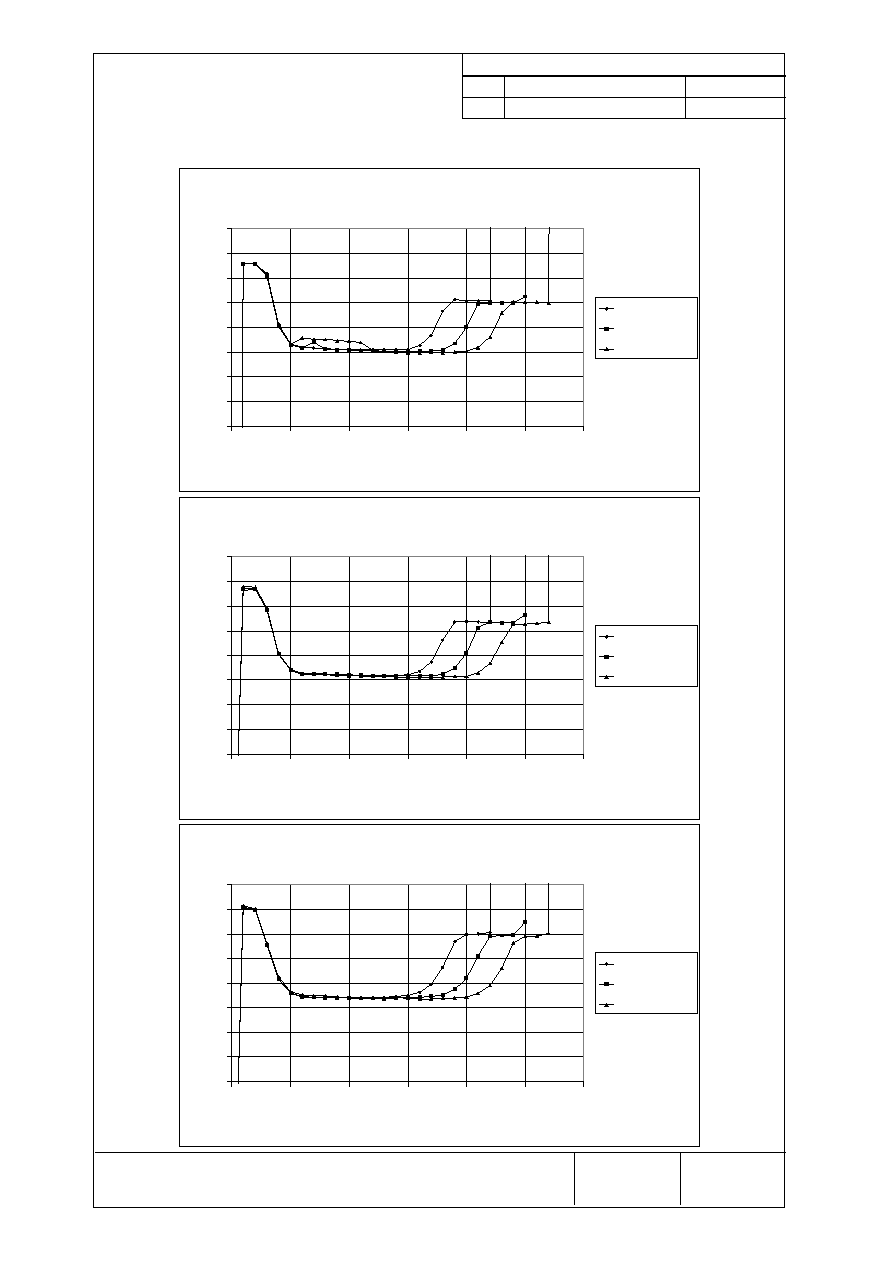
5.3.1
Offset Voltage At Input INX
Offset Voltage Voff = f(VREF) -- Temp = 0∞C
0
1
2
3
4
5
6
7
8
0
1
2
3
4
5
6
VREF -- V
V
o
ff
--
m
V
VDD = 4.5V
VDD = 5.0V
VDD = 5.5V
Offset Voltage Voff = f(VREF) -- Temp = 27∞C
0
1
2
3
4
5
6
7
8
0
1
2
3
4
5
6
VREF -- V
V
o
ff
--
m
V
VDD = 4.5V
VDD = 5.0V
VDD = 5.5V
Offset Voltage Voff = f(VREF) -- Temp = 85∞C
0
1
2
3
4
5
6
7
8
0
1
2
3
4
5
6
VREF -- V
V
o
ff
--
m
V
VDD = 4.5V
VDD = 5.0V
VDD = 5.5V