©
Macroblock, Inc. 2003
Floor 6-4, No. 18, Pu-Ting Rd., Hsinchu, Taiwan 30077, ROC.
TEL: +886-3-579-0068, FAX: +886-3-579-7534 E-mail:
info@mblock.com.tw
- 1 -
Macroblock
Preliminary Datasheet
MBI1008
LED Backlight Driver
Typical Application Circuit
General Description
MBI1008 is a CMOS constant current driver that
provides four regulated current sources. It is
designed to drive LEDs with matched currents
(within 5 %) to produce balanced light sources for
backlights.
MBI1008 is simple and easy to use. It accepts an
input voltage range from 2.7V to 8V and maintains
a constant current determined by an external
resistor, R1. Neither a capacitor, an inductor, nor
Schottky diode is needed. MBI1008 delivers up to
25mA of load current. In addition, customers can
get very high efficiency (up to 92%) by well
matching V
LED
input supply voltage and LED
forward voltages, Vf.
MBI1008 features low cost, high efficiency, easy
to use, and space-saving 6-pin SOT26 package
for applications that need uniform LEDs
illumination.
Features
n
4 constant-current output channels
n
High efficiency, up to 92%
n
Adjustable output current :15-25 mA
n
Very small size
≠
neither an inductor,
a
capacitor nor Schottky diode is
needed.
n
Small 6-pin SOT26 package
Applications
n
LED Backlight
n
Cellular Phones
n
PDAs
n
Digital Cameras
n
Portable MP3 Players
n
Pagers
V
LED
GND
R
SET
5
6 4 3 1
OUT0 OUT1 OUT2 OUT3
I
OUT
R1
3.8 K
2
V
OUT
I
SET
4.5V
Neither a capacitor, an inductor
nor Schottky diode is needed.
MBI1008
February, 2003, V1.2
- 2 -
LED Backlight Driver
Pin Description
Electrical Characteristics
(Ta = 25
∞
C
,
unless otherwise noted)
PARAMETER
SYMBOL
CONDITIONS
MIN
TYP
MAX
UNITS
Output Voltage
V
OUT
Current matching between
any two outputs less than 5
%
0.5
-
1.6
V
I
OUT
= 15mA
-
1.11
-
I
OUT
= 20mA
-
1.17
-
R
SET
Pin Voltage
V
RSET
I
OUT
= 25mA
-
1.22
-
V
Output Current
I
OUT
Input Voltage V
LED
= 4.5V,
R1= 3.8K
19.5
20.0
20.5
mA
Efficiency
Input Voltage V
LED
= 7.8V,
V
OUT
= 0.6V
-
92
-
%
Output Current
vs.Temperature
Variation
I
OUT
= 20 mA
0.0625
mA/
∞
C
Absolute Maximum Ratings
V
OUT
Voltage ...................................................... 8V
V
RSET
Voltage .................................................... 8V
I
LED
Current ................................................. 60 mA
Junction Temperature ................................. 125
∞
C
Operating Temperature Range ......
≠
20
∞
C to 85
∞
C
Storage Temperature Range .......
≠
65
∞
C to 150
∞
C
Package/Order Information
ORDER PART
NUMBER
MBI1008
PACKAGE
6-LEAD SOT26
OUT3
1
2
3
4
5
6
GND
OUT2
OUT1
R
SET
OUT0
1
0
0
8
Z
X
X
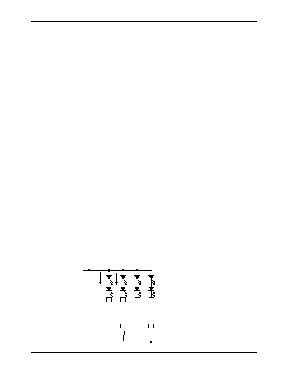
OUT3 (Pin 1):
Current output Pin. LED
'
s cathode
is connected to it.
GND (Pin 2):
Ground Pin. Tie this pin directly to
local ground plane.
OUT2 (Pin 3):
Current output Pin. LED
'
s cathode
is connected to it.
OUT1 (Pin 4):
Current output Pin. LED
'
s cathode
is connected to it.
R
SET
(Pin 5):
A resistor between this pin and V
LED
regulates the LED current flowing into the LED pin.
This pin is also used to provide LED dimming.
OUT0 (Pin 6):
Current output Pin. LED
'
s cathode
is connected to it.
MBI1008
February, 2003, V1.2
- 5 -
LED Backlight Driver
Application Information
Resistor Selection
R1 is used to regulate the LED current. For the best accuracy, a resistor with
±
1% precision
should be used.
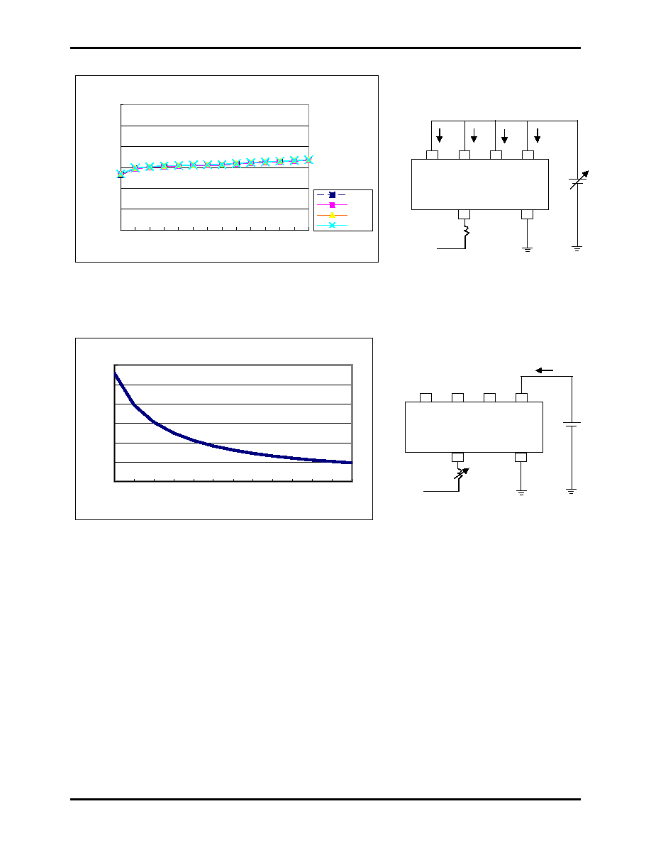
Regulating Output Current
LED current is regulated by a single resistor connected to the R
SET
pin (see Typical
Application Circuits). The voltage of R
SET
pin, V
RSET
, is internally regulated to around 1.17V,
which sets the current, I
SET
, flowing into this pin to equal to (V
LED
≠
V
RSET
) / R1. MBI1008
regulates the current into the LED pin, I
OUT
, to 22.85 times the value of I
SET
. A typical operating
characteristic of I
OUT
vs. R1 is shown (see Fig. 2). For other LED current values, use the
following equation to choose R1.
I
OUT
22.85 x (V
LED
≠
V
RSET
) / R1
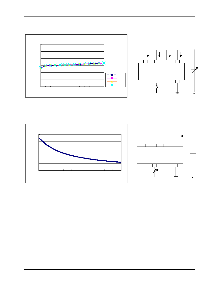
Efficiency Consideration
Except the output driver stage, the control parts of MBI1008 consume very little power (typical
value
8 mW). According to Fig. 1 and Fig. 5 (I
OUT
vs. V
OUT
), when V
OUT
is between 0.5V to
1.6V, the variations of I
OUT
would be within 5
. Moreover, V
OUT
= V
LED
- Vf , and thus V
LED
should be high enough to let V
OUT
be between 0.5V to 1.6V. On the other hand, the power
efficiency can be estimated as (V
LED
- V
OUT
) / V
LED
; thus ensuring to get higher efficiency, V
LED
should be as low as possible.
The following example shows how to achieve high power efficiency. (see Fig. 5).
For white LEDs, the forward voltage, Vf, ranges from 3.0V to 4.0V.
If
Vf1 + Vf2 = 7.2 V
V
LED
= Vf1 + Vf2 + V
OUT
= 7.8V, (let V
OUT
= 0.6V)
then
Efficiency = (V
LED
- V
OUT
) / V
LED
= 7.2V / 7.8V = 92.3%
Therefore, a proper design of V
LED
is strongly recommended in order to always let V
OUT
be its
minimum specification value, 0.6V, that is the key to get the high efficiency.
GND
2
R
SET
5
6 4 3 1
OUT0 OUT1 OUT2
OUT3
V
LED
I
OUT
R1
Vf1
Vf2
V
OUT
Fig. 5