©
Macroblock, Inc. 2003
Floor 6-4, No. 18, Pu-Ting Rd., Hsinchu, Taiwan 30077, ROC.
TEL: +886-3-579-0068, FAX: +886-3-579-7534 E-mail:
info@mblock.com.tw
- 1 -
Macroblock
Preliminary Datasheet
MBI5001
8-bit Constant Current LED Driver
GND
SDI
CLK
/LE
OUT0
OUT1
OUT2
OUT3
OUT4
OUT5
OUT6
OUT7
/OE
SDO
R-EXT
VDD
1
2
3
4
5
6
7
8
9
10
11
12
13
14
15
16
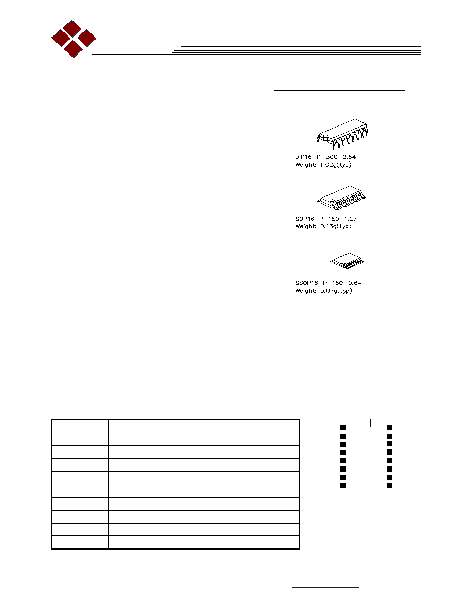
Terminal Description
PIN NO.
PIN NAME
FUNCTION
1
GND
GND terminal
2
SDI
Serial data input terminal
3
CLK
Clock input terminal
4
/LE
Latch input terminal
5-12
OUT0-7
Output terminal
13
/OE
Output enable input terminal
14
SDO
Serial data out terminal
15
R-EXT
Constant current programming
16
VDD
5V supply voltage terminal
M B I5 0 0 1 C P
M B I5 0 0 1 C D
M B I5 0 0 1 C N
Features
∑
8 constant-current output channels
∑
Output current adjustable through an external resistor
∑
Serial data in/parallel data out
∑
Output current: 5-90 mA
∑
20 MHz clock frequency
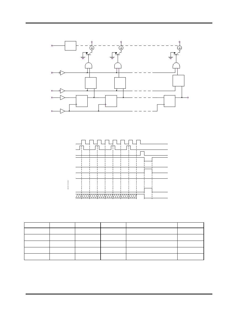
Product Description
MBI5001, utilizing the most advanced Si technology, is
targeted for LED panel display. MBI5001 contains
CMOS shift registers and latch functions converting
serial input data into parallel output format. At the output
stage, eight regulated current sources were designed to
provide 5-90 mA constant current for driving LEDs.
MBI5001 provides users with great flexibility and device performance while using the
MBI5001 in their LED panel system design. Users may adjust the output current of the
MBI5001 through an external resistor, Rext, which gives users flexibility in controlling the
light intensity of LEDs. MBI5001 guarantees to endure maximum 17V at the output port,
allowing users to connect more LEDs in series. The high clock frequency, 20 MHz, also
satisfies the system requirement of high volume data transmission.
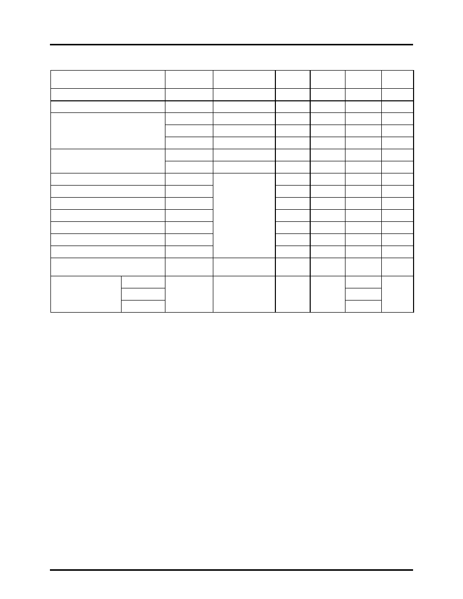
Pin Description
MBI5001
8-bit Constant Current LED Driver
February 2003, V1.2
- 3 -
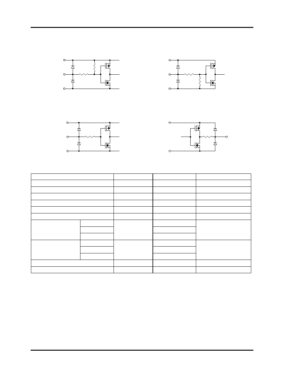
Equivalent Circuit of Inputs and Outputs:
VDD
VDD
VDD
VDD
GND
GND
GND
GND
/OE
/LE
CLK, SDI
SDO
8th LATCH
DATA
1. /OE terminal
2. /LE terminal
3. CLK, SDI terminal
4. SDO terminal
Maximum Ratings
CHARACTER
SYMBOL
RATING
UNIT
Supply Voltage
V
DD
0~+7.0
V
Output Voltage
V
CE
-0.5~+17.0
V
Output Current
I
OUT
+90
mA
Input Voltage
V
IN
-0.4~V
DD
+0.4
V
GND Terminal Current
I
GND
720
mA
Clock Frequency
F
CLK
20
MHZ
CN
≠
type
1.64
CD
≠
type
1.06
Power Dissipation
(ON PCB, Ta=25 )
CP
≠
type
P
D
0.88
W
CN
≠
type
76
CD
≠
type
117
Thermal Resistance
(ON PCB, Ta=25 )
CP
≠
type
R
th(j-a)
141
∞
C/W
Operating Temperature
T
opr
-40~+85
∞
C
Storage Temperature
T
stg
-55~+150
∞
C
MBI5001
8-bit Constant Current LED Driver
February 2003, V1.2
- 5 -
Electrical Characteristics
CHARACTERISTIC
SYMBOL
CONDITION
MIN. TYP. MAX. UNIT
"
H
"
level
V
IH
-
0.7V
DD
-
V
DD
V
Input Voltage
"
L
"
level
V
IL
-
GND
-
0.3V
DD
Output Leakage Current
I
OH
V
OH
=17.0V
-
-
10
A
V
OL
I
OL
=+1.0mA
-
-
0.4
V
Output Voltage SERIAL-OUT
V
OH
I
OH
=-1.0mA
-
-
-
V
Output Current 1
I
OL1
V
CE
=0.8V
R
ext
=865
(include Skew)
-
40.0
-
mA
Current Skew
dI
OL1
IO = 40mA
V
CE
= 0.8V
R
ext
=865
-
±
1.5
±
6.0
%
Output Current 2
I
OL2
V
CE
=1.2V
R
ext
=330
(include Skew)
-
80.0
-
mA
Current Skew
dI
OL2
IO = 80mA
V
CE
= 1.2V
R
ext
=330
-
±
1.5
±
6.0
%
Pull-up Resistor
RIN(up)
-
150
300
600
K
Pull-down Resistor
RIN(down)
-
85
200
400
K
I
DD
(off) 1
R
ext
=OPEN OUT0~7=Off
-
0.1
1.0
I
DD
(off) 2
R
ext
=865
OUT0~7=Off
0.1
0.2
1.0
"
OFF
"
I
DD
(off) 3
R
ext
=330
OUT0~7=Off
0.1
0.2
1.0
I
DD
(on) 1
R
ext
=865
OUT0~7=On
7.0
12.0
18.0
Supply Current
"
ON
"
I
DD
(on) 2
R
ext
=330
OUT0~7=On
10.0
22.0
32.0
mA
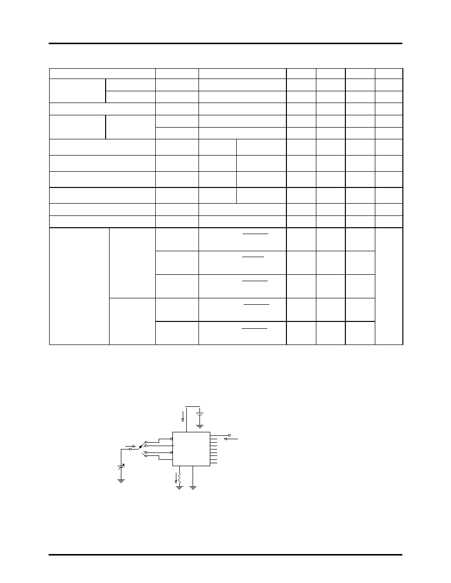
Test Circuit for Electrical Characteristics
, I
I
I
OL
I
R-EXT
GND
VDD
13
4
3
2
5
6
7
8
9
10
11
12
14
/OE
/LE
CLK
SDI
OUT0
OUT1
OUT2
OUT3
OUT4
OUT5
OUT6
OUT7
SDO
I
IL
IH
V
IL
, V
IH
REF
DD