©
Macroblock, Inc. 2003
Floor 6-4, No. 18, Pu-Ting Rd., Hsinchu, Taiwan 30077, ROC.
TEL: +886-3-579-0068, FAX: +886-3-579-7534 E-mail:
info@mblock.com.tw
- 1 -
Macroblock
Datasheet
MBI5016
16-bit Constant Current LED Sink Driver
MBI5016 provides users with great flexibility and device
performance while using MBI5016 in their LED panel
system design. Users may adjust the output current of
MBI5016 through an external resistor, R
ext
, which gives
users flexibility in controlling the light intensity of LEDs.
MBI5016 guarantees to endure 17V at the output port,
allowing users to connect more LEDs in series. The high
clock frequency, 20 MHz, also satisfies the system
requirement of high volume data transmission.
Features
l
16 constant-current output channels
l
Output current adjustable through an external resistor
l
Serial data in/parallel data out
l
Output current: 5-90 mA
l
20MHz clock frequency
Product Description
MBI5016, utilizing the most advanced silicon technology,
is targeted for LED panel display. MBI5016 contains
CMOS shift registers and latch functions, converting
serial input data into parallel output format. At the output
stage, sixteen regulated current sources, implemented in
Bipolar Junction Transistor, were designed to provide
5-90 mA constant current for driving LEDs.
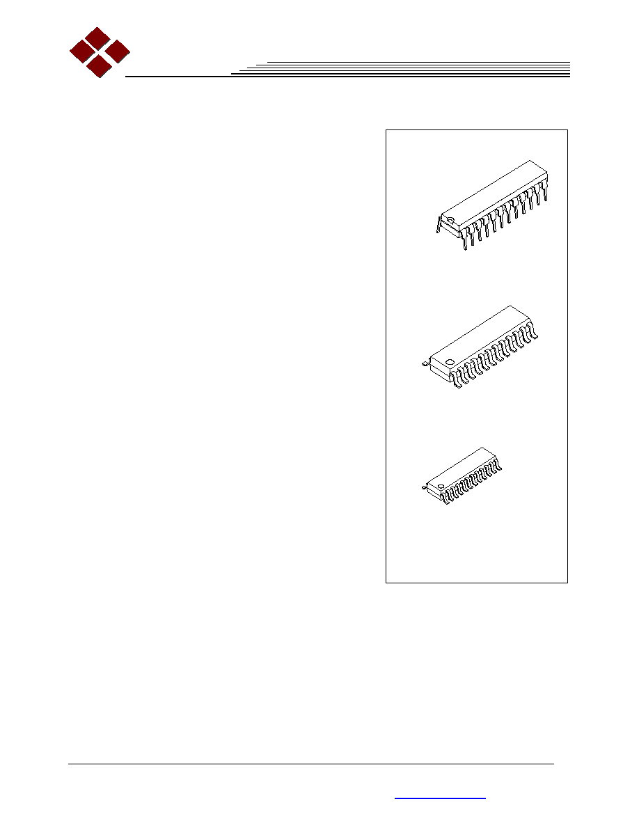
MBI5016CNS
MBI5016CNS
SDIP24-P-300-1.78
Weight: 1.11g(typ)
MBI5016CF
MBI5016CF
SOP24-P-300-1.00
Weight: 0.28g(typ)
MBI5016CP
SSOP24-P-150-0.64
Weight: 0.11g(typ)
MBI5016
16-bit Constant Current LED Sink Driver
May 2003, V1.6
- 2 -
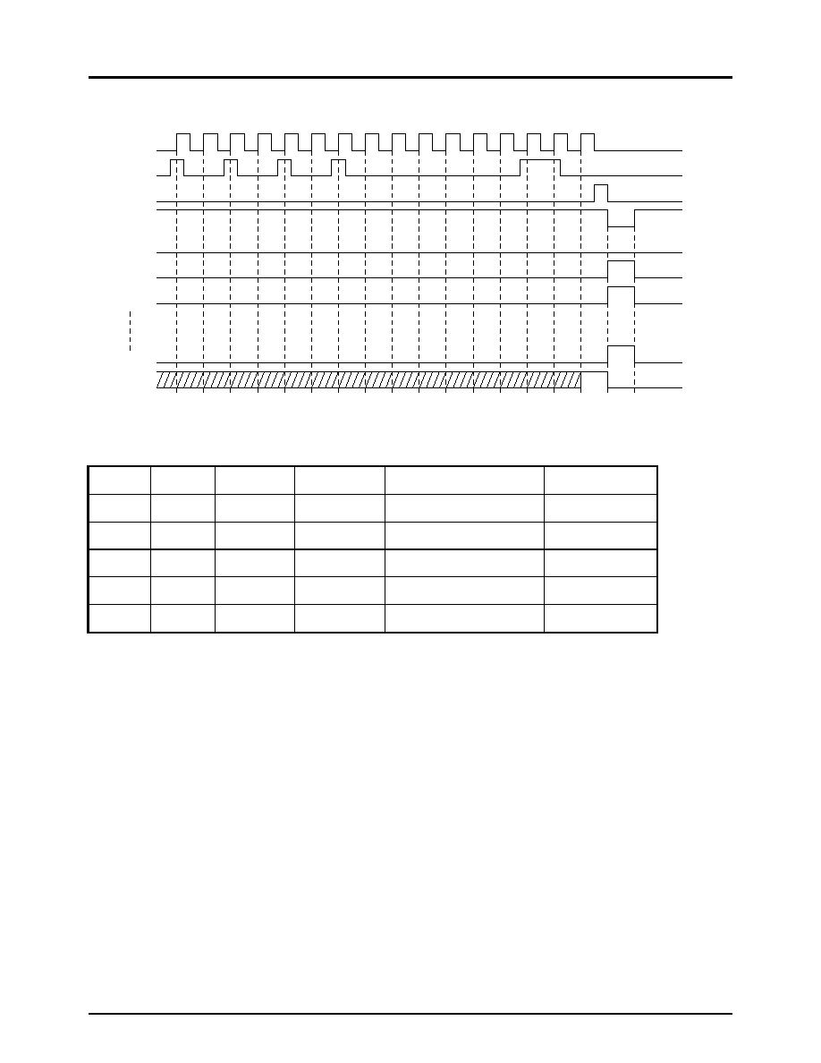
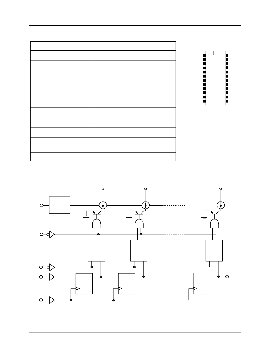
Terminal Description
Block Diagram
PIN NO.
PIN NAME
FUNCTION
1
GND
Ground terminal for control logic and current
sink
2
SDI
Serial-data input to the shift register
3
CLK
Clock input terminal for data shift on rising
edge
4
/LE
Data strobe input terminal
Serial data is transferred to the output latch
when /LE is high. The data is latched when
/LE goes low.
5~20
OUT0~OUT15 Constant current output terminals
21
/OE
Output enable terminal
When (active) low, the output drivers are
enabled; when high, all output drivers are
turned OFF (blanked).
22
SDO
Serial-data output to the following SDI of
next driver IC
23
R-EXT
Input terminal used to connect an external
resistor for setting up output current for all
output channels
24
VDD
5V supply voltage terminal
Pin Description
GND
SDI
CLK
/LE
OUT0
OUT1
OUT2
OUT3
OUT4
OUT5
OUT6
OUT7
/OE
SDO
R-EXT
VDD
1
2
3
4
5
6
7
8
9
10
11
12
13
14
15
16
OUT8
OUT9
OUT10
OUT11
OUT12
OUT13
OUT14
OUT15
17
18
19
20
21
22
23
24
OUT0
OUT1
OUT15
R-EXT
/OE
/LE
SDI
SDO
CK
CK
CK
I-REG.
Q
ST
Q
Q
CLK
D
ST D
ST D
D
D
Q
D
Q
Q
MBI5016
16-bit Constant Current LED Sink Driver
May 2003, V1.6
- 5 -
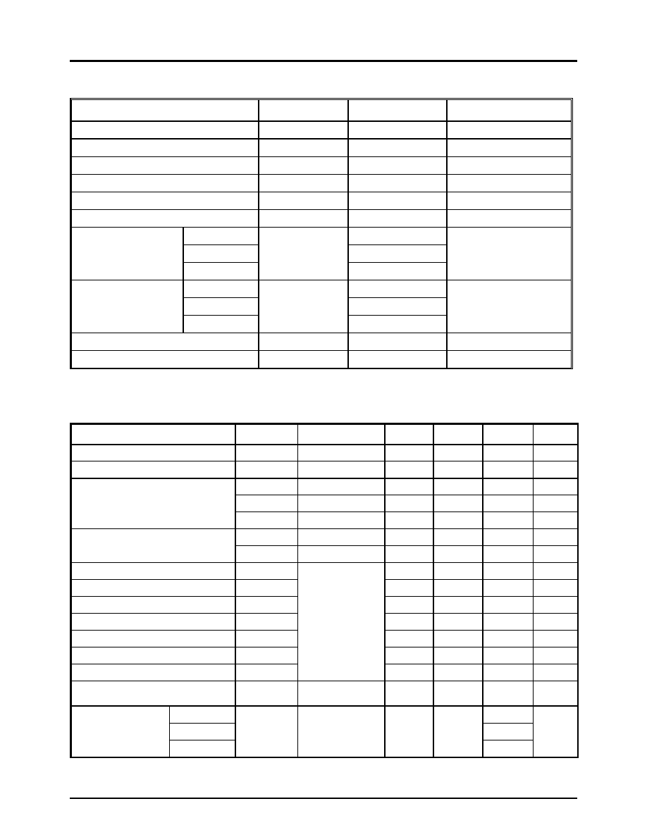
Maximum Ratings
CHARACTERISTIC
SYMBOL
RATING
UNIT
Supply Voltage
V
DD
0~+7.0
V
Output Voltage
V
CE
-0.5~+17.0
V
Output Current
I
OUT
+90
mA
Input Voltage
V
IN
-0.4~V
DD
+0.4
V
GND Terminal Current
I
GND
1440
mA
Clock Frequency
F
CLK
20
MHz
CNS
≠
type
1.52
CF
≠
type
1.30
Power Dissipation
(ON PCB, Ta=25 )
CP
≠
type
P
D
1.11
W
CNS
≠
type
82
CF
≠
type
96
Thermal Resistance
(ON PCB, Ta=25 )
CP
≠
type
R
th(j-a)
112
∞
C/W
Operating Temperature
T
opr
-40~+85
∞
C
Storage Temperature
T
stg
-55~+150
∞
C
Recommended Operating Condition
CHARACTERISTIC
SYMBOL
CONDITION
MIN.
TYP.
MAX.
UNIT
Supply Voltage
V
DD
-
4.5
5.0
5.5
V
Output Voltage
V
CE
-
-
-
17.0
V
I
OUT
DC Test Circuit
5
-
90
mA
I
OH
SDO
-
-
-1.0
mA
Output Current
I
OL
SDO
-
-
1.0
mA
V
IH
-
0.7V
DD
-
V
DD
+0.3
V
Input Voltage
V
IL
-
-0.3
-
0.3V
DD
V
/LE Pulse Width
t
w(L)
25
-
-
ns
CLK Pulse Width
t
w(CLK)
25
-
-
ns
/OE Pulse Width
t
w(OE)
400
-
-
ns
Setup Time for DATA
t
su(D)
20
-
-
ns
Hold Time for DATA
t
h(D)
15
-
-
ns
Setup Time for LATCH
t
su(L)
60
-
-
ns
Hold Time for LATCH
t
h(L)
V
DD
=4.5~5.5V
20
-
-
ns
Clock Frequency
F
CLK
Cascade
Operation
-
-
20.0
MHz
CNS
≠
type
0.79
CF
≠
type
0.67
Power Dissipation
CP
≠
type
P
D
Ta=85
∞
C
-
-
0.57
W