©
Macroblock, Inc. 2003
Floor 6-4, No.18, Pu-Ting Rd., Hsinchu, Taiwan 30077, ROC.
TEL: +886-3-579-0068, FAX: +886-3-579-7534 E-mail:
info@mblock.com.tw
- 1 -
Macroblock
Preliminary Datasheet
MBI5028
16-bit Constant Current LED Sink Driver
with Gain Control
Features
∑
16 constant-current output channels
∑
Output current adjustable through an external resistor
∑
Output current gain programmable for White Balance
∑
Constant output current range: 5-90 mA
∑
Excellent output current accuracy:
between channels:
±
3% (max.), and
between ICs:
±
6% (max.)
∑
Constant output current invariant to load voltage change
∑
Fast response of output current,
OE
(min.): 200 ns
∑
25MHz clock frequency
∑
Schmitt trigger input
∑
5V supply voltage
Current Accuracy
Between Channels
Between ICs
Conditions
<
±
3%
<
±
6%
I
OUT
= 10 mA ~ 60 mA
MBI5016CP
MBI5016CF
MBI5016CNS
MBI5028CNS
MBI5028CF
MBI5028CP

MBI5028 16-bit Constant Current LED Sink Driver with Gain Control
April 2003, V0.8-4
- 2 -
Product Description
MBI5028 succeeds MBI5026 and is designed for LED displays with Gain Control extension.
MBI5028 exploits PrecisionDrive
TM
technology to enhance its output characteristics. MBI5028
contains a serial buffer and data latches, which convert serial input data into parallel output
format. At MBI5028 output stage, sixteen regulated current ports are designed to provide
constant current sinks for driving LEDs within a wide range of Vf variations.
MBI5028 provides users with great flexibility and device performance while using MBI5028 in
their LED panel system design. Users may adjust the output current from 5 mA to 90 mA
through an external resistor R
ext
, which gives users flexibility in controlling the light intensity of
LEDs. MBI5028 guarantees to endure maximum 17V at the output port. The high clock
frequency, 25 MHz, also satisfies the system requirements of high volume data transmission.
MBI5028 also exploits Share-I-O
TM
technology and is backward compatible with MBI5026 in
both electrical characteristics and package aspect. To utilize the Current Adjust feature with
Share-I-O
TM
technology, users may not need to change the printed circuit board originally for
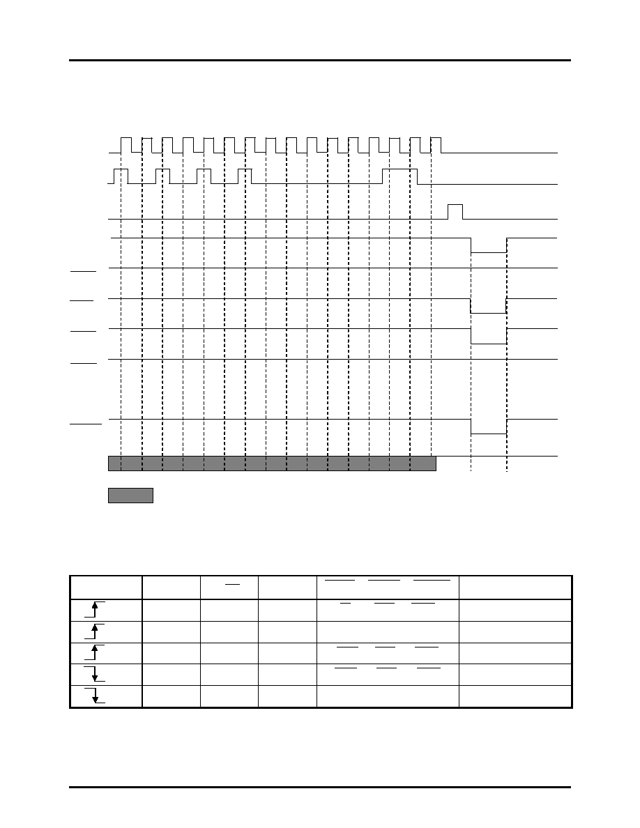
MBI5026. To enter a special function mode- Current Adjust mode, users just need to set a
sequence of signals on LE(CA1),
OE
(CA2) and CLK input pins. Normally, the output current
can be regulated only through an external resistor. In addition, in the Current Adjust mode, the
output current can be software-programmable by a system controller. The system controller
adjusts the output current by sending a 7-bit Current Adjust code to 16-bit Configuration Latch
through MBI5028 SDI pin. The code will be latched and effective to control the output current
regulator. A fine adjustment of the output current could be achieved by a gain ranging from 0.5
to 2 with 128 fine steps. By setting another sequence of signals on LE(CA1),
OE
(CA2) and
CLK input pins, MBI5028 may resume to a Normal mode and perform as MBI5026. The Shift
Register, with SDI, SDO, and CLK, carries the image data as usual.
A Share-I-O
TM
technique is specifically applied to MBI5028. By means of the Share-I-O
TM
technique, an additionally effective function, Current Gain, can be added to LED drivers,
however, without any extra pins. Thus, MBI5028 could be a drop-in replacement of MBI5026.
The printed circuit board originally designed for MBI5026 may be also applicable for MBI5028.
For MBI5028, the pin 4, LE(CA1), and the pin 21, OE (CA2), can be acted as different functions
as follows:
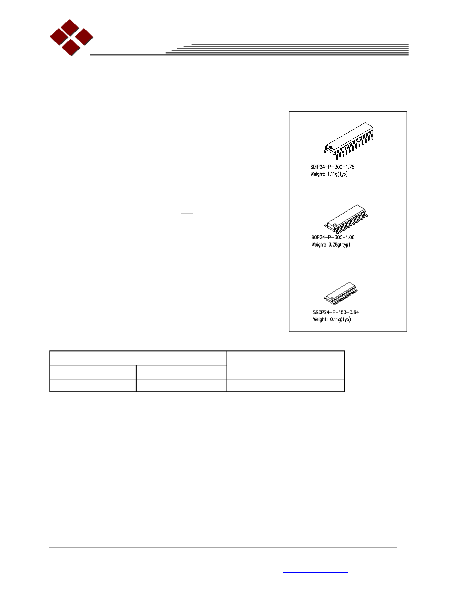
Pin
Device Name
MBI5028
Function Description of Pin 4
LE + Current Adjust (CA1)
Function Description of Pin 21
OE + Current Adjust (CA2)

MBI5028 16-bit Constant Current LED Sink Driver with Gain Control
April 2003, V0.8-4
- 3 -
GND
SDI
CLK
LE(CA1)
OUT7
OE(CA2)
SDO
R-EXT
VDD
1
2
3
4
5
6
7
8
9
10
11
12
13
14
15
16
17
18
19
20
21
22
23
24
OUT8
OUT6
OUT5
OUT4
OUT3
OUT2
OUT1
OUT0
OUT9
OUT10
OUT11
OUT12
OUT13
OUT14
OUT15
Block Diagram
Terminal Description
Pin No.
Pin Name
Function
1
GND
Ground terminal for control logic and current sink
2
SDI
Serial-data input to the Shift Register
3
CLK
Clock input terminal for data shift on rising edge
4
LE(CA1)
Data strobe input terminal
Serial data is transferred to the respective latch
when LE(CA1) is high. The data is latched when
LE(CA1) goes low.
Also, a control signal input for Current Adjust
mode (See Timing Diagram)
5~20
OUT0 ~ OUT15 Constant current output terminals
21
OE (CA2)
Output enable terminal
When (active) low, the output drivers are enabled;
when high, all output drivers are turned OFF
(blanked).
Also, a second control signal input for Current
Adjust mode (See Timing Diagram)
22
SDO
Serial-data output to the following SDI of next
driver IC
23
R-EXT
Input terminal used to connect an external resister
for setting up all output current
24
VDD
5V supply voltage terminal
Pin Configuration
LE(CA1)
16-bit Shift Register
16-bit Output Latch
16-bit Configuration Latch
I
O
Regulator
16-bit Output Driver
Control Logic
R-EXT
SDI
CLK
SDO
16
16
16
7
GND
VDD
OUT0
1
OUT
OUT14
OUT15
(CA2)
OE