
1
P/N:PM0730
REV. 0.1, FEB. 14, 2003
MX10F201FC
FEATURES OF MX10F201FC (80C51 with MTP memory and LCD)
- 80C51 CPU core
- 4.5 ~ 5.5V voltage range
- 2 to 16MHz clock frequency
- 16K bytes MTP memory for code memory
- 512 bytes internal data RAM
- Low power consumption
- Up to 16 digits LCD driver/controller
- Four 8 bit general purpose I/O ports
- Two standard 16-bit Timers
- On-chip Watch Dog Timer
- Two channel PWM outputs
- UART
- 8 interrupt sources
- 100 pin PQFP package
- Single clock or dual clock
- EMI compatibility
Features list
- 80C51 CPU core
- 4.5 ~ 5.5V operation voltage range
- 2 to 16MHz clock frequency
- 16K bytes MTP memory for code memory
- More than 100 times program/erase cycles
- More than 10 years data retention
- 512 bytes internal data RAM
- Low operation current
- Power saving modes
- User friendly power control for active mode current
- Idle mode
- Sleep mode
- Power down mode, can be wake up by external interrupts or RESET
- LCD driver/controller
- Max. 16-digits display at 1/4 duty LCD
- 1:1(static), 1:2, 1:3 or 1:4 selectable LCD multiplexing rate
- 4 backplane driver, 32 segment driver
- LCD directly drive capability with display memory
- VLCD to control LCD driving voltage, (VLCD-VSS)
- 4x8 general purpose I/O ports
- Provide software I
2
C capability
- Two standard 16-bit Timers (Timer 0,1)
- On-chip Watch Dog Timer (WDT)
- Two channel PWM outputs
- UART
- Up to 8 interrupt sources and 8 interrupt vectors
- 4 external sources
- 4 internal sources(Timer0,Timer1,watch Timer and UART)
- 100 pin PQFP package
- Single clock or dual clock
- single clock mode : 2~16MHz system clock for CPU,Timer0/1,WDT,UART and LCD
- dual clock mode : 2~16MHz system clock for CPU,Timer0/1,WDT,UART; while 32.768KHz sub-system
clock for LCD and watch timer.
- system clock is either crystal or RC activated
- EMC(Electro-Magnetic Compatibility) improved
2
P/N:PM0730
REV. 0.1, FEB. 14, 2003
MX10F201FC
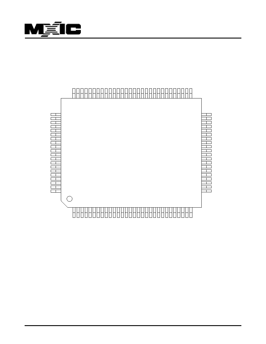
PINNING
NC
NC
P26
P25
P24
P23
P22
P21
P20
NC
NC
NC
P37/INT3
P36/INT2
P35/T1
P34/T0
P33/INT1
P32/INT0
P31/TxD
P30/RxD
NC
NC
S5
S6
S7
S8
S9
S10
S11
S12
S13
S14
S15
S16
S17
S18
S19
S20
S21
S22
NC
S23
S24
S25
S26
S27
S28
S29
S30
S31
VLCD
NC
VSS
NC
RESET
XT
AL1
XT
AL2
VDD
NC
VSS
RCP
P00
P01
P02
P03
P04
P05
P06
P07
NC
NC
S4
S3
S2
S1
S0
BP3
BP2
BP1
BP0
NC
VDD
NC
VSS
XT
AL3
XT
AL4
NC
P17
P16
P15/PWM1
P14/PWM0
P13
P12
P11
P10
NC
VPP
NC
NC
P27
1
2
3
4
5
6
7
8
9
10
11
12
13
14
15
16
17
18
19
20
21
22
23
24
25
26
27
28
29
30
50
49
48
47
46
45
44
43
42
41
40
39
38
37
36
35
34
33
32
31
80
79
78
77
76
75
74
73
72
71
70
69
68
67
66
65
64
63
62
61
60
59
58
57
56
55
54
53
52
51
81
82
83
84
85
86
87
88
89
90
91
92
93
94
95
96
97
98
99
100
MX10F201FC
Fig.1 Pinning

3
P/N:PM0730
REV. 0.1, FEB. 14, 2003
MX10F201FC
Table. 1 Pin Description
I/O SYMBOL
PIN \QFP 100
DESCRIPTION
O
BP0-BP3
71~74
Backplane drive output line 0 to 3.
O
S00-S31
75-79,83-100,
Segment drive output line 0 to 31.
2-10
I/O P00-P07
22-29
Port:8-bit open drain bidirectional I/O Port
I/O P20-P27
42-48,51
Port: 8-bit quasi-bidirectional I/O Port with
internal pull-up
I/O P10-P17
56-63
Quasi-bidirectional I/O lines
P14
also for PWM channel 0
P15
also for PWM channel 1
I/O P30-P37
31-38
Quasi-bidirectional I/O lines
P30
31
also for UART Receive
P31
32
also for UART Transmit
P32-P33,
also for external interrupt 0-3
P36-P37
P34
also for Timer0 external input
P35
also for Timer1 external input
I
RESET
15
reset input
I
VDD
18,69
Positive power supply
I
VSS
13,20,67
Ground
I
XTAL1
16
XTAL connection input
O
XTAL2
17
XTAL connection output
I
XTAL3
66
32.768KHz, XTAL input
O
XTAL4
65
32.768KHz, XTAL output
I
RCP
21
RC oscillator resistor connection input
I
TEST/VPP 54
Supply 12V power for programming / erasing
I
VLCD
11
LCD driver power supply
Note:
1. To avoid a 'Latch-up' effect at power-on , the voltage on any pin (at any time )must not be higher than V
DD
+0.5 V
or lower Vss-0.5V respectively
2. The generation or use of a Port 3 pin as an alternative function is carried out automatically by the associated
Special Function Register (SFR) bit is properly written .

4
P/N:PM0730
REV. 0.1, FEB. 14, 2003
MX10F201FC
Fig.3 LCD Driver Block Diagram
Fig.2 Block Diagram
T0 T1 INT0/1/2/3
3
3
XTAL1
XTAL2
RESET
T0/T1
Two 16-bit
Counter
CPU
Program
Memory
16KB
Data
Memory
512x8
RAM
PWM
Serial
Port
8-bit internal Bus
Parallel I/O
Ports
LCD Unit
T D R D
S00-S31 BP3 BP2 BP1 BP0
8
8
8
8
Watch
Dog
Timer
P0 P1 P2 P3
Alternative Function of Port3
3
3 3
VPP VDD VLCD VSS PWM0 PWM1
3
3
3
3
LCD Segment
Display Register
LCD Freq
LCD Duty
BIAS
ENLCD
Div ider
Timing/Duty
Control,
Voltage
Selector
LCD
BIAS
Gen.
Backplane Gen.
Segment Gen.
BP Driver
Seg. Driver
LCD Panel
SEG31 SEG30....SEG0
BP0
BP1
BP2
BP3
LCON
Ext.CLK
LCD_CL K
8
Internal Bus
BP3_SEG[31:0]
BP0_SEG[31:0]
4 BP_Output [1:0]
32 Seg_Output [1:0]
32
4
VLCD
VSS

5
P/N:PM0730
REV. 0.1, FEB. 14, 2003
MX10F201FC
FUNCTIONAL DESCTIPTION
General
The MX10F201FC is a stand-alone high-performance and low power microcontroller designed for use in many
applications which need code programmability.
The Flash EPROM offers customers to program the device themselves. This feature increases the flexibility in
many applications, not only in development stage, but also in mass production stage.
In addition to the 80C51 standard functions, the MX10F201FC provides a number of dedicated hardware functions.
MX10F201FC is a control-oriented CPU with on-chip program and data memory. It can execute program with internal
memory up to 16k bytes. MX10F201FC has four software selectable modes of reduced activity for power reduction :
active power control, idle, sleep, and Power-down. The idle mode freezes the CPU while allowing the RAM, Timers,
serial ports, interrupt system and other peripherals to continue functioning. The Power-down mode saves the RAM
contents but freezes the oscillator causing all other chip functions to be inoperative. Power-down mode can be
terminated by an external reset ,and in addition , by either of the four external interrupts. The sleep mode behaves like
power down mode, but with LCD and oscillator still turning on. And sleep mode can be terminated as the power down
mode does.
Instruction Set Execution
The MX10F201FC uses the powerful instruction set of the 80C51. Additional SFRs are incorporated to control the
on-chip peripherals. The instruction set consists of 49 single-byte, 46 two-bytes, and 16 three-bytes instructions.
When using a 16MHz oscillator, 64 instructions execute in 750 ns and 45 instructions execute in 1.5 us. Multiply and
divide instructions execute in 3 us.
MEMORY ORGANIZATION
The Central Processing Unit (CPU) manipulates operands in three memory spaces; these are the 256 bytes
internal data memory (RAM), 256 byte auxiliary data memory (AUX-RAM) and 16k byte internal MTP program memory
(FEPROM).
Program Memory
The program memory address space of the MX10F201FC comprises an internal and an external memory space.
The MX10F201FC has 16k byte of program memory on-chip.
Program Protection
If the user choose to set security lock in MTP memory, the program content is protected from reading out of chip.
Internal Data Memory
The internal data memory is divided into three physically separated parts: 256 byte of RAM, 256 bytes of AUX-
RAM, and 128 bytes special function register area (SFR). These parts can be addressed as follows (see Fig.4 and
Table. 2)
- RAM 0 to 127 can be addressed directly and indirectly as in the 80C51. Address pointers are R0 and R1 of
the selected register bank.
- RAM 128 to 255 can only be addressed indirectly . Address pointers are R0 and R1 of the selected register
bank.
- AUX-RAM 0 to 255 is indirectly addressable as the external data memory locations 0 to 255 with the MOVX
instructions. Address pointers are R0 and R1 of the selected register bank and DPTR. When executing from
internal program memory, an access to AUX_RAM 0 to 255 will not affect the ports P0,P2,P3.6 and P3.7.
SFRs can only be addressed directly in the address range from 128 to 255.