1
P/N:PM0723
REV. 1.0, JUL. 13, 2000
MX98728EC
GMAC
SINGLE CHIP 10/100 FAST ETHERNET CONTROLLER
FOR GENERIC APPLICATION
1.0 Features
∑ 32 bits general purpose asynchronous bus architec-
ture up to 33Mhz for easy system application
∑ Single chip solution integrating 10/100 TP transceiver
to reduce overall cost
∑ Optional MII interface for external tranceiver.
∑ Fully compliant with the IEEE 802.3u spec.
∑ Supports 32/16 bits x1, x2, x4 burst read transfers
for the receive packet buffer
∑ Packet buffer access through an IO mapped port or
host DMA for a wide variety of bus applications
∑ Programmable bus integrity check timer and interrupt
assertion scheme
∑ Supports 16/8 bits packet buffer data width and 32/
16 bits host bus data width
∑ Separated TX and RX FIFOs to support the full du-
plex mode, independent TX and RX channel
∑ Rich on-chip registers to support a wide variety of
network management functions
∑ 1.6KB TX FIFO to support maximum network through-
put in the full duplex mode
∑ 16/8 bits SRAM interface of the packet buffer sup-
porting burst DMA for on-chip FIFOs
∑ Flexible packet buffer partition and addressing space
for up to 1MB
∑ NWAY autonegotiation function to automatically set
up network speed and protocol
∑ 3 loop back modes for system level diagnosis
∑ Supports 64 bits hash table for multicast addressing,
broadcast control.
∑ Optional EEPROM configuration, supports 1K bits and
4K bits EEPROM interface
∑ Supports software EEPROM interface for easy up-
grade of EEPROM contents
∑ 5V CMOS in an 160 PQFP package
1.1 Introduction
MX98728EC ( GMAC ) is a general purpose single chip
10/100 Fast Ethernet controller. With no glue logic or very
little extra logic, it can be used in a variety of system
applications through its host bus interface. Single chip
solution will help reduce system cost, not only on the IC
count but also on the board size. Full NWAY function
with 10/100 transceiver will ease the field installation.
Simply plug the chip in and it will connect itself with the
best protocol available.
A data cache is also used on the host bus to deliver the
32 /16 bits burst read on the host data port up to 4 data
transfers in a single cycle. Two hand shake signals to
communicate to the host bus interface during the data
port transfer are simple and fast for the system integra-
tor. An intelligent built-in SRAM bus arbiter will manage
all SRAM access requests from the host bus access,
the transmit local DMA and the receive local DMA.
The 16/8 bit SRAM interface with local DMAs help sys-
tem developers to optimize the performance. The be-
havior of these local DMAs can be easily adjusted by
the optional bits on the chip. (The term "packet buffer"
and "packet memory" are used interchangeably in this
document).
A programmable receive packet interrupt scheme using
a timer (RXINTT) and a packet counter (RXINTC) allows
system developers to adjust the interrupt traffic. The re-
ceive interrupt assertion timing is also programmable
for different system applications. A general purpose host
receive packet counter (HRPKTCNT) is also provided to
the host for the buffer management purpose.
Bus integrity check feature allows the system to recover
from a bus hang or an excessively long bus access.
BICT ( Bus integrity check timer ) can be programmed
to abort any bus access that runs abnormally long. Based
multicast and broadcast frame filtering is supported to
minimize the unnecessary network traffic.
MX98728EC is also equipped with the back-to-back
transmit capability which allows the software to fire as
many transmit packets as needed in a single command.
The receive FIFO also allows the back-to-back recep-
tion. Optional EEPROM can be used to store the MAC
ID and the other configuration information. All options
including MAC ID can be programmed through the host
interface.

5
P/N:PM0723
REV. 1.0, JUL. 13, 2000
MX98728EC
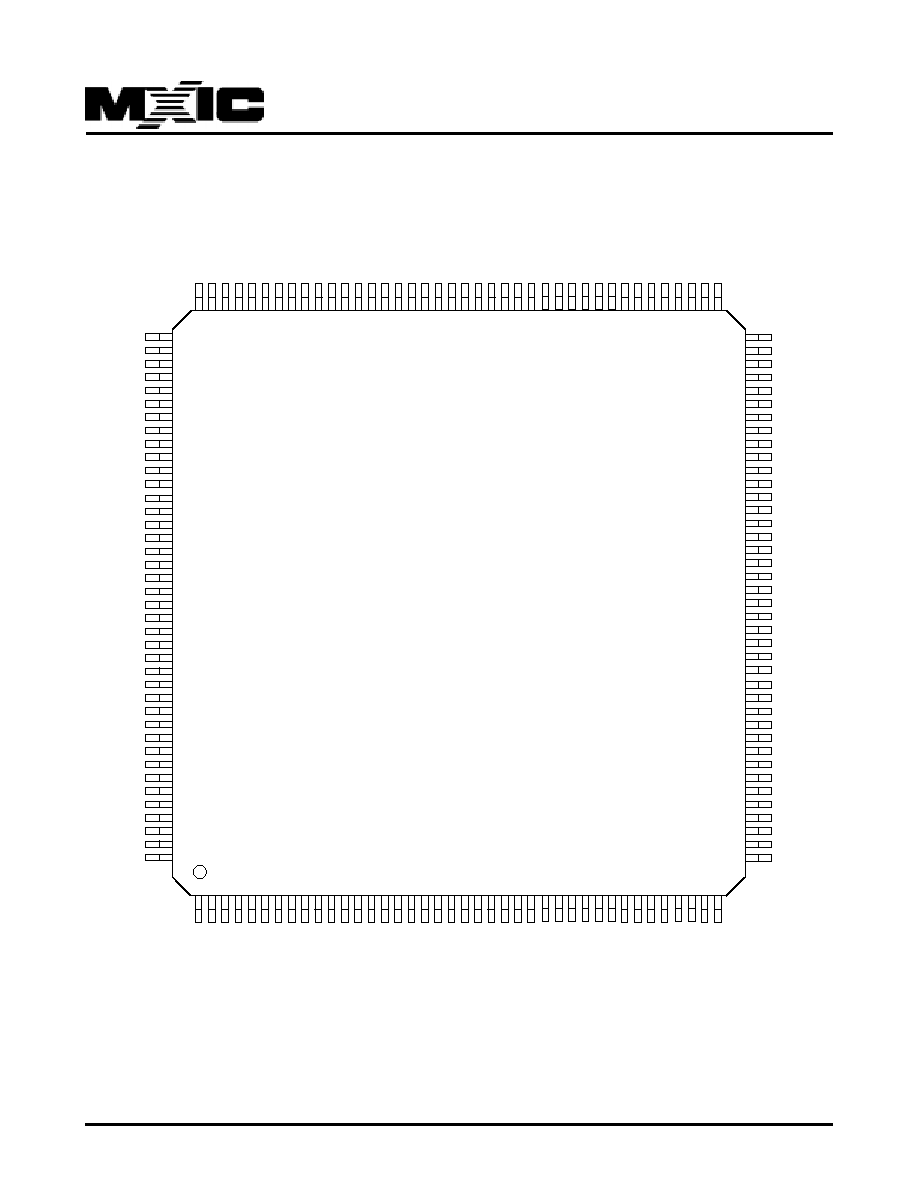
2.1 Pin Description: ( all internal pull-up is 168K ohm, pull-down is 70K ohm )
Host Bus Interface
PIN#
Pin Name
Type
Description
143
CLKIN
I, TTL
Not used, NC pin.
19-12,
D[31:0]
I/O, 4ma
Host Data Bit [31:0]:
101-103,
105-106,
108-114,
122-125,
92-97,
99, 100
117-120,
A[15:1]
I, 4ma
Host Bus Address Bit [15:1] : In 32 bit mode, H16_32=0,
126-129,
all host accesses are 32 bit wide. When H16_32=1, all
131-133,
host accesses are 16 bit wide. (Internal pull-up).
136,138-140
A11, A10, A9, A8 has other definition in MII mode.
126
A11(RXC)
I, TTL
Host Bus Address Bit11, when on-chip tranceiver is used,
it is used in A[15:1], when in MII mode, it is defined as
receive clock RXC (25MHz or 2.5MHz) When this pin is
used as address bit, it is internally grounded until Reg50.6
(A11A8EN bit) is set to enable decoding of this pin as
address bit.
127
A10(RXDV)
I,TTL
Host Bus Address Bit10, when on-chip tranceiver is used,
it is used in A[15:1], when in MII mode, it is defined as
receive data valid RXDV signal. When this pin is
used as address bit, it is internally grounded until Reg50.6
(A11A8EN bit) is set to enable decoding of this pin as
address bit.
128
A9(CRS)
I,TTL
Host Bus Address Bit9, when on-chip tranceiver is used,
it is used in A[15:1], when in MII mode, it is defined as
carrier same CRS signal. When this pin is
used as address bit, it is internally grounded until Reg50.6
(A11A8EN bit) is set to enable decoding of this pin as
address bit.
129
A8(COL)
I,TTL
Host Bus Address Bit8, when on-chip tranceiver is used,
it is used in A[15:1], when in MII mode, it is defined as
collision COL signal. When this pin is used as address
bit, it is internally grounded until Reg50.6 (A11A8EN bit)
is set to enable decoding of this pin as address bit.
141
NC
NC pin : Not connected.
137
SRDY
O, 4ma
Synchronous Ready : Active high for the write cycle to
indicate the data is secured and the cycle can be fin-
ished.