
MD1060
This specification are subject to be changed without notice. Any latest information please preview
http;//www.mdtic.com.tw
P. 1
2002/10 Ver. 1.5
1. General Description
This ROM-Based 8-bit micro-controller uses a fully
static CMOS technology process to achieve higher
speed and smaller size with the low power
consump-tion and high noise immunity. On chip
memory incl-udes 1K words of ROM, and 36 bytes of
static RAM.
2. Features
The followings are some of the features on the
hardware and software :
u
Fully COMS static design
u
8-bit data bus
u
On chip ROM size : 1.0 K words
u
Internal RAM size : 49 bytes
(36 general purpose registers, 13 special
registers)
u
37 single word instructions
u
14-bit instructions
u
8-level stacks
u
Operating voltage : 2.5 V ~ 6.5 V (PRD Disable)
u
4.5 V ~ 6.5 V (PRD Enable)
u
Operating frequency : DC ~ 20 MHz
u
The most fast execution time is 200 ns under
20 MHz in all single cycle instructions except
the branch instruction
u
Addressing modes include direct, indirect and
relative addressing modes
u
Power-on Reset
u
Power edge-detector Reset
u
Power range-detector Reset
u
Sleep Mode for power saving
u
3 interrupt sources:
-External INT pin
-TMR0 timer
-PortB<7:4> interrupt on change
u
4 types of oscillator can be selected by
programming option:
RC
Low cost RC oscillator
LFXT
Low frequency crystal oscillator
XTAL
Standard crystal oscillator
HFXT
High frequency crystal oscillator
u
8-bit real time clock/counter(RTCC) with 8-bit
programmable prescaler
u
On-chip RC oscillator based Watchdog
Timer(WDT)
u
13 I/O pins with their own independent
direction control
3. Applications
The application areas of this MD1060 range from
appliance motor control and high speed automotive
to low power remote transmitters/receivers, pointing
devices, and telecommunications processors, such
as Remote controller, small instruments, chargers,
toy, automobile and PC peripheral ... etc.
4. Pin Assignment
PA2 1
18 PA1
PA3 2
17 PA0
PA4/RTCC 3
16 OSC1
/MCLR 4
15 OSC2
V
ss
5
14 V
dd
PB0/INT 6
13 PB7
PB1 7
12 PB6
PB2 8
11 PB5
PB3 9
10 PB4

MD1060
This specification are subject to be changed without notice. Any latest information please preview
http;//www.mdtic.com.tw
P. 2
2002/10 Ver. 1.5
5. Pin Function Description
Pin Name
I/O
Function Description
PA0~PA3
I/O
Port A, TTL input level
PB0~PB7
I/O
Port B, TTL input level / PB0:External interrupt input ,
PB4~PB7:Interrupt on pin change
RTCC/PA4
I/O
Real Time Clock/Counter, Schmitt Trigger input levels
Open drain output
/MCLR
I
Master Clear, Schmitt Trigger input levels
OSC1
I
Oscillator Input
OSC2
O
Oscillator Output
V
dd
Power supply
V
ss
Ground
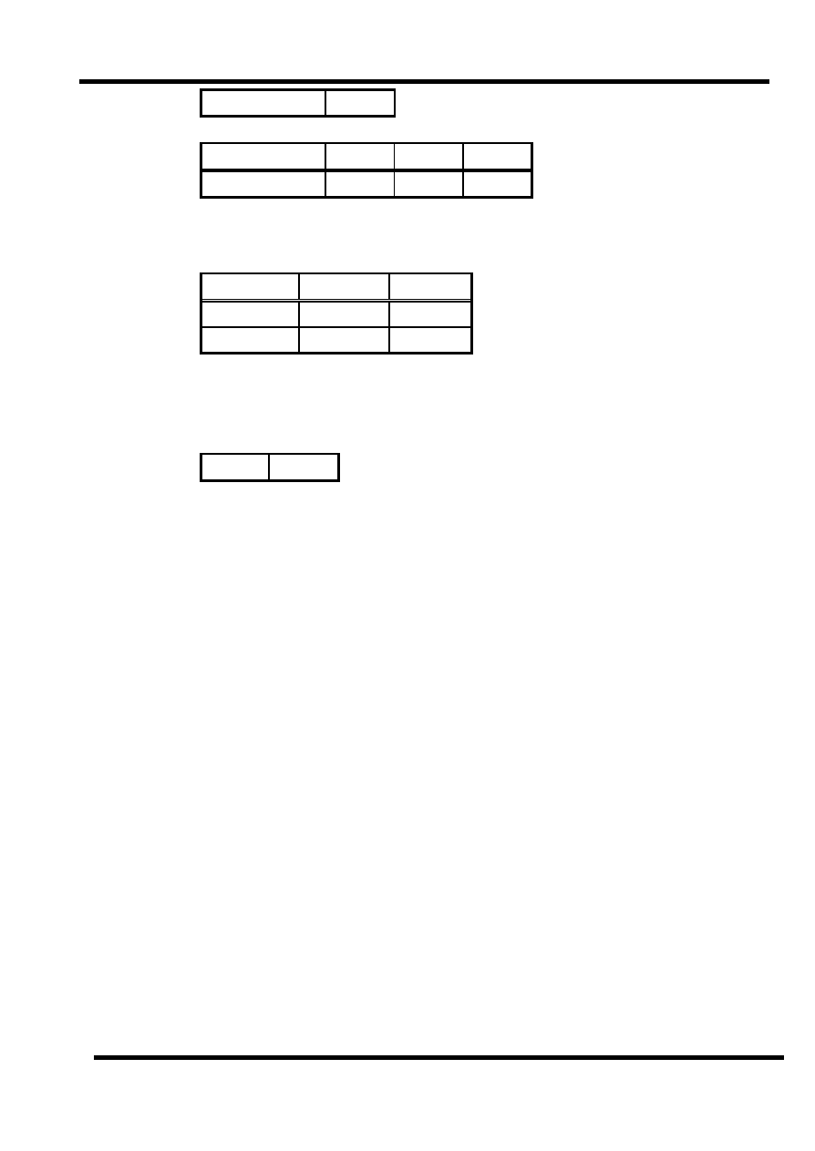
6. Memory Map
(A) Register Map
Address
Description
BANK0
00
Indirect Addressing Register
01
RTCC
02
PCL
03
STATUS
04
MSR
05
Port A
06
Port B
0A
PCH
0B
INTS
0C~2F
General purpose register
BANK1
01
TMR
05
CPIO A
06
CPIO B
07
PSTA

MD1060
This specification are subject to be changed without notice. Any latest information please preview
http;//www.mdtic.com.tw
P. 3
2002/10 Ver. 1.5
(1) IAR ( Indirect Address Register) : R00
(2) RTCC (Real Time Counter/Counter Register) : R01
(3) PC (Program Counter) : R02,R0A
Write PC --- from PCH
LJUMP, LCALL --- from instruction word
RTIW, RET,RTFI --- from STACK
A9
A8
A7~A0
Write PC --- from ALU
LJUMP, LCALL --- from instruction word
RTIW, RET, RTFI --- from STACK
(4) STATUS (Status register) : R03
Bit
Symbol
Function
0
1
2
3
4
5
7~6
C
HC
Z
PF
TF
RBS0
----
Carry bit
Half Carry bit
Zero bit
Power down Flag bit
WDT Timer overflow Flag bit
Register Bank Select bit :
0 : 00H --- 7FH
1 : 80H --- FFH
General purpose bit
(5) MSR (Memory Bank Select Register) : R4
Memory Bank Select Register :
0 : 00~7F
1 : 80~FF
b7
b6
b5
b4
b3
b2
b1
b0
Indirect Addressing Mode

MD1060
This specification are subject to be changed without notice. Any latest information please preview
http;//www.mdtic.com.tw
P. 4
2002/10 Ver. 1.5
(6) PORT A : R05
PA4~PA0, I/O Register
(7) PORT B : R06
PB7~PB0, I/O Register
(8)PCH (High byte of PC) : R0A
Bit
Function
1~0
High byte of PC
7~2
Unimplemented, reads as
`
0
'
(9) INTS ( Interrupt Status Register ) : R0B
Bit
Symbol
Function
0
RBIF
PORT B change interrupt flag. Set when PB <7:4> inputs change
1
INTF
Set when INT interrupt occurs. INT interrupt flag.
2
TIF
Set when TMR overflows.
3
RBIE
0 : disable PB change interrupt
1 : enable PB change interrupt
4
INTS
0 : disable INT interrupt
1 : enable INT interrupt
5
TIS
0 : disable TMR interrupt
1 : enable TMR interrupt
6
--
Unimplemented
7
GIS
0 : disable global interrupt
1 : enable global interrupt
(10) TMR (Time Mode Register) : R81
Bit
Symbol
Function
Prescaler Value
RTCC rate
WDT rate
2
--
0
PS2
--
0
0 0 0
0 0 1
0 1 0
0 1 1
1 0 0
1 0 1
1 1 0
1 1 1
1 : 2
1 : 4
1 : 8
1 : 16
1 : 32
1 : 64
1 : 128
1 : 256
1 : 1
1 : 2
1 : 4
1 : 8
1 : 16
1 : 32
1 : 64
1 : 128

MD1060
This specification are subject to be changed without notice. Any latest information please preview
http;//www.mdtic.com.tw
P. 5
2002/10 Ver. 1.5
Bit
Symbol
Function
3
PSC
Prescaler assignment bit :
0
--
RTCC
1
--
Watchdog Timer
4
TCE
RTCC signal Edge :
0
--
Increment on low-to-high transition on RTCC pin
1
--
Increment on high-to-low transition on RTCC pin
5
TCS
RTCC signal set :
0
--
Internal instruction cycle clock
1
--
Transition on RTCC pin
6
IES
Interrupt edge select
0
--
Interrupt on falling edge on PB0
1
--
Interrupt on rising edge on PB0
7
PBPH
PORTB pull-hi
0
--
PORTB pull-hi are enable
1
--
PORTB pull-hi are disable
(11) CPIO A (Control Port I/O Mode Register) : R85
"0", I/O pin in output mode;
"1", I/O pin in input mode.
(12) CPIO B (Control Port I/O Mode Register) : R86
"0", I/O pin in output mode;
"1", I/O pin in input mode.
(13) PSTA : R87
Bit Symbol
Function
0
PRDB
0:Power range-detector Reset occurred
1:No Power range-detector Reset Occurred
1
PORB
0:Power on Reset occurred
1:No Power on Reset occurred
(14) Configurable options for ROM :
Oscillator Type
RC Oscillator
HFXT Oscillator
XTAL Oscillator
LFXT Oscillator
Watchdog Timer control
Watchdog timer disable all the time
Watchdog timer enable all the time

MD1060
This specification are subject to be changed without notice. Any latest information please preview
http;//www.mdtic.com.tw
P. 6
2002/10 Ver. 1.5
Power-range control
Power-range disable
Power-range enable
Oscillator-start Timer control
0ms
80ms
Power-edge Detect
PED Disable
PED Enable
(B) Program Memory
Address
Description
000-3FF
Program memory
000
The starting address of power on, external reset or WDT time-out reset.
004
Interrupt vector
7. Reset Condition for all Registers
Register
Address
Power-On Reset,
Power range detector
Reset
/MCLR or WDT Reset
Wake-up from SLEEP
IAR
00h
RTCC
01h
xxxx xxxx
uuuu uuuu
uuuu uuuu
PC
0Ah,02h
00 0000 0000
00 0000 0000
00 0000 0100
STATUS
03h
0001 1xxx
000# #uuu
000# #uuu
MSR
04h
xxxx xxxx
uuuu uuuu
uuuu uuuu
PORT A
05h
- - -1 xxxx
- - -1 uuuu
- - -u uuuu
PORT B
06h
xxxx xxxx
uuuu uuuu
uuuu uuuu
INTS
0Bh
0000 0001
0000 000u
uuuu uuuu
TMR
81h
1111 1111
1111 1111
uuuu uuuu
CPIOA
85h
- - -1 1111
- - -1 1111
- - -u uuuu
CPIOB
86h
1111 1111
1111 1111
uuuu uuuu
PSTA
87h
- - - - - -qq
- - - - - -uu
- - - - --uu

MD1060
This specification are subject to be changed without notice. Any latest information please preview
http;//www.mdtic.com.tw
P. 7
2002/10 Ver. 1.5
Note : u
unchanged, x
unknown, -
unimplemented, read as "0"
#
value depends on the condition of the following table
Condition
Status: bit 4
Status: bit 3
Status: bit 1
Status: bit 0
/MCLR reset (not during SLEEP)
u
u
1
1
/MCLR reset during SLEEP
1
0
1
1
WDT reset (not during SLEEP)
0
1
1
1
WDT reset during SLEEP
0
0
1
1
Power on reset
1
1
0
X
Power range-detector Reset
1
1
1
0
8. Instruction Set :
Instruction Code
Mnemonic
Operands
Function
Operating
Status
010000 00000000
NOP
No operation
None
010000 00000001
CLRWT
Clear Watchdog timer
0
WT
TF, PF
010000 00000010
SLEEP
Sleep mode
0
WT, stop OSC
TF, PF
010000 00000011
TMODE
Load W to TMODE register
W
TMODE
None
010000 00000100
RET
Return from subroutine
Stack
PC
None
010000 00000rrr
CPIO R
Control I/O port register
W
CPIO r
None
010001 1rrrrrrr
STWR R
Store W to register
W
R
None
011000 trrrrrrr
LDR R, t
Load register
R
t
Z
111010 iiiiiiii
LDWI I
Load immediate to W
I
W
None
010111 trrrrrrr
SWAPR R, t
Swap halves register
[R(0~3)
R(4~7)]
t
None
011001 trrrrrrr
INCR R, t
Increment register
R + 1
t
Z
011010 trrrrrrr
INCRSZ R, t
Increment register, skip if zero
R + 1
t
None
011011 trrrrrrr
ADDWR R, t
Add W and register
W + R
t
C, HC, Z
011100 trrrrrrr
SUBWR R, t
Subtract W from register
R
W
t or
(R+/W+1
t)
C, HC, Z
011101 trrrrrrr
DECR R, t
Decrement register
R
1
t
Z
011110 trrrrrrr
DECRSZ R, t
Decrement register, skip if zero
R
1
t
None
010010 trrrrrrr
ANDWR R, t
AND W and register
R
W
t
Z
110100 iiiiiiii
ANDWI i
AND W and immediate
i
W
W
Z
010011 trrrrrrr
IORWR R, t
Inclu. OR W and register
R
W
t
Z
110101 iiiiiiii
IORWI i
Inclu. OR W and immediate
i
W
W
Z
010100 trrrrrrr
XORWR R, t
Exclu. OR W and register
R
W
t
Z

MD1060
This specification are subject to be changed without notice. Any latest information please preview
http;//www.mdtic.com.tw
P. 8
2002/10 Ver. 1.5
Instruction Code
Mnemonic
Operands
Function
Operating
Status
110110 iiiiiiii
XORWI i
Exclu. OR W and immediate
i
W
W
Z
011111 trrrrrrr
COMR R, t
Complement register
/R
t
Z
010110 trrrrrrr
RRR R, t
Rotate right register
R(n)
R(n-1),
C
R(7), R(0)
C
C
010101 trrrrrrr
RLR R, t
Rotate left register
R(n)
r(n+1),
C
R(0), R(7)
C
C
010000 1xxxxxxx
CLRW
Clear working register
0
W
Z
010001 0rrrrrrr
CLRR R
Clear register
0
R
Z
0000bb brrrrrrr
BCR R, b
Bit clear
0
R(b)
None
0010bb brrrrrrr
BSR R, b
Bit set
1
R(b)
None
0001bb brrrrrrr
BTSC R, b
Bit Test, skip if clear
Skip if R(b)=0
None
0011bb brrrrrrr
BTSS R, b
Bit Test, skip if set
Skip if R(b)=1
None
100nnn nnnnnnnn
LCALL n
Long CALL subroutine
n
PC,
PC+1
Stack
None
101nnn nnnnnnnn
LJUMP n
Long JUMP to address
n
PC
None
110111 iiiiiiii
ADDWI i
Add immediate to W
W+i
W
C,HC,Z
110001 iiiiiiii
RTIW i
Return, place immediate to W
Stack
PC,i
W
None
111000 iiiiiiii
SUBWI i
Subtract W from immediate
i-W
W
C,HC,Z
010000 00001001
RTFI
Reture from interrupt
Stack
PC,1
GIS
None
Note :
W
:
Working register
b
:
Bit position
WT
:
Watchdog timer
t
:
Target
TMODE
:
TMODE mode register
0
:
Working register
CPIO
:
Control I/O port register
1
:
General register
TF
:
Timer overflow flag
R
:
General register address
PF
:
Power loss flag
C
:
Carry flag
PC
:
Program Counter
HC :
Half carry
OSC
:
Oscillator
Z
:
Zero flag
Inclu.
:
Inclusive `
'
/
:
Complement
Exclu.
:
Exclusive `
'
x
:
Don't care
AND
:
Logic AND `
'
i
:
Immediate data ( 8 bits )
n
:
Immediate address

MD1060
This specification are subject to be changed without notice. Any latest information please preview
http;//www.mdtic.com.tw
P. 9
2002/10 Ver. 1.5
9. Electrical Characteristics
*Note: Temperature=25�C
1. Operation Current :
(1) HF (C=10p) , WDT - enable, PRD � disable
4M
10M
20M
Sleep
2.5V
300u
670u
1.4m
1u
3.0V
410u
880u
1.8m
2.5u
4.0V
650u
1.4m
2.6m
6.4u
5.0V
1m
1.9m
3.4m
12u
6.4V
1.5m
2.8m
4.9m
26u
(2) XT (C=10p) , WDT - enable, PRD � disable
1M
4M
10M
Sleep
2.5V
100u
300u
700u
1u
3.0V
135u
380u
850u
2.5u
4.0V
240u
600u
1.35m
6.4u
5.0V
400u
900u
1.8m
12u
6.4V
720u
1.4m
2.6m
26u
(3) RC, WDT - Enable; PRD - Disable; @Vdd = 5.0V
C
R
Freq.
Current
4.7k
10.2M
1.8m
10k
5.64M
1.1m
47k
1.35M
300u
100k
654K
180u
300k
223K
100u
3p
470k
144K
80u
4.7k
4.78M
900u
10k
2.47M
500u
47k
560K
150u
100k
268K
100u
300k
90K
70u
20p
470k
58K
60u

MD1060
This specification are subject to be changed without notice. Any latest information please preview
http;//www.mdtic.com.tw
P. 10
2002/10 Ver. 1.5
C
R
Freq.
Current
4.7k
1.43M
320u
10k
721K
200u
47k
158K
90u
100k
75.4K
70u
300k
25.2K
60u
100p
470k
16.2K
55u
4.7k
641K
180u
10k
320K
120u
47k
70K
70u
100k
33.3K
60u
300k
11.1K
50u
300p
470k
7.1K
48u
(4) LF (C=10p) , WDT - enable, PRD - disable,
32K
455K
1M
Sleep
2.5V
5u
40u
80u
1u
3.0V
8u
55u
100u
2.5u
4.0V
19u
85u
150u
6.4u
5.0V
45u
130u
200u
12u
6.4V
190u
195u
300u
26u
2. Input Voltage (Vdd = 5V) :
Port
Min
Max
TTL
Vss
1.0V
Vil
Schmitt trigger
Vss
1.0V
TTL
2.2V
Vdd
Vih
Schmitt trigger
3.5V
Vdd
3. Output Voltage (Vdd = 5V) :
PA,PB
Condition
Voh
3.7V
Ioh = -20mA
Vol
0.5V
Iol = 20mA
Voh
4.6V
Ioh = -5mA
Vol
0.3V
Iol = 5mA

MD1060
This specification are subject to be changed without notice. Any latest information please preview
http;//www.mdtic.com.tw
P. 11
2002/10 Ver. 1.5
4. Output Current (Max.) (Vdd = 5V) :
Port A:
Current
source current
30mA
sink current
50mA
Port B:
Current
source current
30mA
sink current
50mA
5. The basic WDT time-out cycle time :
time
2.5V
25
3.0V
22
4.0V
19
5.0V
17
6.3V
15
Unit = ms
6. PRD :
(1)PRD reset voltage :
Voltage
Vh
4.2
�
5%
Vl
3.8
�
5%
Unit = V
(2) PRD reset current :
Current
4.2V
100
3.8V
80
Unit = uA
7. Min Operation Voltage :
C =>
10p
20p
30p
XT, 20M
2.5
2.5
2.5
HF, 20M
2.5
2.5
2.5
Unit = V
MD1060
This specification are subject to be changed without notice. Any latest information please preview
http;//www.mdtic.com.tw
P. 12
2002/10 Ver. 1.5
RC, 1k, no cap.
2.5
Unit = V
C =>
0p
10p
20p
LF, 1M
2.6
2.9
3.1
Unit = V
8. Pull high/low resistor :
Vdd
5V
3V
Pull high
35
65
Pull low
35
65
Unit = kOhm
9. MCLR filter time :
Vdd=5V
time
600
Unit = ns