
MDT10P65
This specification are subject to be changed without notice. Any latest information
please preview http;//www.mdtic.com.tw
P.1 2005/10 Ver1.6
1. General Description
This OTP-Based 8-bit micro-controller
uses a fully static CMOS technology
process to achieve higher speed and
smaller size with the low power
consumption and high noise immunity. On
chip memory includes 4K words of
EPROM, and 192 bytes of static RAM.
2. Features
RISC CPU
Fully static design
37 single word instructions
4K x 14 program memory.
192 bytes RAM for data
35 bi-directional I/O
Eight level hardware stacks
Watchdog timer with on-chip RC
oscillator.
Interrupt capability
Timer0 : 8-bit timer with 8-bit
prescaler
Timer1 : 8-bit timer with 8-bit compare
register. This timer can be used as
carrier generator.
Sleep mode for power saving.
PB and PD with port change wake-up
interrupt.
3. Applications
The application areas of this MDT10P65
range from appliance motor control and high
speed automotive to low power remote
transmitters/receivers and
telecommunications processors, such as
Remote controller, small instruments, toy,
automobile and keyboard ... etc.
PS : timer1 counter PC0 clock in low to high
the counter data increase

MDT10P65
This specification are subject to be changed without notice. Any latest information
please preview http;//www.mdtic.com.tw
P.2 2005/10 Ver1.6
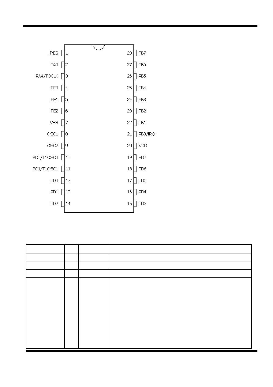
4. Pin Diagram
MDT10P65A3P/S 18 pin DIP/SOP
MDT10P65SD42 pin Shrink PDIP
PA6 1
42 PA7
/RES 2
41 PB7
PA0 3
40 PB6
PA1 4
39 PB5
PA2 5
38 PB4
PA3 6
37 PB3
PA4/T0CLK 7
36 PB2
PA5 8
35 PB1
PE0 9
34 PB0/IRQ
PE1 10
33 VDD
PE2 11
32 VSS
VDD 12
31 PD7
/RES 1
18 PB4
VSS 13
30 PD6
PA2 2
17 PB3
OSC1 14
29 PD5
PA3 3
16 PB2
OSC2 15
28 PD4
PA4 4
15 PB1
PC0/T1OSCO 16
27 PC7
VSS 5
14 PB0
PC1/T1OSCI 17
26 PC6
OSC1 6
13 VDD
PC2 18
25 PC5
OSC2 7
12 PC7
PC3 19
24 PC4
PC0/T1OSCO 8
11 PC6
PD0 20
23 PD3
PC1/T1OSCI 9
10 PC5
PD1 21
22 PD2
MDT10P65A1Q
MDT10P65A2Q
MDT10P65
This specification are subject to be changed without notice. Any latest information
please preview http;//www.mdtic.com.tw
P. 3
2005/10
Ver. 1.6
MDT10P65 pin 28 PDIP/SOP
5. Pin function description
Pin name
Type Buffer type
Description
OSC1 I Oscillator
input
OSC2 O Oscillator
out
/RES(MCLRB) I
ST
Reset input with 130K ohm pull-up
PA0
PA1
PA2
PA3
PA4
PA5
PA6
PA7
I/O
I/O
I/O
I/O
I/O
I/O
I/O
I/O
TTL
TTL
TTL
TTL
ST
TTL
TTL
TTL
Bi-directional I/O port A. Port A can be software
programmed for internal 45K ohm pull-up on all pins
except PA5. The pull-up resistance on PA5 is 100K ohm.
Can be clock input to Timer0.

MDT10P65
This specification are subject to be changed without notice. Any latest information
please preview http;//www.mdtic.com.tw
P. 4
2005/10
Ver. 1.6
Pin name Type Buffer type
Description
PB0/IQR
PB1
PB2
PB3
PB4
PB5
PB6
PB7
I/O
I/O
I/O
I/O
I/O
I/O
I/O
I/O
ST/TTL
TTL
TTL
TTL
TTL
TTL
TTL
TTL
Bi-directional I/O port B. Port B can be software
programmed for internal 25K ohm pull-up on all pins.
PB0-PB7 can generate interrupt on pin state change.
Can be the external interrupt pin.
PC0
PC1
PC2
PC3
PC4
PC5
PC6
PC7
I/O
I/O
I/O
I/O
I/O
I/O
I/O
I/O
ST
ST
ST
ST
ST
ST
ST
ST
Bi-directional I/O port C. Port C can be software
programmed for internal 100K pull-up on all pins.
Can be Timer1 oscillator output or Timer1 clock input.
Can be Timer1 oscillator input.
PD0-PD7 I/O
ST
Bi-directional port. All pins can generate interrupt on pin
state change. Port D can be software programmed for
internal 100K pull-up on all pins.
PE0
PE1
PE2
I/O
I/O
I/O
ST
ST
ST
Bi-directional port E. Port E can be software programmed
for internal 100K pull-up on all pins.
Vdd
Power
input
Vss
Ground
pin

MDT10P65
This specification are subject to be changed without notice. Any latest information
please preview http;//www.mdtic.com.tw
P. 5
2005/10
Ver. 1.6
6. Memory
Mapping
6.1Program memory :
0000h Reset
Vector
0001h
0002h
0003h
0004h Peripheral
interrupt
Vector
0005h
Program
memory
(Page
0)
07FFh
0800h
Program
memory
(Page
1)
0FFFh
6.2Register file map :
BANK 0
BANK 1
00h IAR
IAR 80h
01h RTCC
TMR 81h
02h PCL
PCL 82h
03h STATUS STATUS 83h
04h MSR
MSR 84h
05h PORT A
CPIO A
85h
06h PORT B
CPIO B
86h
07h PORT C
CPIO C
87h
08h PORT D
CPIO D
88h
09h PORT E
CPIO E
89h
0Ah PCH
PCH 8Ah
0Bh INTS
INTS 8Bh
0Ch PIFB1
PIEB1 8Ch
0Dh
PIFB2
PIEB2
8Dh
0Eh TMR1L
PSTA 8Eh
0Fh
8Fh
10h T1STA
PPHE
90h
11h
91h
12h
92h
13h
93h
14h
94h
15h
CCP1L
95h
16h
96h
17h CCP1CTL
97h
18h
98h
1Fh
9Fh
20h
A0h
General
General
Purpose Purpose
Register Register
7Fh
FFh
Unimplemented memory location.