
MDT75C272
OTP Encoder
This specification is subject to be changed without notice. Please visit our web site for the most updated information.
http://www.mdtic.com.tw
1 of 5
2005/6/20 Ver. 1.3
1. General Description
The MDT75C272 is an OTP Encoder using CMOS technology. It has a maximum of 20 bits addressing code
providing up to one million codes. It can reduce any code collision and unauthorized code scanning possibilities.
2. Features
l
CMOS technology.
l
Low standby current : 1.0 uA.
l
Wide range of Operating Voltage : Vdd = 3.0V ~ 12V.
l
Up to 4 data pins.
l
Total 1048576 address codes.
l
Built-in RC oscillator with single external resistor.
l
Available in DIP and SOP package.
l
Automatically enter sleep mode if press button over 6 ~ 10 sec
3. Pin Assignment
MDT75C272P / 75C272S
8 pin DIP / SOP
OSCR 1
8 K3
Vdd 2
7 K2
Vss 3
6 K1
TXD 4
5 K0
4. Pin Function Description
Symbol
I/O
Function Description
OSCR
I
Connect a resistor to Vdd to adjust internal RC freq.
Vdd
Positive power supply 3.0V ~ 12 V.
Vss
Ground.
TXD
O
Data output pin.
K0
I
Data input with pull low Resistor.
K1
I
Data input with pull low Resistor.
K2
I
Data input with pull low Resistor.
K3
I
Data input with pull low Resistor.
MDT75C272
OTP Encoder
This specification is subject to be changed without notice. Please visit our web site for the most updated information.
http://www.mdtic.com.tw
2 of 5
2005/6/20 Ver. 1.3
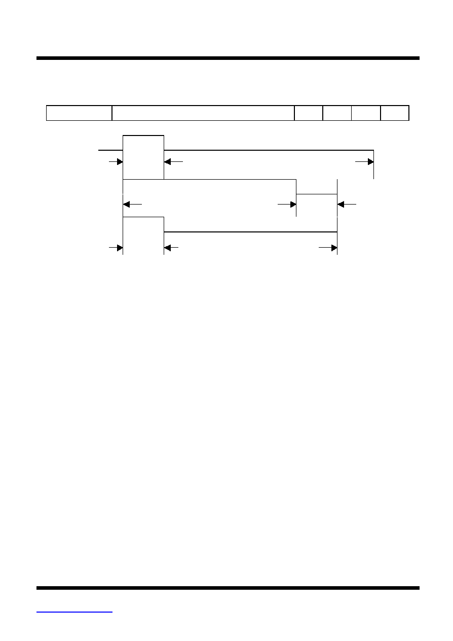
5.Output Data Reporting
Output data frame
Preamble
C0 ~ C19 ( 1048576 address codes )
D0
D1
D2
D3
Preamble :
4 Ick 636 Ick for 75C272
Data High :
12 Ick
4 Ick
Data Low :
4 Ick
12 Ick
Note : 1 Ick = 8 OSC clocks
6. Key 0 ~ 3 combination table
K3
K2
K1
K0
D3
D2
D1
D0
0
0
0
1
0
0
0
1
0
0
1
0
0
0
1
0
0
0
1
1
0
0
1
1
0
1
0
0
0
1
0
0
0
1
0
1
0
1
0
1
0
1
1
0
0
1
1
0
0
1
1
1
0
1
1
1
1
0
0
0
1
0
0
0
1
0
0
1
1
0
0
1
1
0
1
0
1
0
1
0
1
0
1
1
1
0
1
1
1
1
0
0
1
1
0
0
1
1
0
1
1
1
0
1
1
1
1
0
1
1
1
0
1
1
1
1
1
1
1
1

MDT75C272
OTP Encoder
This specification is subject to be changed without notice. Please visit our web site for the most updated information.
http://www.mdtic.com.tw
3 of 5
2005/6/20 Ver. 1.3
7. Absolute Maximum Rating
Symbol
Parameter
Conditions
Rating
Unit
Vdd
Supply Voltage
-0.3 ~ 13
V
Vi
Input Voltage
-0.3 ~ Vdd+0.3
V
Vo
Output Voltage
-0.3 ~ Vdd+0.3
V
Tst
Storage Temp.
-40 ~ 125
Top
Operating Temp.
-20 ~ 70
Pdis
Max. Power dissipation
Vdd = 12V
300
mV
8. DC Electrical Characteristics (T
A
=0
to 70
)
Symbol
Parameters
Conditions
Min.
Typ.
Max.
Unit
Vdd
Operating Voltage
3.0
5
12
V
Isb
Stand by current
Vdd = 12V, OSC stop
K0 ~ K3 = Low
Output Unloaded
1.0
3.0
uA
Iop
Operating current
Vdd =12V
0.5
1.0
mA
Ioh
Source current
Vdd =12V, Voh = 6V
4.5
mA
Iol
Sink Current
Vdd =12V, Vol = 6V
4.5
mA
Fop
Operating Freq
Vdd=11V,
Rosc=360K ~ 470K ohm
80K
HZ

MDT75C272
OTP Encoder
This specification is subject to be changed without notice. Please visit our web site for the most updated information.
http://www.mdtic.com.tw
4 of 5
2005/6/20 Ver. 1.3
1
2
3
4
5
6
7
8
VDD
VSS
TXD
K3
K2
K1
K0
OSCR
R
OSC
Vdd
Vss
Transmitter
Circuit
SW0
SW1
SW2
SW3
9.
Application circuit
10.External oscillator resistor selection table (Vdd=11V)
Rosc (ohm)
Freq. (Hz)
Operating Current
510 K
70.0 K
443
µ
A
470 K
74.0 K
444
µ
A
430 K
78.7 K
445
µ
A
390 K
84.6 K
447
µ
A
360 K
88.9 K
449
µ
A
330 K
97.4 K
451
µ
A
