
MLX90224
Dual Hall Effect Switch
3901090224
Page 1 of 10
Data Sheet
Rev. 005
July/03
Features and Benefits
Chopper Stabilized Amplifier Stage
CMOS for Optimum Stability, Quality and Cost
Dual Output
5V to 24V Operation
Phase/Direction Detection (option code B)
Applications
Direction Detector
Speed Sensor
Shaft Encoding
Position Sensing
Ordering Information
Part No.
Temperature Suffix
Package Code
Option code
MLX90224
E (-40∞C to 85∞C)
VA
A
MLX90224
E (-40∞C to 85∞C)
VA
B
1. Functional Diagram
Voltage
Regulator
Chopper
Chopper
1
2
3
4
Replaced with Logic for
MLX90224 B
MLX90224EVA-A MLX90224EVA-B
Pin 1
V
DD
V
DD
Pin 2
Switch Plate 1
Speed
Pin 3
GND
GND
Pin 4
Switch Plate 2
Direction
2. Description
The MLX90224 series are dual Hall effect
switches. It includes two Hall effect switch
functions of which typical thresholds are +/- 2.0
mT. In each switch, the magnetic flux detection
is performed by a switched silicon Hall plate.
The B
OP
and B
RP
are temperature-compensated
and give a sensitivity temperature coefficient of
500 ppm/
o
C to compensate popular magnets.
The MLX90224LVAA output transistor will be
"switched on" (B
OP
) in the presence of a
sufficiently strong South pole magnetic field
facing the marked side of the package. Similarly,
the output will be "switched off" (B
RP
) in the
presence of a North field. Spacing on the plates
is 1.85mm.
The MLX90224LVAB serie is designed for
direction detection with a high speed chopper.
The output structure is an Open-Drain NMOS
transistor with a capability of 25 mA.

MLX90224
Dual Hall Effect Switch
3901090224
Page 2-2 of 10
Data Sheet
Rev. 005
July/03
TABLE OF CONTENTS
FEATURES AND BENEFITS ....................................................................................................................... 1
APPLICATIONS............................................................................................................................................ 1
ORDERING INFORMATION......................................................................................................................... 1
1.
FUNCTIONAL DIAGRAM................................................................................................................... 1-1
2.
DESCRIPTION.................................................................................................................................... 2-1
3.
GLOSSARY OF TERMS ....................................................................................................................... 3
4.
ABSOLUTE MAXIMUM RATINGS ....................................................................................................... 3
5.
MLX90224 ELECTRICAL SPECIFICATIONS ...................................................................................... 3
6.
MLX90224 SENSOR SPECIFIC SPECIFICATIONS ............................................................................ 4
7.
GENERAL DESCRIPTION .................................................................................................................... 4
8.
PERFORMANCE GRAPHS................................................................................................................... 5
9.
APPLICATIONS INFORMATION.......................................................................................................... 6
10.
RELIABILITY INFORMATION............................................................................................................... 8
11.
ESD PRECAUTIONS............................................................................................................................. 8
12.
PACKAGE INFORMATION................................................................................................................... 9
13.
DISCLAIMER....................................................................................................................................... 10

MLX90224
Dual Hall Effect Switch
3901090224
Page 3 of 10
Data Sheet
Rev. 005
July/03
3. Glossary of Terms
Gauss, Tesla: Two units to quantify a magnetic flux density. Conversion: 1 mT = 10 Gauss
Bop: B Operating Point: When the magnetic flux density increases and reaches the Bop value, the output
switches on. This value is in Gauss.
Brp: B Release Point: When the magnetic flux density decreases and reaches the Brp value, the output
switches off. This value is in Gauss.
4. Absolute Maximum Ratings
Supply Voltage, V
DD
24
V
Supply Current, I
DD
50
mA
Output Current, I
OUT
40
mA
Output Short-Circuit Current
150 mA
Operating Temperature Range, T
A
-40∞C to 150∞C
Storage Temperature Range, T
S
-65∞C to 150∞C
Maximum Junction Temp, T
J
+
175∞C
Magnetic Flux Density
Infinite
Exceeding the absolute maximum ratings may cause permanent damage. Exposure to absolute-
maximum-rated conditions for extended periods may affect device reliability.
5. MLX90224 Electrical Specifications
DC Operating Parameters T
A
= -40
o
C to 85
o
C, V
DD
= 5V to 24V (unless otherwise specified)
Parameter Symbol
Test
Conditions
Min
Typ
Max
Units
Supply Voltage
V
DD
Operating
5
24
V
Supply Current
I
DD
3.0 7.5 10
mA
Output Current
I
OUT
B>B
OP
20
mA
Saturation Output Voltage
V
SAT
B>B
OP,
I
OUT
=20 mA
200
600
mV
Output Voltage
V
OUT
B<B
RP
24
V
Output Leakage
I
LEAK
10
µA
Refresh Time
Tr
7
15
µS

MLX90224
Dual Hall Effect Switch
3901090224
Page 4 of 10
Data Sheet
Rev. 005
July/03
6. MLX90224 Sensor Specific Specifications
DC Operating Parameters T
A
= -40
o
C to 85
o
C, V
DD
= 5V to 24V (unless otherwise specified)
Parameter Symbol
Test
Conditions
Min
Typ
Max
Units
Operate Point
B
OP
-
2.5 5.5
mT
Release Point
B
RP
-5.5 -2.5 -
mT
Hysteresis B
HYS
1.0 4.0 7.5 mT
Note:
1 mT = 10 Gauss
7. General Description
The MLX 90224 is designed for use with multipole ring magnet targets having evenly distributed North
and South magnetic poles on the circumference of the target. An example of the basic physical
arrangement of the sensor and magnet is shown in Fig. 1. The MLX90224 is available in 2 versions. The
first version provides the user with two digital output signals. Output S1 will provide a speed pulse from
the changing magnetic flux at sensing element S1. Output S2 will provide a phase shifted (d = 1.85 mm)
output identical in pulse width and period to S1. This version is referred to as MLX90224LVAA. The
MLX90224LVAB version provides an output signal that decodes the phase shifted signals to directly
provide an output for the speed which is twice the rotation speed of the target. The other output pin
represent the direction and changes from logic-high to logic-low when the direction of rotation of the
magnet is reversed. It allows to directly see the condition of the speed with twice the resolution of the
MLX90224LVAA and to also know directly the direction of rotation of the target. The MLX90224LVAA has
switching magnetic Bop and Brp values of typically +/- 2.5 mT as does the internal circuitry of the LVAB.
N
S
N
S
N
N
S
N
S
N
S
N
N
S
N
S
N
S
N
S
N
S
N
S
N
S
N
S
N
S
N
S
N
S
N
S
N
S
S
S
Figure 1: Application with a multipole ring magnet

MLX90224
Dual Hall Effect Switch
3901090224
Page 5 of 10
Data Sheet
Rev. 005
July/03
8. Performance Graphs
5
-5
Fl
ux
Dens
i
t
y
(m
T)
Temperature (
o
C)
Typical Magnetic Switch Points
versus
Temperature
90224 A, B
80
-3
-1
1
3
0
-40
120
160
200
40
B
OP
B
RP
0
25
O
u
t
put
V
o
lt
age (V
)
Flux Density (mT)
Output Voltage
versus
Flux Density
90224 A, B
0
5
10
15
20
-2
-4
-6
2
4
6
0
V
DD
V
sat
B
OP
B
RP
10
0
S
uppl
y
Current
(m
A
)
Supply Voltage (V)
Typical Supply Current
versus
Supply Voltage
90224
15
2
4
6
8
10
5
0
20
25
30
T
A
= -40
o
C
T
A
= 25
o
C
T
A
= 85
o
C
500
0
V
DS(
O
N)
(mV
)
Temperature (
o
C)
Typical Saturation Voltage
versus
Temperature
V
DD
= 12 V, I
OUT
= 20mA
90224
80
100
200
300
400
0
-40
120
160
200
40
V
DS(ON)

MLX90224
Dual Hall Effect Switch
3901090224
Page 6 of 10
Data Sheet
Rev. 005
July/03
9. Applications Information
Severe Environment and
Automotive Protection Circuit
V
DD
In severe cases it may be necessary to include a Zener diode to clamp positive
interference and Schottky diodes to clamp negative excursions.
C2
R3
R1, R2 = 5.6k
R3 = 332
C1 = 10nF
C2 = 2.2nF
V
DD
C1
R1
Output
MLX
90224
C2
R2
Output

MLX90224
Dual Hall Effect Switch
3901090224
Page 7 of 10
Data Sheet
Rev. 005
July/03
0
20
40
60
80
100
120
140
160
180
200
-40
-20
0
20
40
60
time (ms)
Magnetic
Field (G)
Bop
Brp
Out 1
Out 2
B1
B2
Timing diagram when applied a B1-B2 quadratic
magnetic field on MLX90224, LVAA version
0
50
100
150
200
250
300
350
400
-50
0
50
time
Bop
Brp
Magnetic
Field (G)
B1
B2
Signal from
Plate 1
Signal from
Plate 2
Speed output
Direction
output
Timing diagram when applied a B1-B2 quadratic magnetic
field on MLX90224, LVAB version (direction and speed
outputs)

MLX90224
Dual Hall Effect Switch
3901090224
Page 8 of 10
Data Sheet
Rev. 005
July/03
10. Reliability
Information
Melexis devices are classified and qualified regarding suitability for infrared, vapor phase and wave
soldering with usual (63/37 SnPb-) solder (melting point at 183degC).
The following test methods are applied:
IPC/JEDEC J-STD-020A (issue April 1999)
Moisture/Reflow Sensitivity Classification For Nonhermetic Solid State Surface Mount Devices
CECC00802 (issue 1994)
Standard Method For The Specification of Surface Mounting Components (SMDs) of Assessed Quality
MIL 883 Method 2003 / JEDEC-STD-22 Test Method B102
Solderability
For all soldering technologies deviating from above mentioned standard conditions (regarding peak
temperature, temperature gradient, temperature profile etc) additional classification and qualification tests
have to be agreed upon with Melexis.
The application of Wave Soldering for SMD's is allowed only after consulting Melexis regarding assurance
of adhesive strength between device and board.
For more information on manufacturability/solderability see quality page at our website:
http://www.melexis.com/
11. ESD
Precautions
Electronic semiconductor products are sensitive to Electro Static Discharge (ESD).
Always observe Electro Static Discharge control procedures whenever handling semiconductor products.
MLX90224
Dual Hall Effect Switch
3901090224
Page 9 of 10
Data Sheet
Rev. 005
July/03
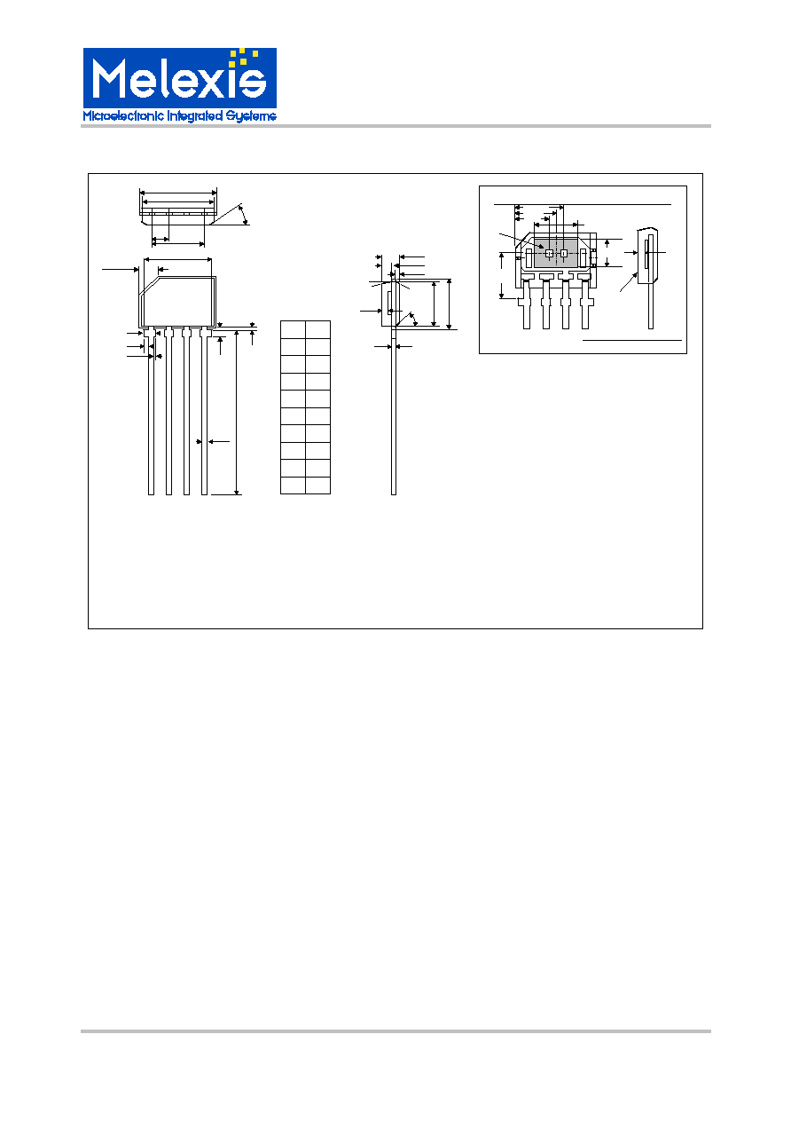
12. Package Information
VA Package
Dimensions
Notes:
1. Pinout:
Pin 1
Vdd
Pin 2
Latch Plate 1/ Speed
Pin 3
GND
Pin 4
Latch Plate 2 / Direction
2. Controlling dimension: mm .
3. Leads must be free of flash and plating voids.
4. Leads must not arc toward the rear of package.
5. Package dimensions exclude molding flash.
6. Tolerance: +/- 0.254 mm unless otherwise specified.
7. Marking:
Line 1:
3 first digits (224)
4th and 5th digits (XA)
= Version A (double latch)
Line 2:
5 digits (ZZZZZ)
=Part Number MLX90224
Back Side Marking
=Lot Number
E
3. 46
3. 30
A
B
C
5o
(2x)
5o
(2x)
0.387
0.289
3 .79
3 .63
D
F
G
H
1.0
MAX
0.22
REF
0.45
0.35
4.50
4.10
45 o X 1mm
15.50
14.50
224XA
ZZZZZ
1
2
3
4
5.08
5.24
5.33
5.43
1.22
1.32
3.76
3.86
J
VA
1.20
1.10
0.66
0.61
0.29
0.24
45 o
0.31
0.18
B
A
C
D
E
0.15
0.0
F
G
H
0.60
0.40
0.35
0.25
J
45 o
4 digits (WWYY) =Date Code
All Dimensions in millimeters
VA Hall Plate / Chip Location
2.180
Hall Plates
0.25 x 0.25
2.69
0.387
0.289
Marked
Surface
1.700
2.700
1.765
3.615
(XB)
= Version B (Speed-Direction)

MLX90224
Dual Hall Effect Switch
3901090224
Page 10 of 10
Data Sheet
Rev. 005
July/03
13. Disclaimer
Devices sold by Melexis are covered by the warranty and patent indemnification provisions appearing in
its Term of Sale. Melexis makes no warranty, express, statutory, implied, or by description regarding the
information set forth herein or regarding the freedom of the described devices from patent infringement.
Melexis reserves the right to change specifications and prices at any time and without notice. Therefore,
prior to designing this product into a system, it is necessary to check with Melexis for current information.
This product is intended for use in normal commercial applications. Applications requiring extended
temperature range, unusual environmental requirements, or high reliability applications, such as military,
medical life-support or life-sustaining equipment are specifically not recommended without additional
processing by Melexis for each application.
The information furnished by Melexis is believed to be correct and accurate. However, Melexis shall not
be liable to recipient or any third party for any damages, including but not limited to personal injury,
property damage, loss of profits, loss of use, interrupt of business or indirect, special incidental or
consequential damages, of any kind, in connection with or arising out of the furnishing, performance or
use of the technical data herein. No obligation or liability to recipient or any third party shall arise or flow
out of Melexis' rendering of technical or other services.
© 2002 Melexis NV. All rights reserved.
For the latest version of this document, go to our website at:
www.melexis.com
Or for additional information contact Melexis Direct:
Europe and Japan:
All other locations:
Phone: +32 13 67 04 95
Phone: +1 603 223 2362
E-mail: sales_europe@melexis.com E-mail:
sales_usa@melexis.com
QS9000, VDA6.1 and ISO14001 Certified