 | –≠–ª–µ–∫—Ç—Ä–æ–Ω–Ω—ã–π –∫–æ–º–ø–æ–Ω–µ–Ω—Ç: MLX90719 | –°–∫–∞—á–∞—Ç—å:  PDF PDF  ZIP ZIP |

MLX902xx Name of Sensor
Rev Y.X
22/Aug/98
Page 1
MLX90719
General purpose timer
3901090719
Page 1
Aug/02
Rev. 002
Features and Benefits
1
µ
m CMOS technology
MLX8 core with 8 accumulators, 80 bytes RAM and 6K ROM
1 high voltage input (detection of mains-active)
Zero-crossing detection input to detect the 50/60Hz
7 standard inputs of which 2 can be used as comparator inputs and 2 can be configured
as open-collector outputs.
15 configurable LCD outputs (segment/backplane)
3 relay drivers which can also be used to drive a triac or LED's without the need for ex-
ternal resistors.
Buzzer driver with programmable frequency
On-chip 4MHz oscillator, crystal oscillator and low power RC oscillator
Low power mode (battery or decoupling capacitor)
High supply voltage eliminates the need for high power resistors
Battery backup
On-chip watchdog
Applications
24 hour timer for cooker applications, coffee maker, ...
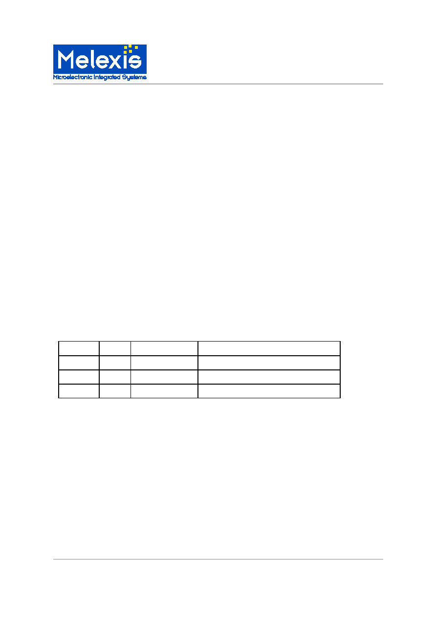
Ordering Information
Part No.
Temperature Suffix
Package Code
Option Code
MLX90719
C ( 0∞C to 70∞C )
DF (SOIC 16, 300mil) -x
The customer specific version code (defining the ROM content) is indicated with 1 character at the end of the
ordering number.
Description
The ASIC consists of a dedicated microcontroller
combined with on-chip analog and digital blocks,
which can be configured to a great extend. This
makes it ideal to adapt it to different applications by
means of an update in the software. The number of
external components for the electronic module is
minimized. A typical application mainly consists of
the MLX90719 ASIC, a number of command buttons,
a LCD, a relay, some LED's and a buzzer.
The number of buttons and their function can be
freely chosen. The configuration of the LCD, the
number of backplanes and its pinout is also under
software control. Three outputs are available for a
relay and LED's.
Functional Diagram
MLX90719
LX11
Interrupt
controller
RAM
1 x comp
Counter
W atchdog
XT1
XT2
IN 1-8
ZCD
VDD4
BAT
VSS
LCD 1-15
OUT A,B,C
BUZ
17bit timer
Controller
125kHz
oscillator
4MHz
PLL
LC
oscillator
POR
8 x input
Vreg
Xtal
LCD
Output
A, B, C
Buzzer
Zero
cross

MLX90719
General purpose timer
3901090719
Page 2
Aug/02
Rev. 002
General description
The MLX90719 is an ASIC which is ideally suited
for timing control application, low cost as well as
high end, such as clocks in coffee machines, cook-
ers, baking equipment,...
The ASIC consists of a dedicated microcontroller
combined with on-chip analog and digital blocks,
which can be configured to a great extend. This
makes it ideal to adapt it to different applications by
means of an update in the software. The number of
external components for the electronic module is
minimized. A typical application mainly consists of
the MLX90719 ASIC, a number of command but-
tons, a LCD, a relay, some LED's and a buzzer.
The number of buttons and their function can be
freely chosen. The configuration of the LCD, the
number of backplanes and its pinout is also under
software control. Three outputs are available for a
relay and LED's.
Main functions:
General-purpose timer chip based on the 8-bit
LX11 core, including 80 bytes RAM and 6 Kbytes
ROM.
Programming of the ROM and selection of all other
options is done with one mask.
An interrupt controller guarantees exact timings
and a clean refresh rate of the LCD.
High supply voltage eliminates the need for high
power resistors.
6 digital inputs and 2 I/O pins (function is under
software control).
1 comparator (uses 2 of the digital inputs) which
can be used for analog measurements.
3 high current output drivers. They are suitable for
driving low cost 12V relays, but other types can
also be used. They can also be used to drive triac
or LED's without the need for external resistors.
1 buzzer output for piezo electric buzzers, with
programmable frequency.
The LCD interface consists of 15 outputs, each of
them can be configured as backplane or segment
driver.
The time base for the clock function is derived ei-
ther from the mains frequency or from a crystal
oscillator.
The clock frequency for the microcontroller, relay
drivers and buzzer output is derived from an on
chip oscillator, which is calibrated under software
control.
For applications that are disconnected from the
mains for longer times, a battery backup can be
foreseen, so that the module always keeps track of
the time.
For short mains interruptions (up to 5 minutes), the
energy in a decoupling capacitor can be used to
keep track of the time.
An on-chip watchdog ensures the functioning of the
chip under all environmental conditions.
The package size can be adapted to the number of
used pins (non-used I/O's do not need to be
bonded).
MLX902xx Name of Sensor
Rev Y.X
22/Aug/98
Page 3
MLX90719
General purpose timer
3901090719
Page 3
Aug/02
Rev. 002
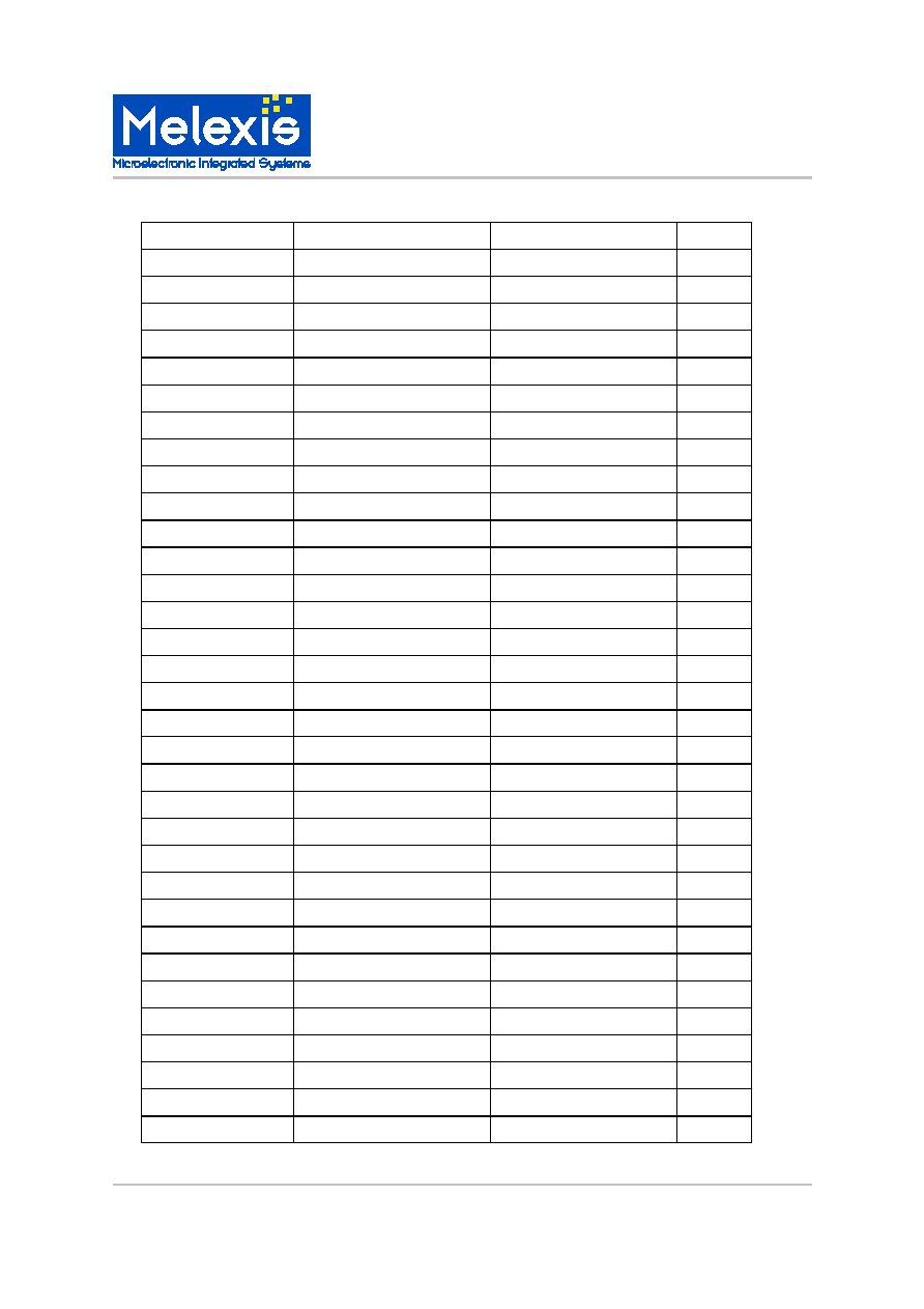
MLX90719 Electrical Specifications
Parameter
Symbol Test Conditions
Min Typ Max Units
Ambient temperature
Tamb
0
85
∞C
Maximum chip temperature Tic
150 ∞C
Maximum allowed source
supply current
Idd4m
Drivers off = all the current flows in the chip
6
mA
Analog features
Power supply
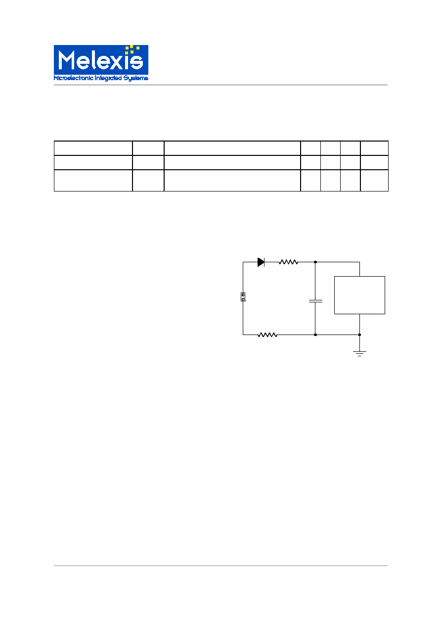
The MLX90719 supply pin (VDD4) must be connected
by external series resistor and rectifier diode to the
mains. An internal Zener function limits the voltage at
VDD4 to 70-80V. For proper operation, a decoupling
capacitor needs to be connected between VDD4 and
VSS (see figure 1).
90719
Vdd4
Vss
line
R1
R2
C
6k*
6k*
22uF*
*for information only
MLX90719
General purpose timer
3901090719
Page 4
Aug/02
Rev. 002
The MLX90719 has several internal supply lines for both analog and digital blocks:
Parameter
Symbol Test Conditions
Min Typ Max Units
Voltage applied at the supply pin
Vdd4
Idd4 = 5mA
DRAINB = Vss
63
73
77
V
Internal buzzer driver supply
Vbuz
Option OBZ3 active
20
V
Internal 11V supply
Vdd2
10
15
12
V
Internal 5V for main oscillator
Vdd1
4.5
5.0
5.5
V
Internal 5V for digital
Vdd
Normal mode
4.0
5.0
6.0
V
Low power mode
2.7
LCD driver supply
Vlcd
Option OLCD1 active
3.0
V
Option OLCD2 active
3.25
V
Option OLCD3 active
3.5
V
Option OLCD4 active
3.75
V
Option OLCD5 active
4
V
Option OLCD6 active
4.25
V
Option OLCD7 active
4.5
V
Option OLCD8 active
4.75
V
Option OLCD9 active
5
V
Option OLCD10 active
5.25
V
Option OLCD11 active
5.5
V
Option OLCD12 active
5.75
V
Option OLCD13 active
6
V
Option OLCD14 active
6.25
V
1Vlcd/3
Vlcd1
Of Vlcd
30
33
36
%
2Vlcd/3
Vlcd2
Of Vlcd
64
67
70
%
Idd4
For Vdd4<Vaporl (LPM)
3
uA
For Vdd4 = 73V
5
mA
Voltage of backup battery
Vbat
2.7
3
3.3
V
Supply for external circuitry
Vext
At Iext = 2mA
3.9
5
V

MLX902xx Name of Sensor
Rev Y.X
22/Aug/98
Page 5
MLX90719
General purpose timer
3901090719
Page 5
Aug/02
Rev. 002
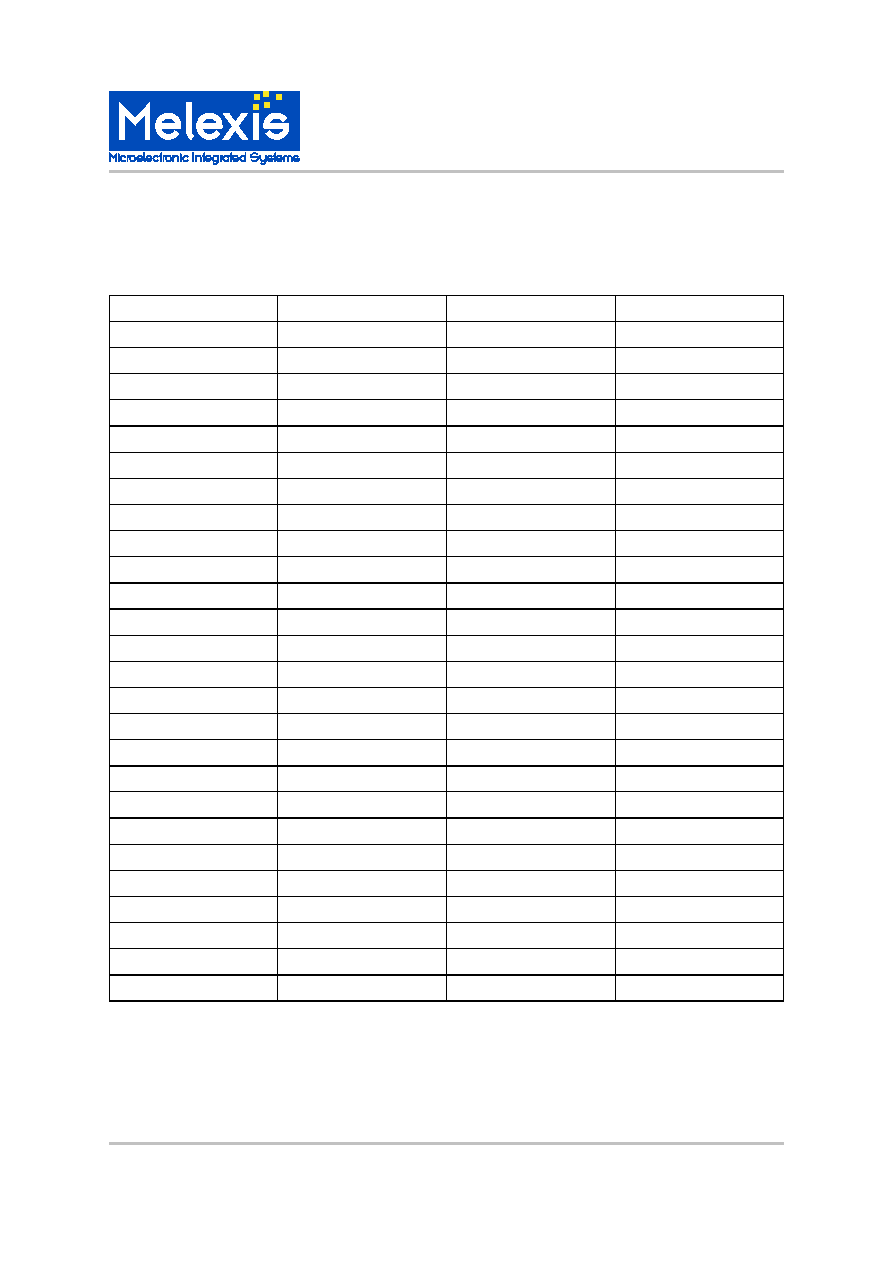
Parameter
Symbol Test Conditions
Min Typ Max Units
High level threshold
Vdporh
3.4
V
Low level threshold
Vdporl
2.2
2.6
V
Hysteresis
Vdphyst
0.3
V
Notes:
The power on reset does not reset the system when entering low power mode with battery (Vdporl<Vbat).
The power on reset resets the system if the RAM data may be corrupt due to undervoltage (Vdporl>RAM data
retention voltage).
Analog Power-On Reset
The MLX90719 includes a high voltage power-on reset that watches on VDD3.
This block has two outputs APORL and APORH:
APORL = 1 when VDD3 > Vaporl
APORH = 1 when VDD3 > Vaporh (see table 4)
The states of APORH and APORL define the operation mode of the chip (see sections "Sleep manager" and
"Interrupt controller").
In low power mode the analog power on reset operates in strobe mode. It is only enabled a few microseconds at
each rising edge of the signal ASTR generated by the digital core.
When Vdd3 > Vaporl the circuit goes out of strobe mode.
Parameter
Symbol Test Conditions
Min Typ Max Units
High level threshold
Vaporh
65
V
Low level threshold
Vaporl
50
V
Hysteresis
Vaphyst
10
V
Strobe frequency
Fastr
Slow rate of Vdd3>200V/s
25
Hz
Low power mode (LPM)
In low power mode (when the mains have been disconnected from the application) all supply lines are disabled
except VDD, which is generated by a low consuming regulator. The current is taken from the external decoup-
ling capacitor of VDD4 or from a backup battery connected to pin BAT. This depends on the type of application
defined by the mask option OXBAT implemented within the chip:
OXBAT = 1 for application with battery and crystal.
OXBAT = 0 for applications without battery or crystal.
LCD operating voltage
The LCD operating voltage can have14 different values and can be chosen by mask options.
Supply for external components
If the mask option OVEXT is set the MLX90719 can supply some external circuitry from the internal Vdd1
through pin IN5B (which can not be used as input anymore).
Power On Reset
This module ensures a correct start of the MLX90719 logic.
The reset signal (DPORB) rises when VDD>Vdporh and falls when VDD<Vdporl

MLX90719
General purpose timer
3901090719
Page 6
Aug/02
Rev. 002
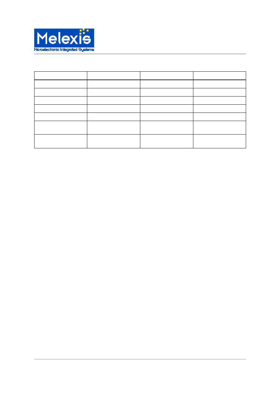
Zero crossing detector
The MLX90719 includes a zero crossing detector on pin ZCD. This detector contains two comparators with hys-
teresis. The first comparator has negative thresholds and the second one has positive thresholds (see table 5).
Outputs ZOUT1 and ZOUT2 of those comparators are changing as follows:
ZOUT1 rises when Vmains>Vz1h
ZOUT1 falls when Vmains<Vz1l
ZOUT2 rises when Vmains>Vz2h
ZOUT2 falls when Vmains<Vz2l
A mask option defines the levels of those thresholds. Low levels (+/- 5V, option OZCD = 0) are suitable for zero
crossing detection and high levels (+/- 20V, option OZCD = 1) for frequency detection with a better noise immu-
nity.
A 1M
resistor must be connected between pin ZCD and the mains.
Parameter
Symbol Test Conditions
Min Typ Max Units
High level threshold 1
Vz1h
Rzcd = 1Mohm
-5
V
Rzcd = 1Mohm, OZCD = 1
-5
V
Low level threshold 1
Vz1l
Rzcd = 1Mohm
-9
V
Rzcd = 1Mohm, OZCD = 1
-29
V
High level threshold 2
Vz2h
Rzcd = 1Mohm
9
V
Rzcd = 1Mohm, OZCD = 1
29
V
Low level threshold 2
Vz2l
Rzcd = 1Mohm
5
V
Rzcd = 1Mohm, OZCD = 1
5
V
External resistor
Rzcd
Vline = 230VAC typical
0.8
1
1.2
Mohm
Low voltage inputs
The MLX90719 has 7 CMOS Schmitt trigger inputs with internal pull-up.
Note: the input signals are inverted in the digital core so these inputs are active low.
Signal ENINB (active at 0) enables the pull-up current flowing through external pad to VSS if the input is pushed
to VSS. When ENINB=1 (input disabled), DINxB = 1.
The programmer must enable inputs by setting bit ENIN of P7 at least 5us before reading the input port P3 (see
section "I/O ports"). The debouncing of inputs must be done by software.
Parameter
Symbol Test Conditions
Min Typ Max Units
Pull-up current
Ipu1
Input to Vss
40
70
100 uA
Low level threshold
Vthinl
30
%Vdd
High level threshold
Vthinh
70
%Vdd
Hysteresis
Vhystin
5
%Vdd
Multipurpose inputs:
Inputs 3 and 6 can be used also as pull-down outputs: the pull down transistors are turned on by setting bits
PD3 and PD6 of P6 (see section "I/O ports").
Inputs 1, 2 and 4 are used by the on-chip comparator (see section "comparator")
Input 5 can be turned into supply for external circuitry by mask option OVEXT (see "Power supply").

MLX902xx Name of Sensor
Rev Y.X
22/Aug/98
Page 7
MLX90719
General purpose timer
3901090719
Page 7
Aug/02
Rev. 002
High voltage input
The MLX90719 has an eighth input that can be used either as a standard input (as described above) or as an
high voltage input to detect the mains via an external resistor. The high voltage mode is enabled if mask option
OIN7 is set.
Output DIN7B of this detector is high when Vmains>Vthinh2 and low when Vmains<Vthinl2.
Note: signal DIN7B is inverted whitin the digital core.
Parameter
Symbol Test Conditions
Min
Typ
Max Units
Pull-down current
Ipd2
12
uA
Low level threshold
Vthinl2
Rin = 1Mohm
6.9
V
High level threshold
Vthinh2 Rin = 1Mohm
12.3
V
External resistor
Rin
0.8
1
1.2
Mohm
Main oscillator
The MLX90719 contains a 4Mhz on-chip oscillator.
In low power mode this oscillator is turned off.
Parameter
Symbol Test Conditions
Min
Typ
Max Units
Master frequency of the
main oscillator (signal
CKM)
Fckm
Over full temp. and supply range
2.4
4.0
5.6
MHz
Low power crystal oscillator
In case of applications with battery and crystal (OXBAT = 1) the MLX90719 uses a low power crystal oscillator
as time reference for both normal and low power mode.
This oscillator requires a standard 32kHz crystal connected between pin XTAL1 and pin XTAL2.
No external capacitor is required for proper operation.
Parameter
Symbol Test Conditions
Min
Typ
Max Units
Master frequency of the
crystal oscillator
Fckx
Over full temp. and supply range
32768
Hz
Note: This oscillator is disabled if OXBAT = 0.
VDD
INxB
ENINB
DINxB

MLX90719
General purpose timer
3901090719
Page 8
Aug/02
Rev. 002
Low power RC oscillator
In case of applications without battery or crystal (OXBAT = 0) the MLX90719 uses an on-chip low power RC os-
cillator to count time during a few minutes after the mains has been disconnected (low power mode).
Parameter
Symbol Test Conditions
Min Typ Max Units
Master frequency of the
low power RC oscillator
Fckl
Over full temp. and supply range
1.0
2.5
5
kHz
Notes:
As the CPU must calibrate it in normal mode, the low power oscillator is running continuously.
The low power RC oscillator is disabled if OXBAT = 1.
LCD outputs
The MLX90719 has 15 configurable LCD outputs able to drive either a backplane or a segment by mask option:
OLCDx = 0 => segment
OLCDx = 1 => backplane
The LCD voltages are defined according to bits LCDx and CKLCD written in P3 and P4 (see section "I/O
ports"). With Vcdl1 and Vlcd2 being respectively 1/3Vlcd and 2/3Vlcd, the MLX90719 is suitable for LCD having
1, 2, 3 or 4 backplanes.
Parameter
Symbol Test Conditions
Min Typ Max Units
Output impedance
Rolcd
All cases
20
kohm
OLCDx
LCDx
CKLCD
OUT
0
0
0
Vlcd1
0
0
1
Vlcd2
0
1
0
Vlcd
0
1
1
Vss
1
0
0
Vlcd2
1
0
1
Vlcd1
1
1
0
Vss
1
1
1
Vlcd
Relay drivers
The MLX90719 includes 3 pull-down power outputs A, B, and C able to drive relays, triacs or LED's.
The gates of the drivers are controlled respectively by signals POUTA, POUTB and POUTC generated by the
digital core (see section "PWM generator").
Each driver has its source and its drain connected to a pad (DRAINx and SOURCEx) except driver C of which
the source is connected to the ground. This allows a series connection of the drivers. In such a configuration
the current flowing through the relay is used to feed the LED's.
Internal current generator
In applications based on the following schematic, where the LED(`s) may have to be driven when the relay is
off, an internal current peak generator can be activated to supply the LED's through pin SourceA. This function
is enabled by bit INTCUR of P5 (see section "I/O ports"). When INTCUR is set the current generator is acti-
vated like a relay by signal PINT at frequency Fpwm and at 14.3% duty cycle (see "PWM generator").
Note: If the application has no relay, this feature allows the MLX90719 to drive 2 LED's without any external
resistors.

MLX902xx Name of Sensor
Rev Y.X
22/Aug/98
Page 9
MLX90719
General purpose timer
3901090719
Page 9
Aug/02
Rev. 002
Parameter
Symbol Test Conditions
Min Typ Max Units
Ron of driver A
RonA
Source A pushed to VSS
10
30
W
Ron of driver B
RonB
Source B pushed to VSS
10
30
W
Ron of driver C
RonC
10
30
W
Voltage on pin DrainA
Vda
85
V
Voltage on pin DrainB
Vdb
85
V
Voltage on pin DrainC
Vdc
85
V
Voltage on pin SourceA
Vsa
8
V
Voltage on pin SourceB
Vsb
4
V
Rising edge duration, all
drivers
Tr
Load = 5k from VDD4 = 70V
1
us
Falling edge duration, all
drivers
Tf
Load = 5k from VDD4 = 70V
1
us
VDD4
90719
DrainA
SourceA
DrainB
SourceB
DrainC
RELAY
LED1
LED2
8V
Current
gen.
PINT
MLX90719
General purpose timer
3901090719
Page 10
Aug/02
Rev. 002
Buzzer driver
The MLX90719 includes a piezo buzzer driver.
The push-pull output stage of this driver operates at 15V. An internal resistor between the output pin and the
push-pull stage protects the chip against reverse piezo effect.
Parameter
Symbol Test Conditions
Min Typ Max Units
Output impedance
Rob
100 300 600 ohm
Maximum output frequency Fbuzm
8
kHz
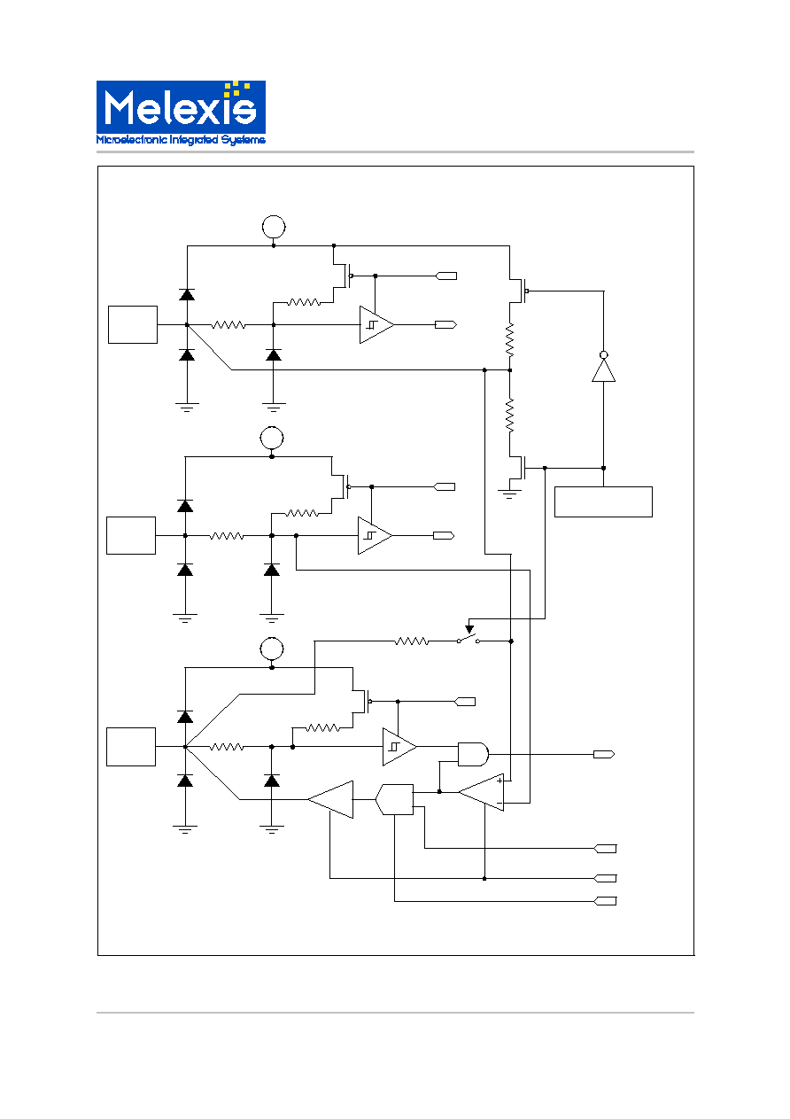
Comparator
The MLX90719 includes a multi-purpose comparator.
Setting bit ECOMP of P3 (see section "I/O ports") enables this comparator. Inputs IN1B and IN2B become re-
spectively the positive and negative inputs of the comparator and IN4B becomes its output via a tri-state buffer.
To reduce the number of external components in applications using the comparator, a resistive bridge and a
feed back resistor (both internal) can be connected on the positive input of the comparator by mask option
OCOMP.
Notes:
Some logic in the digital core ensures that ENIN12B and ENIN4B = 1 when ECOMP = 1.
When ECOMP = 0 the comparator output is fixed to "1".
A programmable prescaler has been implemented to allow frequency measurement at the output of the com-
parator (line IN4B). The status of bits CM0 and CM1 of P3 define the prescale ratio as described in table 15:
electrical characteristics of the comparator.
Parameter
Symbol Test Conditions
Min Typ Max Units
Common mode range
Vcm
20
80
%Vdd
Offset
Vcoff
-30
30
mV
CM1
CM0
Divide ratio
0
0
Prescaler bypassed
0
1
/16
1
0
/32
1
1
/64
MLX902xx Name of Sensor
Rev Y.X
22/Aug/98
Page 11
MLX90719
General purpose timer
3901090719
Page 11
Aug/02
Rev. 002
Tri state
COMP
R
R
OCOMP
ECOMP
A
SA
CKM*
CTST*
(* reserved for test)
R
VDD
IN1B
ENIN12B
VDD
IN2B
ENIN12B
VDD
IN4B
ENIN4B
DIN1B
DIN4B
DIN2B

MLX90719
General purpose timer
3901090719
Page 12
Aug/02
Rev. 002
Digital features
I/O ports
The MLX90719 has 9 port addresses. Read and write instructions to the same address do not access to the
same port:
Note: * = reserved for test.
Note: * = reserved for test.
Out Description
Msb
Lsb
P0 Timer compare low
TCP7
TCP6
TCP5
TCP4 TCP3
TCP2
TCP1
TCP0
P1 Timer compare high
TCP15
TCP14 TCP13 TCP12 TCP11
TCP10
TCP9
TCP8
P2 Timer ctrl, comparator
CM1
CM0
ECOMP TRST COUNT EN24H
MUX1
MUX0
P3 LCD port
LCD8
LCD9
LCD10 LCD11 LCD12
LCD13
LCD14
LCD15
P4 LCD port
CKLCDB LCD1
LCD2
LCD3 LCD4
LCD5
LCD6
LCD7
P5 Power outputs
Not used INTCUR PC1
PC0
PB1
PB0
PA1
PA0
P6 PWM frequency adjust
PD6
PD3
DIV5
DIV4 DIV3
DIV2
DIV1
DIV0
P7 IT control, sleep, wdog
PWD
RSTWD FLAG
ENIN RFHIT
ETIMI
ECLKI
ESUPI
P8 Sound, test
CTST*
DTST*
MTST* LTST* SOUND3 SOUND2 SOUND1
SOUND0
in
Description
Msb
Lsb
P0 Timer low
T7
T6
T5
T4
T3
T2
T1
T0
P1 Timer high
T15
T14
T13
T12
T11
T10
T9
T8
P2 Timer msb, test
BATB*
X*
X*
X*
X*
X*
X*
T16
P3 Chip inputs
IN7
IN6
IN5
IN4
IN3
IN2
IN1
IN0
P4 Not used
X
P5 Not used
X
P6 Not used
X
P7 IT handler, flag
ZCD
0
FLAG
0
0
PTIMI
PCLKI
PSUPI
P8 Not used
X
MLX902xx Name of Sensor
Rev Y.X
22/Aug/98
Page 13
MLX90719
General purpose timer
3901090719
Page 13
Aug/02
Rev. 002
Sleep manager and watch dog
At power-on-reset the MLX90719 is in low power mode (PWD = 1).
When VDD3 reaches 65V (APORH = 1) PWD is reset and the main oscillator starts. To ensure a correct start of
the analog blocks, the CPU is kept in reset status for 2
15
main clock pulses (typically 8.2ms).
Once the microcontroller is working a watchdog circuitry will generate a system reset if the user program fails to
reset the watchdog counter. The watchdog delay is given by:
Twd = 57344 x 1/Fckm (= 14ms if Fckm = 4MHz)
The watchdog counter is reset each time a 1 is written on bit RSTWD of P7.
To distinguish a wake-up after power-on reset and a wake-up after low power mode, one can read the status of
bit FLAG (read/write bit in P7). This will be 0 after power on reset and 1 after low power mode if FLAG has been
set during normal mode.
The low power mode is set by bit PWD of P7. Since the main oscillator stops as soon as PWD = 1, setting bit
PWD must be the last instruction of the supply interrupt subroutine (see interrupt controller).
Debouncing
A debounce circuit eliminates positive spikes on line APORH to avoid unexpected wake-up due to distur-
bances. The debounce time (tdaporh) depends on OXBAT.
If OXBAT = 1 it derives from the crystal oscillator frequency and:
7.8ms < tdaporh < 11.7ms
If OXBAT = 0 it derives from the low power RC oscillator frequency and:
3.2ms < tdaporl < 24ms
Timer
The MLX90719 includes a 17-bit timer preceded by a 15-bit prescaler. The clock of the timer can be taken from
four different sources defined by the bits MUX0 and MUX1 of P2:
The battery and crystal option (OXBAT) defines which clock is connected to the prescaler input:
If OXBAT =1: the crystal oscillator output (CKX) drives the prescaler input
If OXBAT = 0: the low power RC oscillator output (CKL) drives the prescaler input.
Control bits (P2):
EN24H = 1 enables the 24h mode (see below).
COUNT = 1 enables the counter
TRST = 1 resets the counter and the prescaler.
Normal operation
In normal mode the timer is used as a free-running counter on CK125K. It can be read at any time without stop.
An interrupt is generated when the value of the timer reaches the value of the timer compare written in P1-P0.
Low power mode if crystal oscillator (OXBAT = 1)
In this mode the clock of the timer must be connected to the /2
15
output of the prescaler (1Hz).
Setting the 24h mode turns the timer into a modulo 86400 counter if a correct value has been written in P1-P0.
The timer being automatically reset when T16=1 and T[15:0] = TCP[15:0], this value must be 517Fh to give T
[16:0] = 86399.
MUX1
MUX0
Timer clock source
Description
0
0
CK125K
Main clock divided by 32 (typically 125kHz)
0
1
D2P15
/2
15
prescale output
1
0
D2P9
/2
9
prescale output
1
1
D2P3
/2
3
prescale output

MLX90719
General purpose timer
3901090719
Page 14
Aug/02
Rev. 002
At wake-up the value of the timer is the number of seconds passed since the beginning of sleep. An arbitrary
time of 0.5s should be added to this number to compensate the error of 0/- 1s due to the timer resolution.
Low power mode without crystal oscillator (OXBAT = 0)
In this mode the timer clock must be connected to the /2
9
output of the prescaler (about 5Hz).
At wake up a calibration of the low power oscillator can be done by connecting the timer clock to the /2
3
output
of the prescaler and counting during 250ms (given by 25 half period of the mains at 50Hz and 30 half period at
60Hz).
Those prescale ratios allow a calibration of the low power oscillator with only one 16-bit division if its frequency
is in the range of 1-5kHz and if the maximum time to count is 5min.
Interrupt controller
The MLX8 core accepts only one interrupt source.
The MLX90719 has 3 interrupt sources:
Supply
Clock reference (crystal oscillator or zero crossing detector)
Timer
These three hardware parts will interrupt the MLX8 core to address 21h (interrupt address).
In order to recognize the interrupting device, an interrupt handler is readable at port P7 (bits PSUPI, PCLKI and
PTIMI). In case of interrupt:
PSUPI is set if the voltage on VDD3 has decreased under 50V (APORL=0)
PCLKI is set if a clock reference pulse has occurred.
PTIMI is set if the timer has reached the timer compare value (16-bit word in P0-P1).
Main program
IT
Read P7
PSUPI=1
PCLKI=1
PTIMI=1
Interrupt subroutine
....
Clear IT:
set & reset ECLKI
Interrupt subroutine
....
SLEEP
Interrupt subroutine
....
Clear IT:
set & reset ETIMI
Refresh IT controller :
set & reset RFHIT
Y
N
Y
N
N
Y
Y
N
At address 21h :
interrupt processing

MLX902xx Name of Sensor
Rev Y.X
22/Aug/98
Page 15
MLX90719
General purpose timer
3901090719
Page 15
Aug/02
Rev. 002
Option OXBAT defines which source generates the clock reference interrupt:
If OXBAT = 1 the clock interrupts are generated at the rate of 128Hz (Crystal frequency divided by 256).
If OXBAT = 0 the clock interrupts are generated at the rate of twice the mains frequency by the zero crossing
detector (combination of signals ZOUT1 and ZOUT2) that is 100Hz or 120Hz.
The main purpose of the timer interrupt is to rate the multiplexing of the LCD but it can be used to control a
triac.
Each interrupt can be enabled/disabled and cleared by setting or resetting ESUPI, ECLKI and ETIMI in P7.
As several interrupts may occur at the same time a fourth control bit RFHIT (of P7) has been implemented to
refresh the interrupt controller after each interrupt subroutine. The flow chart shows the interrupt process:
Debouncing
A debounce circuit eliminates negative spikes on line APORL to avoid unexpected supply interrupts due to dis-
turbances. The debounce time (tdaporl) depends on OXBAT.
If OXBAT = 1 it derives from the crystal oscillator frequency and:
7.8ms < tdaporl < 11.7ms
If OXBAT = 0 it derives from the low power RC oscillator frequency and:
3.2ms < tdaporl < 24ms
Both outputs of the zero crossing detector are combined in a debounce circuit that generates a periodic signal
rising at each zero crossing of the mains without delay. This signal (ZCD) is connected to the interrupt handler
(if OXBAT = 0) at bit PCLKI. The debounce period is typically 2ms but can vary from 0.6ms to 6ms because is it
generated from the low power RC oscillator.
Zero crossing signal on P7
The zero crossing signal is readable at bit ZCD of P7. This feature may be used to detect zero crossing in crys-
tal-based applications.
PWM generator
The three relay drivers of the MLX90719 can be driven independently at 0%, 14.3%, 28.6% and 100% duty
cycle (except driver A which can not be driven at 100% duty).
Bits PA0 to PC1 of P5 set the duty cycle of each driver (signals POUTA, POUTB and POUTC) and bit INTCUR
activates the current peak generator (signal PINT):
Note: * = 0% for driver A
t30 is given by: tclki < t30 < 2tclki
where tclki is the delay between two clock interrupts:
tclki = 10ms if zero crossing detector is used and Fmains = 50Hz
tclki = 8.33ms if zero crossing detector is used and Fmains = 60Hz
tclki = 7.81ms if crystal oscillator is used
In all cases: 7.81ms < t30 < 15ms
INTCUR
Px1
Px0
Duty cycle of
Duty cycle of
X
0
0
0 %
X
0
1
14.3 %
X
1
0
100 % *
X
1
1
28.6 % for t30 then
14.3%
0
X
X
0 %
1
X
X
14.3%

MLX90719
General purpose timer
3901090719
Page 16
Aug/02
Rev. 002
The PWM frequency is programmable. It depends on the main oscillator frequency and on the 6-bit divide ratio
written in P6:
Fpwm = Fckm /(7 x DIV[6:0]) (= 22kHz for Fckm = 4MHz and DIV[6:0] = 26)
As Fckm can vary, the divide ratio must be calculated periodically by software to reference Fpwm to the crystal
frequency or to the mains frequency.
Sound generator
The MLX90719 includes a sound generator able to produce more than 8 tonalities.
The output frequency Fbuz is defined by bits SOUND3 to SOUND0 of P3:
Fbuz = (7 x Fpwm) / (8 x S) (see table 21)
Mask options
The following table lists all options of the MLX90719 chip:
SOUND3
SOUND2
SOUND1
SOUND0
S
Fbuz if Fpwm = 22kHz
0
0
0
0
-
Off
0
0
0
1
2
(9.62kHz)
0
0
1
0
3
6.42kHz
0
0
1
1
4
4.81kHz
0
1
0
0
5
3.85kHz
0
1
0
1
6
3.21kHz
0
1
1
0
7
2.75kHz
0
1
1
1
8
2.41kHz
1
0
0
0
9
2.14kHz
1
0
0
1
10
1.93kHz
1
0
1
0
11
(1.75kHz)
1
0
1
1
12
(1.60kHz)
1
1
0
0
13
(1.48kHz)
1
1
0
1
14
(1.38kHz)
1
1
1
0
15
(1.28kHz)
1
1
1
1
16
(1.20kHz)
MLX902xx Name of Sensor
Rev Y.X
22/Aug/98
Page 17
MLX90719
General purpose timer
3901090719
Page 17
Aug/02
Rev. 002
Name
Value = 0
Value = 1
Bit*
OXBAT
No battery, no crystal
Battery + crystal
0
OVLCD1
Vlcd = 3V
1
OVLCD2
Vlcd = 3.25V
2
OVLCD3
Vlcd = 3.5V
3
OVLCD4
Vlcd = 3.75V
4
OVLCD5
Vlcd = 4V
5
OVLCD6
Vlcd = 4.25V
6
OVLCD7
Vlcd = 4.5V
7
OVLCD8
Vlcd = 4.75V
8
OVLCD9
Vlcd = 5V
9
OVLCD10
Vlcd = 5.25V
10
OVLCD11
Vlcd = 5.5V
11
OVLCD12
Vlcd = 5.75V
12
OVLCD13
Vlcd = 6V
13
OVLCD14
Vlcd = 6.25V
14
OVEXT
No external 5V supply
External 5V supply on IN5B
15
OZCD
Low thresholds
High thresholds
16
OIN7
Low voltage
High voltage
17
OCOMP
Bridge + feedback disabled
Bridge + feedback enabled
18
OLCD1
LCD1 = segment
LCD1 = backplane
19
OLCD2
LCD2 = segment
LCD2 = backplane
20
OLCD3
LCD3 = segment
LCD3 = backplane
21
OLCD4
LCD4 = segment
LCD4 = backplane
22
OLCD5
LCD5 = segment
LCD5 = backplane
23
OLCD6
LCD6 = segment
LCD6 = backplane
24
OLCD7
LCD7 = segment
LCD7 = backplane
25
OLCD8
LCD8 = segment
LCD8 = backplane
26
OLCD9
LCD9 = segment
LCD9 = backplane
27
OLCD10
LCD10 = segment
LCD10 = backplane
28
OLCD11
LCD11 = segment
LCD11 = backplane
29
OLCD12
LCD12 = segment
LCD12 = backplane
30
OLCD13
LCD13 = segment
LCD13 = backplane
31
OLCD14
LCD14 = segment
LCD14 = backplane
32
OLCD15
LCD15 = segment
LCD15 = backplane
33
* Only applicable for the development version of the MLX90719
MLX90719
General purpose timer
3901090719
Page 18
Aug/02
Rev. 002
Name
Num. (CCW)
Description
Options
LCD15
18
LCD14
19
LCD13
20
LCD12
21
LCD11
22
LCD10
23
LCD9
24
LCD8
25
LCD7
26
LCD6
27
LCD5
28
LCD4
29
LCD3
30
LCD2
31
LCD1
32
XTAL1
33
XTAL2
34
BAT
35
Battery pin
IN0B
36
Input 0
IN1B
1
Input 1
Comparator "+"
IN2B
2
Input 2
Comparator "-"
IN3B
3
Input 3
BUZ
4
Buzzer output
VSS
5
Vss
DRAINC
6
Drain of driver C
SOURCEB
7
Source of driver B
DRAINB
8
Drain of driver B
Pinout
Package type: SSOP36
MLX902xx Name of Sensor
Rev Y.X
22/Aug/98
Page 19
MLX90719
General purpose timer
3901090719
Page 19
Aug/02
Rev. 002
Name
Num. (CCW)
Description
Options
SOURCEA
9
Source of driver A
DRAINA
10
Drain of driver A
VDD4
11
Supply pin
IN4B
12
Input 4
Comparator output
IN5B
13
Input 5
Vext
IN6B
14
Input 6
IN7B
15
Input 7 (with high voltage
capability)
ZCD
16
Main frequency detector
input

MLX90719
General purpose timer
3901090719
Page 20
Aug/02
Rev. 002
Development board
Melexis has available a development kit which contains a evaluation circuit board, a ROM emulator, interface
cables, all necessary software and a sample of the MLX90917 (development version). The evaluation board is
a standard version that can be customized to an extended range of applications. The standard version includes
a buzzer, a LCD, a relay and some breadboard space to build up the customized application. (push buttons,
high-power outputs, temperature measurement, ...) The available software consists of assembler, linker, simu-
lator and the interface software for the ROM emulator. By using this emulator the user is able to see and modify
all internal registers and the RAM contents. On a break event, the user program is replaced by a shadow moni-
tor, which exchanges data with the host.
For software development a special version of the MLX90917 is available. This version differs from the stan-
dard MLX90917 in two ways. It has a second ring of pads around the normal chip. In this way the chip can be
used with external memory, which makes it also possible to use the ROM emulator. With the development ver-
sion it is also possible to program the different `mask' options. The state of the different options should be writ-
ten by the programmer in specific ROM bytes. During the initialization phase of the chip, a dedicated part in the
software reads this bytes and writes the contents in specific memory elements, defining in this way the chosen
options.
More information about the development board and software can be found in the specific documentation de-
scribing the MLX90719 Development Kit.

MLX902xx Name of Sensor
Rev Y.X
22/Aug/98
Page 21
MLX90719
General purpose timer
3901090719
Page 21
Aug/02
Rev. 002
Application Example
MLX90719
LCD 13
LCD 12
LCD 11
LCD 10
LCD 9
LCD 8
LCD 7
LCD 6
LCD 5
LCD 4
LCD 3
LCD 2
LCD 1
LCD
13
BUZ
DC
SB
DB
SA
DA
Relay
IN0B
IN1B
IN2B
IN3B
IN4B
IN5B
IN6B
IN7B
XTAL1
XTAL2
Thermal Switch
BAT
VDD4
VSS
MAINS
SW1
SW2
SW3
SW4
SW5
SW6
Pot.
Rref
Cap
Decoupling
Cap

MLX90719
General purpose timer
3901090719
Page 22
Aug/02
Rev. 002
Related documents
MLX90719 application note: a clock timer based on
the MLX90719.
LX11 simulator documentation:
http://www.melexis.com/site/know-how/mcu/tools/
mcu_tools_softsimul.htm.
MLX90719 development kit documentation:
describes how to define an application with the
MLX90719.
MLX902xx Name of Sensor
Rev Y.X
22/Aug/98
Page 23
MLX90719
General purpose timer
3901090719
Page 23
Aug/02
Rev. 002
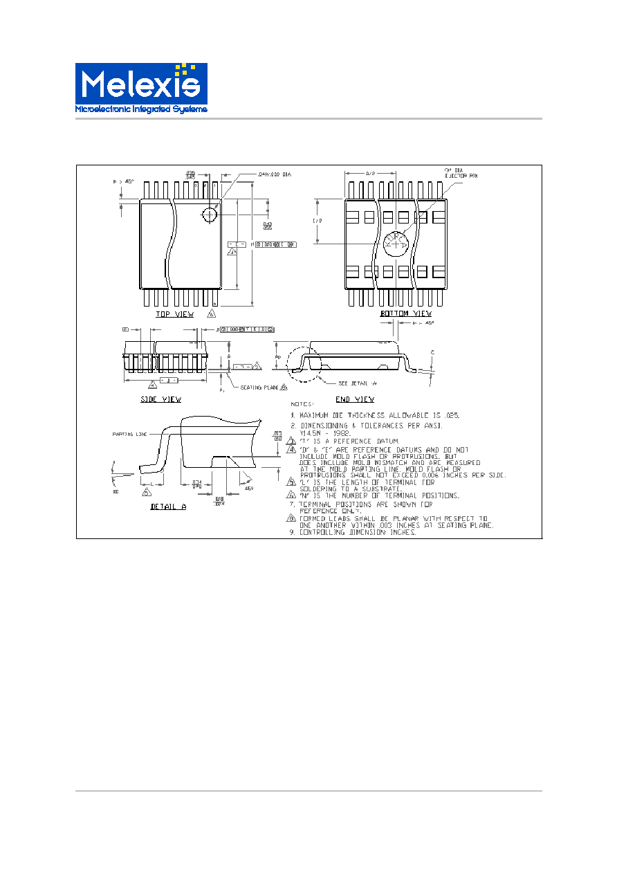
DF (SOIC 16, 300mil) Package Information

MLX90719
General purpose timer
3901090719
Page 24
Aug/02
Rev. 002
Reliability Information
Melexis devices are classified and qualified regarding suitability for infrared, vapor phase and
wave soldering with usual (63/37 SnPb-) solder (melting point at 183degC).
The following test methods are applied:
IPC/JEDEC J-STD-020A (issue April 1999)
Moisture/Reflow Sensitivity Classification For Nonhermetic Solid State Surface Mount Devices
CECC00802 (issue 1994)
Standard Method For The Specification of Surface Mounting Components (SMDs) of Assessed
Quality
MIL 883 Method 2003 / JEDEC-STD-22 Test Method B102
Solderability
For all soldering technologies deviating from above mentioned standard conditions (regarding
peak temperature, temperature gradient, temperature profile etc) additional classification and
qualification tests have to be agreed upon with Melexis.
The application of Wave Soldering for SMD's is allowed only after consulting Melexis regarding
assurance of adhesive strength between device and board.
For more information on manufacturability/solderability see quality page at our website:
http://www.melexis.com/
ESD Precautions
Electronic semiconductor products are sensitive to Electro Static Discharge (ESD).
Always observe Electro Static Discharge control procedures whenever handling semiconductor
products.

MLX902xx Name of Sensor
Rev Y.X
22/Aug/98
Page 25
MLX90719
General purpose timer
3901090719
Page 25
Aug/02
Rev. 002
Disclaimer
Devices sold by Melexis are covered by the warranty and patent indemnification provisions appear-
ing in its Term of Sale. Melexis makes no warranty, express, statutory, implied, or by description re-
garding the information set forth herein or regarding the freedom of the described devices from pat-
ent infringement. Melexis reserves the right to change specifications and prices at any time and with-
out notice. Therefore, prior to designing this product into a system, it is necessary to check with
Melexis for current information. This product is intended for use in normal commercial applications.
Applications requiring extended temperature range, unusual environmental requirements, or high
reliability applications, such as military, medical life-support or life-sustaining equipment are specifi-
cally not recommended without additional processing by Melexis for each application.
The information furnished by Melexis is believed to be correct and accurate. However, Melexis shall
not be liable to recipient or any third party for any damages, including but not limited to personal in-
jury, property damage, loss of profits, loss of use, interrupt of business or indirect, special incidental
or consequential damages, of any kind, in connection with or arising out of the furnishing, perform-
ance or use of the technical data herein. No obligation or liability to recipient or any third party shall
arise or flow out of Melexis' rendering of technical or other services.
© 2002 Melexis NV. All rights reserved.
For the latest version of this document, go to our website at:
www.melexis.com
Or for additional information contact Melexis Direct:
Europe and Japan:
All other locations:
Phone: +32 13 67 04 95
Phone: +1 603 223 2362
E-mail: sales_europe@melexis.com
E-mail: sales_usa@melexis.com
QS9000, VDA6.1 and ISO14001 Certified