
TH71112
868/915MHz
FSK/FM/ASK Receiver
3901071112
Page 1 of 20
Data Sheet
Rev. 007
Feb./03
Features
!
Double superhet architecture for high degree of image rejection
!
FSK for digital data and FM reception for analog signal transmission
!
FSK/FM demodulation with phase-coincidence demodulator
!
Low current consumption in active mode and very low standby current
!
Switchable LNA gain for improved dynamic range
!
RSSI allows signal strength indication and ASK detection
!
Surface mount package LQFP32
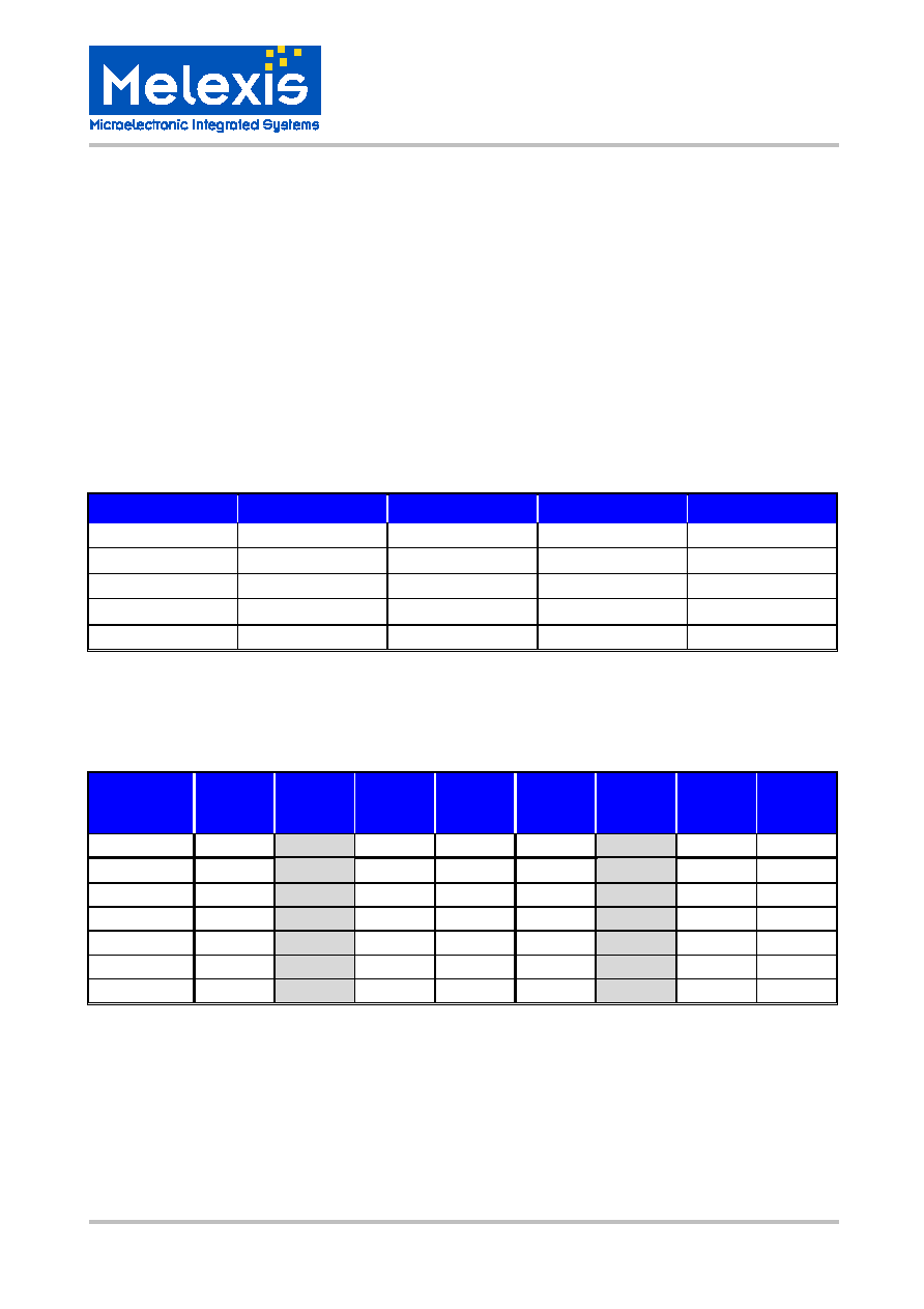
Ordering Information
Part No.
Temperature Code
Package Code
TH71112
E (-40 �C to 85 �C)
NE (LQFP32)
Application Examples
!
General digital and analog 800 MHz or
930 MHz ISM band usage
!
Low-power
telemetry
!
Alarm and security systems
!
Remote Keyless Entry (RKE)
!
Tire Pressure Monitoring System (TPMS)
!
Garage door openers
!
Home
automation
!
Pagers
Pin Description
General Description
The TH71112 FSK/FM/ASK double-conversion superheterodyne receiver IC is designed for applications in
the European 868 MHz industrial-scientific-medical (ISM) band, according to the EN 300 220 telecommuni-
cations standard. It can also be used for any other system with carrier frequencies ranging from 800 MHz to
930 MHz (e.g. for applications in the US 915 MHz ISM band).
V
EE_
L
N
AC
O
U
T
_LN
A
IN
_M
I
X
1
VEE_
M
I
X
I
F
_1P
IF
_
1
N
V
CC_
M
I
X
GA
I
N
_
L
N
A
VC
C
_
BI
AS
VEE_
BI
AS
OA
P
OA
N
OU
T
_
O
A
R
SSI
OU
T
P
VEE_RO
RO
ENRX
VEE_LNA
IN_LNA
VCC_LNA
LF
VCC_PLL
OUT_IFA
FBC1
FBC2
IN_IFA
VEE_IF
OUT_MIX2
VCC_IF
1
32
8
9
24
25
TH71112
17
16

TH71112
868/915MHz
FSK/FM/ASK Receiver
3901071112
Page 2 of 20
Data Sheet
Rev. 007
Feb./03
Document Content
1
Theory of Operation...................................................................................................3
1.1 General .............................................................................................................................. 3
1.2 Technical Data Overview ................................................................................................... 3
1.3 Block Diagram.................................................................................................................... 4
1.4 Mode Configurations .......................................................................................................... 4
1.5 LNA GAIN Control.............................................................................................................. 4
1.6 Frequency Planning ........................................................................................................... 5
1.6.1
Selected Frequency Plans ............................................................................................................5
2
Pin Definitions and Descriptions ..............................................................................6
3
Technical Data............................................................................................................9
3.1 Absolute Maximum Ratings................................................................................................ 9
3.2 Normal Operating Conditions ............................................................................................. 9
3.3 Crystal Parameters ............................................................................................................ 9
3.4 DC Characteristics ........................................................................................................... 10
3.5 AC System Characteristics .............................................................................................. 11
4
Test Circuits .............................................................................................................12
4.1 FSK Reception................................................................................................................. 12
4.2 FSK test circuit component list (Fig. 2)............................................................................. 13
4.3 FSK/FM Circuit with AFC and Ceramic Resonator Compensation ................................... 14
4.4 FSK/FM (with AFC) test circuit component list (Fig.3)...................................................... 15
4.5 ASK Reception................................................................................................................. 16
4.6 ASK Test Circuit Component List (Fig. 4)......................................................................... 17
5
Package Dimensions ...............................................................................................18
6
Reliability Information .............................................................................................19
7
ESD Precautions ......................................................................................................19
8
Disclaimer.................................................................................................................20

TH71112
868/915MHz
FSK/FM/ASK Receiver
3901071112
Page 3 of 20
Data Sheet
Rev. 007
Feb./03
1
Theory of Operation
1.1 General
With the TH71112 receiver chip, various circuit con-
figurations can be arranged in order to meet a num-
ber of different customer requirements. For FSK/FM
reception the IF tank used in the phase coincidence
demodulator can be constituted either by a ceramic
resonator or an LC tank (optionally with a varactor
diode to create an AFC circuit). In ASK configura-
tion, the RSSI signal is feed to an ASK detector,
which is constituted by the operational amplifier.
Demodulation
Type of receiver
FSK / FM
narrow-band RX with
ceramic demodulation tank
FSK / FM
wide-band RX with
LC demodulation tank
ASK
RX with RSSI-based demodulation
The superheterodyne configuration is double conversion where MIX1 and MIX2 are driven by the internal
local oscillator signals LO1 and LO2, respectively. This allows a high degree of image rejection, achieved in
conjunction with an RF frontend filter. Efficient RF front-end filtering is realized by using a SAW, ceramic or
helix filter in front of the LNA and by adding an LC filter at the LNA output.
A single-conversion variant, called TH71111, is also available. Both Receiver ICs have the same die. At the
TH71111 the second mixer MIX2 operates as an amplifier.
The TH71112 receiver IC consists of the following building blocks:
"
PLL synthesizer (PLL SYNTH) for generation of the first and second local oscillator signals LO1 and LO2
"
Parts of the PLL SYNTH are the high-frequency VCO1, the feedback dividers DIV_16 and DIV_2,
a phase-frequency detector (PFD) with charge pump (CP) and a crystal-based reference oscillator (RO)
"
Low-noise amplifier (LNA) for high-sensitivity RF signal reception
"
First mixer (MIX1) for down-conversion of the RF signal to the first IF (IF1)
"
Second mixer (MIX2) for down-conversion of the IF1 to the second IF (IF2)
"
IF amplifier (IFA) to amplify and limit the IF2 signal and for RSSI generation
"
Phase coincidence demodulator (DEMOD) with third mixer (MIX3) to demodulate the IF signal
"
Operational amplifier (OA) for data slicing, filtering and ASK detection
"
Bias circuitry for bandgap biasing and circuit shutdown
1.2 Technical Data Overview
!
Input frequency range: 800 MHz to 930 MHz
!
Power supply range: 2.3 V to 5.5 V @ ASK
!
Temperature range: -40 �C to +85 �C
!
Standby current: 50 nA
!
Operating current: 7.5 mA at low gain mode
9.2 mA at high gain mode
!
Sensitivity: -112 dBm
1)
with 40 kHz IF filter BW
!
Sensitivity: -105 dBm
2)
with 150 kHz IF filter BW
!
Range of first IF1: 10 MHz to 80 MHz
!
Range of second IF2: 400 kHz to 22 MHz
!
Maximum data rate: 80 kbit/s NRZ
!
Maximum input level: -10 dBm at ASK
0 dBm at FSK
!
Image rejection: > 65 dB (e.g. with SAW
front-end filter and at 10.7 MHz IF2)
!
Spurious emission: < -70 dBm
!
Input frequency acceptance:
�
50 kHz
(with AFC option)
!
RSSI range: 70 dB
!
Frequency deviation range:
�
4 kHz to
�
120 kHz
!
Maximum analog modulation frequency: 15 kHz
1) at
�
8 kHz FSK deviation, BER = 3
10
-3
and phase-coincidence demodulation
2) at
�
50 kHz FSK deviation, BER = 3
10
-3
and phase-coincidence demodulation

TH71112
868/915MHz
FSK/FM/ASK Receiver
3901071112
Page 4 of 20
Data Sheet
Rev. 007
Feb./03
1.3 Block
Diagram
Fig. 1:
TH71112 block diagram
1.4 Mode
Configurations
ENRX
Mode
Description
0
RX standby
RX disabled
1
RX active
RX enable
Note: ENRX are pulled down internally
1.5 LNA GAIN Control
V
GAIN_LNA
Mode
Description
< 0.8 V
HIGH GAIN
LNA set to high gain
> 1.4 V
LOW GAIN
LNA set to low gain
Note: hysteresis between gain modes to ensure stability
IN_LNA
LNA
MIX1
IFA
GA
I
N
_
L
N
A
O
U
T_
LN
A
FP
C
2
R
SSI
OU
T
_
I
F
A
IN
_
D
E
M
OUTP
OUTN
MIX3
21
9
3
2
31
1
VEE_
L
N
A
C
5
VEE_
MI
X
32
V
CC_
L
N
A
30
VEE_
L
N
A
IN
_
M
I
X
1
4
V
CC_M
I
X
8
13
15
16
RO
LF
26
VCO1
RO
PFD
29
24
23
VC
C
_
PL
L
27
BIAS
28
EN
R
X
17
VC
C
_
B
I
A
S
22
VEE_
B
I
A
S
25
VEE_
R
O
14
OU
T
_
M
I
X
2
IN
_
I
F
A
11
VEE_
I
F
10
FB
C
1
12
OAP
OAN
19
20
18
OUT_OA
OA
IF1
P
IF
1
N
7
6
MIX2
IF1
IF2
DIV_16
DIV_2
LO1
LO2
CP
TH71112
868/915MHz
FSK/FM/ASK Receiver
3901071112
Page 5 of 20
Data Sheet
Rev. 007
Feb./03
1.6 Frequency
Planning
Frequency planning is straightforward for single-conversion applications because there is only one IF that
might be chosen, and then the only possible choice is low-side or high-side injection of the LO signal (which
is now the one and only LO signal in the receiver).
The receiver's double-conversion architecture requires careful frequency planning. Besides the desired RF
input signal, there are a number of spurious signals that may cause an undesired response at the output.
Among them are the image of the RF signal (that must be suppressed by the RF front-end filter), spurious
signals injected to the first IF (IF1) and their images which could be mixed down to the same second IF (IF2)
as the desired RF signal (they must be suppressed by the LC filter at IF1 and/or by low-crosstalk design).
By configuring the TH71112 for double conversion and using its internal PLL synthesizer with fixed feedback
divider ratios of N1 = 16 (DIV_16) and N2 = 2 (DIV_2), four types of down-conversion are possible: low-side
injection of LO1 and LO2 (low-low), LO1 low-side and LO2 high-side (low-high), LO1 high-side and LO2
low-side (high-low) or LO1 and LO2 high-side (high-high). The following table summarizes some equations
that are useful to calculate the crystal reference frequency (REF), the first IF (IF1) and the VCO1 or first LO
frequency (LO1), respectively, for a given RF and second IF (IF2).
Injection type
high-high
low-low
high-low
low-high
REF
(RF � IF2)/30
(RF � IF2)/34
(RF + IF2)/30
(RF + IF2)/34
LO1
32
�
REF
32
�
REF
32
�
REF
32
�
REF
IF1
LO1 � RF
RF � LO1
LO1 � RF
RF � LO1
LO2
2
�
REF
2
�
REF
2
�
REF
2
�
REF
IF2
LO2 � IF1
IF1 � LO2
IF1 � LO2
LO2 � IF1
1.6.1 Selected Frequency Plans
The following table depicts crystal, LO and image signals considering the examples of 868.3 MHz and
915 MHz RF reception at IF2 = 10.7 MHz.
Signal type
RF =
868.3
MHz
RF =
868.3
MHz
RF =
868.3
MHz
RF =
868.3
MHz
RF =
915
MHz
RF =
915
MHz
RF =
915
MHz
RF =
915
MHz
Injection type
high-high
low-low
high-low
low-high
high-high
low-low
high-low
low-high
REF / MHz
28.58667
25.22353
29.3
25.85294
30.14333
26.59706
30.85667
27.22647
LO1 / MHz
914.77333 807.15294
937.6
827.29412 964.58667 851.10588 987.41333 871.24706
IF1 / MHz
46.47333
61.14706
69.3
41.00588
49.58667
63.89412
72.41333
43.75294
LO2 / MHz
57.17333
50.44706
58.6
51.70588
60.28667
53.19412
61.71333
54.45294
RF image/MHz 961.24667 746.00588
1006.9
786.28824
1014.17
787.21176
1059.83
827.49412
IF1 image/MHz
67.87333
39.74706
47.9
62.40588
70.98667
42.49412
51.01333
65.15294
The selection of the reference crystal frequency is based on some assumptions. As for example: the first IF
and the image frequencies should not be in a radio band where strong interfering signals might occur
(because they could represent parasitic receiving signals), the LO1 signal should be in the range of 800 MHz
to 930 MHz (because this is the optimum frequency range of the VCO1). Furthermore the first IF should be
as high as possible to achieve highest RF image rejection. The columns in bold depict the selected frequency
plans to receive at 868.3 MHz and 915 MHz, respectively.