 | –≠–ª–µ–∫—Ç—Ä–æ–Ω–Ω—ã–π –∫–æ–º–ø–æ–Ω–µ–Ω—Ç: TH8056 | –°–∫–∞—á–∞—Ç—å:  PDF PDF  ZIP ZIP |

TH8056
Enhanced Single Wire CAN Transceiver
TH8056
≠
Datasheet
Page
1
of
21
3901008056
June 2003
Rev 001b
Features
Features
Features
Features
Fully compatible with J2411 Single Wire CAN specification for Class B in vehicle
communications
30 µA typical power consumption in sleep mode independent from CAN voltage range
Operating voltage range 5V to 27V
Up to 40 kbps bus speed
Up to 100 kbps high-speed transmission mode
Logic inputs compatible with 3.3V and 5V supply systems
Control pin for external voltage regulators
Low RFI due to output wave shaping in normal and high speed wake up mode
Fully integrated receiver filter
Bus terminals proof against short-circuits and transients in automotive environment
Loss of ground protection
Protection against load dump, jump start
Thermal overload and short circuit protection
ESD protection of 4 kV on CAN pin (2kV on any other pin)
Undervoltage lock-out
Bus dominant timeout feature
14-pin thermally enhanced SOIC package
Ordering Information
Part
No.
Temperature
Range
Package
TH8056 KDC
K (-40 to 125 ∞C)
DC (SOIC14)
General Description
General Description
General Description
General Description
The TH8056 is a physical layer device for a single wire data link capable of operating with various CSMA/CR protocols
such as the Bosch Controller Area Network (CAN) version 2.0. This serial data link network is intended for use in
applications where a high data rate is not required and a lower data rate can achieve cost reductions in both the physical
media components and the microprocessor and/or dedicated logic devices which use the network.
The network shall be able to operate in either the normal data rate mode or the high speed data download mode for
assembly line and service data transfer operations. The high speed mode is only intended to be operational when the
bus is attached to an off-board service node. This node shall provide temporary bus electrical loads which facilitate
higher speed operation.
The bit rate for normal communications is typically 33.33kbit/s, for high speed transmissions like described above a
typical bit rate of 83.33kbit/s is recommended. The TH8056 is designed in accordance to the Single Wire CAN Physical
Layer Specification GMW3089 V2.1 and supports many additional features like undervoltage lockout, timeout for faulty
blocked
input signals, output blanking time in case of bus ringing and a very low sleep mode current.

TH8056
Enhanced Single Wire CAN Transceiver
TH8056
≠
Datasheet
Page
2
of
21
3901008056
June 2003
Rev 001b
Contents
1.
Functional Diagram ................................................................................................... 3
2.
Electrical Specification.............................................................................................. 4
2.1
Operating Conditions ............................................................................................ 4
2.2
Absolute Maximum Ratings .................................................................................. 4
2.3
Static Characteristics ............................................................................................ 5
2.4
Dynamic Characteristics ....................................................................................... 7
2.5
Bus loading requirements ..................................................................................... 8
2.6
Timing Diagrams................................................................................................... 9
3.
Functional Description ............................................................................................ 11
3.1
TxD Input pin ...................................................................................................... 11
3.2
Mode 0 and Mode 1 pins .................................................................................... 11
3.3
RxD Output pin ................................................................................................... 12
3.4
Bus LOAD pin ..................................................................................................... 12
3.5
V
bat
INPUT
pin................................................................................................... 13
3.6
CAN BUS pin ...................................................................................................... 13
3.7
INH Pin ............................................................................................................... 13
3.8
State Diagram..................................................................................................... 14
3.9
Application Circuitry ............................................................................................ 15
4.
Pin Description......................................................................................................... 16
5.
Package Dimensions ............................................................................................... 17
6.
Revision History....................................................................................................... 18
7.
Reliability Information ............................................................................................. 19
8.
ESD Precautions ...................................................................................................... 19
9.
Disclaimer................................................................................................................. 21
List of Figures
List of Figures
List of Figures
List of Figures
Figure 1 - Block Diagram ......................................................................................................................... 3
Figure 2 - Input / Output Timing............................................................................................................... 9
Figure 3 - Wakeup Filter Time Delay ..................................................................................................... 10
Figure 4 - Receive Blanking Time.......................................................................................................... 10
Figure 5 - Truth Table ............................................................................................................................ 11
Figure 6 - State Diagram........................................................................................................................ 14
Figure 7 - Application Circuitry............................................................................................................... 15

TH8056
Enhanced Single Wire CAN Transceiver
TH8056
≠
Datasheet
Page
3
of
21
3901008056
June 2003
Rev 001b
1.
1.
1.
1.
Functional Diagram
Functional Diagram
Functional Diagram
Functional Diagram
TxD
MODE0
RxD
CANH
MODE
CONTROL
MODE1
Time Out
Wave Shaping
CAN Driver
Reverse
Current
Protection
Biasing&
V
BAT
Monitor
V
BAT
5V Supply &
References
Reverse
Current
Protection
Feedback-
Loop
Loss of
Ground
Detection
Receive
Comparator
Input
Filter
RCOsc
TH8056
RxD Blanking
Time Filter
GND
LOAD
INH
Wake up filter
Figure 1 - Block Diagram

TH8056
Enhanced Single Wire CAN Transceiver
TH8056
≠
Datasheet
Page
4
of
21
3901008056
June 2003
Rev 001b
2.
2.
2.
2.
Electrical Specification
Electrical Specification
Electrical Specification
Electrical Specification
All voltages are referenced to ground (GND). Positive currents flow into the IC.
The absolute maximum ratings (in accordance with IEC 134) given in the table below are limiting values that
do not lead to a permanent damage of the device but exceeding any of these limits may do so. Long term
exposure to limiting values may affect the reliability of the device.
2.1 Operating
Conditions
Parameter
Symbol
Min
Max
Unit
Battery voltage
V
BAT
5.0
18
V
Operating ambient temperature
T
A
-40
125
∞C
Junction temperature
T
J
-40
150
∞C
2.2 Absolute Maximum Ratings
Parameter
Symbol
Condition
Min
Max
Unit
Supply Voltage
V
BAT
-0.3 18 V
Load dump; t<500ms
40
Short-term supply voltage
V
BAT.ld
Jump start; t<1min
27
V
Transient supply voltage
V
BAT.tr1
ISO 7637/1 pulse 1
[1]
-50
V
Transient supply voltage
V
BAT..tr2
ISO 7637/1 pulses 2
[1]
100
V
Transient supply voltage
V
BAT..tr3
ISO 7637/1 pulses 3A, 3B
-200
200
V
V
BAT
<= 27V
-20
40
CANH voltage
V
CANH
V
BAT
= 0
-40
40
V
Transient bus voltage
V
CANH..tr1
ISO 7637/1 pulse 1
[2]
-50
V
Transient bus voltage
V
CANH.tr2
ISO 7637/1 pulses 2
[2]
100
V
Transient bus voltage
V
CANH.tr3
ISO 7637/1 pulses 3A, 3B
[2]
-200 200 V
DC voltage on pin LOAD
V
LOAD
via R
T
> 2k
-40 40 V
DC voltage on pins TxD, MODE1, MODE0,RxD,
V
DC
-0.3 7 V
ESD capability of CANH
ESD
CANHB
Human body model,
equivalent to discharge
100pF with 1.5k
,
-4 4
kV
ESD capability of any other pins
ESD
HB
Human body model,
equivalent to discharge
100pF with 1.5k
,
-2 2
kV
Maximum latch ≠ up free current at any Pin
I
LATCH
-500 500 mA
Maximum power dissipation
P
tot
At
T
amb
= +125 ∞C
> 400
[3]
mW
Thermal impedance
JA
in free air
< 70
K/W
Storage temperature
T
stg
-55 150 ∞C
Junction temperature
T
vj
-40 150 ∞C
[1]
ISO 7637 test pulses are applied to VBAT via a reverse polarity diode and >1uF blocking capacitor .
[2]
ISO 7637 test pulses are applied to CANH via a coupling capacitance of 1 nF.
[3]
The application board shall be realized with a ground copper foil area >150mm
2

TH8056
Enhanced Single Wire CAN Transceiver
TH8056
≠
Datasheet
Page
5
of
21
3901008056
June 2003
Rev 001b
2.3 Static
Characteristics
Unless otherwise specified all values in the following tables are valid for V
BAT
= 5V to 27V and T
AMB
=-40∞C to
125
o
C. All voltages are referenced to ground (GND), positive currents are flow into the IC.
Parameter
Symbol
Condition
Min
Typ
Max
Unit
PIN VBAT
Operating supply voltage
V
BAT
5
12 18 V
Short duration Operating supply voltage
V
BAT_JS
T<1min,
T
amb
< 85∞C
18
27
V
Undervoltage lock-out
V
BATuv
4.3
4.8 V
Supply current, recessive, all active modes
I
BATN
V
BAT
= 18V , TxD open
3.5
5
mA
Normal mode supply current, dominant
I
BATN [2]
V
BAT
= 18V MODE0=MODE1=H
TxD=L, R
load
= 200
28
33
mA
High-speed mode supply current, dominant
I
BATN [2]
V
BAT
= 18V
MODE0=H,MODE1=L,TxD=L,
R
load
= 92
55 60
mA
Wake-up mode supply current, dominant
I
BATW [2]
V
BAT
= 18V
MODE0=L,MODE1=H, TxD=L,
R
load
= 200
59 65
mA
Sleep mode supply current
I
BATS
V
BAT
=18V, TxD, RxD, MODE0,
MODE1 open;
30 50
µA
PIN CANH
Bus output voltage
V
oh
R
L
> 92
,
Normal, high-speed mode,
5V < V
BAT
< 6V
3.4 5.1
V
Bus output voltage
V
oh
R
L
> 200
, Normal mode,
6V < V
BAT
< 27V
4.4 5.1
V
Bus output voltage
V
oh
R
L
> 92
, high-speed mode,
8V < V
BAT
< 18V
4.4 5.1
V
Fixed Wake-up Output High Voltage
V
ohWuFix
Wake-up mode, R
L
> 200
,
11.2V < V
BAT
< 27V
9.9 12.5
V
Offset Wake-up Output High Voltage
V
ohWuOffset
Wake-up mode, R
L
> 200
,
5.5V < V
BAT
< 11.2V
V
BAT
≠ 1.5
V
BAT
V
Recessive state output voltage
V
ol
Recessive state or sleep mode,
R
load
= 6.5
k
,
-0.2 0.20
V
Bus short circuit current
-I
CAN_SHORT
V
CANH
= 0V, V
BAT
= 27V,
TxD = 0V
50 150
mA
Bus leakage current during loss of ground
I
LKN_CAN[1]
Loss of ground, V
CANH
= 0V
-50
10
µA
Bus leakage current, bus positive
I
LKP_CAN
TxD high;
-10
10
µA
Bus input threshold
V
ih
Normal, high-speed mode
2.0
2.1
2.2
V
Bus input hysteresis
V
ihhys
Normal, high-speed mode
0.02
0.1
V
Fixed Wake-up Input High Voltage
Threshold
V
i
hWuFix
[2]
Sleep mode, V
BAT
> 11.2V
6.6
7.9
V
Offset Wake-up Input High Voltage
Threshold
V
ihWuOffset
[2]
Sleep mode
V
BAT
-4.3 V
BAT
-3.25 V

TH8056
Enhanced Single Wire CAN Transceiver
TH8056
≠
Datasheet
Page
6
of
21
3901008056
June 2003
Rev 001b
Parameter
Symbol
Condition
Min
Typ
Max
Unit
PIN LOAD
Voltage on switched ground pin
V
LOAD
I
RTH
= 5mA
0.5
V
Voltage on switched ground pin
V
LOAD_LOB
I
LOAD
= 7mA , V
BAT
= 0V
1
V
Load resistance during loss of battery
R
LOAD_LOB
V
BAT
= 0, R
LOAD
= 2K, V
CANH
= 5V
1.6K
2.4K
PIN TXD,MODE0,MODE1
High level input voltage
V
ih
2.0
V
Low level input voltage
V
il
0.8 V
TxD pull up current
-I
IL_TXD
TxD = L, MODE0 and 1 = H
20
50
µA
MODE pull down resistor
R
MODE_pd
20
40 k
PIN RXD
Low level output voltage
V
ol_rxd
I
RxD
= 2mA
0.4
V
High level output leakage
I
ih_rxd
V
RxD
= 5V
-10
10
µA
RxD output current
Irxd
V
RxD
= 5V
70
mA
PIN INH
High level output voltage
V
oh_INH
I
INH
= -180µA
V
S
-0.8V V
S
-0.5V V
Leakage current
I
INH_lk
Mode0/1 = L ,V
INH
= 0V
-5
5
µA
Overtemperature Protection
Thermal shutdown
T
sd [2]
155
180
∞C
Thermal recovery
T
rec [2]
126
150
∞C
[1]
Leakage current in case of Loss of ground is the summary of both currents I
LKN_CAN
and
I
LKN_LOAD
.
[2]
Thresholds
not tested in production, but characterized and guaranteed by design

TH8056
Enhanced Single Wire CAN Transceiver
TH8056
≠
Datasheet
Page
7
of
21
3901008056
June 2003
Rev 001b
2.4 Dynamic
Characteristics
Unless otherwise specified all values in the following table are valid for V
BAT
= 5V to 27V and T
AMB
= -40∞C to
125
o
C
Parameter
Symbol
Condition
Min
Typ
Max
Unit
Transmit delay in normal & wake up mode,
rising edge
t
Tr [1]
= 1µs/4µs ,
measured from
TXD=0.8V to V
CANH
=1V/3.7V
3 6.3
µs
Transmit delay in wake-up mode to V
ihWU
,
rising edge
t
TWUr [2]
= 1µs/4µs , measured from
TXD=0.8V to V
CANH
=1V/9.4V,
V
BAT
> 11.2V
3 18
µs
Transmit delay in normal mode,
falling edge
t
Tf [3]
= 1µs/ 4µs ,measured from
TXD=2V to V
CANH
=3.7V/1V
3 8.5
µs
Transmit delay in wake-up mode,
falling edge
t
TWU1f [3]
= 1µs/4µs ,measured from
TXD=2V to V
CANH
=3.7V/1V
3
13.7
µs
Transmit delay in high-speed mode,
rising edge
t
THSr [4]
= 1.5µs ,measured from
TXD=2.0V to V
CANH
=1V/3.7V,
8V < V
BAT
< 18V
0.1 1.5
µs
Transmit delay in high-speed mode,
falling edge
t
THS f[5]
= 1.5µs, measured from
TXD=0.8V to V
CANH
=3.7V/1V
8V < V
BAT
< 18V
0.1 3
µs
Receive delay , all active modes
t
DR [6]
CANH to RxD, measured
from V
CANH
=2.2V ,
RxD=H to L
0.3 1
µs
Receive delay , all active modes
t
RD [6]
CANH to RxD, measured
from V
CANH
=2.2V ,
RxD=L to H
0.3 1
µs
Input minimum pulse length, all active
modes
t
mpDR [6]
CANH to RxD, measured
from V
CANH
=2.2V ,
RxD=H to L
0.2 1
µs
Input minimum pulse length, all active
modes
t
mpRD
CANH to RxD, measured
from V
CANH
=2.2V, RxD=L to H
0.2 1
µs
Wake-up filter time delay
t
WUF
See diagrams, Figure 3
10
70
µs
Receive blanking time after
TxD L-H
transition
t
rb
See diagrams, Figure 4
0.5
6
µs
TxD time-out reaction time
t
tout
Normal and high speed mode
15
ms
TxD time-out reaction time
t
toutwu
Wake up mode
20
ms
Delay from Normal to High Speed/HVWU
Mode
t
dnhs
30 µs
Delay from High Speed /HVWU to Normal
Mode
t
dhsn
30 µs
Delay from Normal Mode to Standby
t
dsby
500 µs

TH8056
Enhanced Single Wire CAN Transceiver
TH8056
≠
Datasheet
Page
8
of
21
3901008056
June 2003
Rev 001b
Parameter
Symbol
Condition
Min
Typ
Max
Unit
Delay from Standby to Sleep Mode
t
dsleep
100 250 1000 ms
Delay from Sleep to normal Mode
t
dsnwu
50 µs
[1]
The maximum signal delay time for a bus rising edge is measured from V
cmos il
on the TxD input pin to the V
ihMax
+ V
g off
max
level on CANH at maximum network time constant , minimum signal delay time for a bus rising edge is measured from V
cmos ih
on the TxD input pin to 1V on CANH at minimum network time constant .These definitions are valid in both normal and HVWU
mode
[2]
The maximum signal delay time for a bus rising edge in HVWU mode is measured from V
cmos il
on the TxD input pin to the
V
ihWUMax
+ V
g off
max level on CANH at maximum network time constant , minimum signal delay time for a bus rising edge is
measured from V
cmos ih
on the TxD input pin to 1V on CANH at minimum network time constant
[3]
Maximum signal delay time for a bus falling edge is measured from V
cmos ih
on the TxD input pin to 1V on CANH at maximum
network time constant, minimum signal delay time for a bus falling edge is measured from V
cmos ih
on the TxD input pin to the
V
ihMax
+ V
g off
max level on CANH. These definitions are valid in both normal and HVWU mode .
[4]
The signal delay time in high speed mode for a bus rising edge is measured from V
cmos il
on the TxD input pin to the V
ihMax
+ V
g
off
max level on CANH at maximum high speed network time constant
[5]
The signal delay time in high speed mode for a bus falling edge is measured from V
cmos ih
on the TxD input pin to 1V on CANH
at maximum high speed network time constant
[6]
Receive delay time is measured from the rising / falling edge crossing of the nominal Vih value on CANH to the falling
(Vcmos_il_max) / rising (Vcmos_ih_min) edge of RxD. This parameter is tested by applying a square wave signal to CANH.
The minimum slew rate for the bus rising and falling edges is 50V/us. The low level on bus is always 0V. For normal mode
and high-speed mode testing the high level on bus is 4V. For HVWU mode testing the high level on bus is Vbat ≠ 2V.
2.5 Bus loading requirements
Parameter
Symbol
Min
Typ
Max
Unit
Number of system nodes
2
32
Network distance between any two ECU nodes
Bus length
60
m
Node Series Inductor Resistance (if required)
R
ind
6 Ohm
Ground Offset Voltage
V
goff
1.5 V
Device Capacitance (unit load)
C
ul
198 220 300 pF
Network Total Capacitance
C
tl
396 19000 pF
Device Resistance (unit load)
R
ul
6435 6490 6565 Ohm
Device Resistance (min load)
R
min
2000
Ohm
Network Total Resistance
R
tl
200 4596 Ohm
High-Speed Mode Network Resistance to GND
R
load
92 185 Ohm
Network Time Constant
[1]
1 4 µs
Network Time Constant, high-speed mode
[1]
1.5
µs
[1]
The network time constant incorporates the bus wiring capacitance. The minimum value is selected to limit radiated emissions. The
maximum value is selected to ensure proper communication under all communication modes. Not all combinations of R and C are
possible. The network time constants are applied as follows:
= 1µs 2 KOhm/510pF,
= 4µs 210 Ohm/19nF,
= 1.5µs 92 Ohm/16.8nF (high speed mode)
TH8056
Enhanced Single Wire CAN Transceiver
TH8056
≠
Datasheet
Page
9
of
21
3901008056
June 2003
Rev 001b
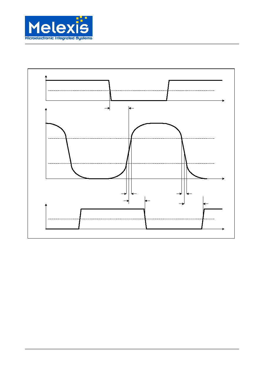
2.6 Timing
Diagrams
t
T
V
RxD
V
CANH
V
TxD
30%
70%
t
D
t
DR
50%
50%
t
R
t
F
t
t
t
Figure 2 - Input / Output Timing

TH8056
Enhanced Single Wire CAN Transceiver
TH8056
≠
Datasheet
Page
10
of
21
3901008056
June 2003
Rev 001b
V
RxD
V
CANH
t
WU
t
t
V
ih
+V
goff
t
WU
< t
WuF
t
Wu
t
WuF
wake up
interrupt
Figure 3 ≠ Wake-up Filter Time Delay
V
RxD
V
CANH
V
TxD
V
ih
t
rb
50%
t
t
t
50%
Figure 4 - Receive Blanking Time
TH8056
Enhanced Single Wire CAN Transceiver
TH8056
≠
Datasheet
Page
11
of
21
3901008056
June 2003
Rev 001b
3.
3.
3.
3.
Functional Description
Functional Description
Functional Description
Functional Description
3.1 TxD Input pin
Logic command to transmit on the single wire CAN bus
TxD Polarity
TxD = logic 1 (or floating) on this pin produces an undriven or recessive bus state (low bus voltage)
TxD = logic 0 on this pin produces either a bus normal or a bus high voltage dominant state
depending on the transceiver mode state (high bus voltage)
If the TxD pin is driven to a logic low state while Mode 0,1 pins are in the 0,0 or sleep state, the transceiver
cannot drive the CAN Bus pin to the dominant state.
The transceiver provides an internal pull up on the TxD pin, which will cause the transmitter to default to the
bus recessive state, when TxD is not driven.
TxD input signals are standard CMOS logic levels for 3.3V and 5V supply voltages.
Timeout feature
In case of a faulty blocked dominant TxD input signal the CANH output is switched off automatically after the
specified TxD timeout reaction time to prevent a dominant bus. The transmission is continued by next TxD L
to H transition without delay.
3.2 Mode 0 and Mode 1 pins
Select transceiver operating modes
The transceiver provides a weak internal pull down current on each of these pins, which causes the
transceiver to default to sleep mode when they are not driven. The Mode input signals are standard CMOS
logic level for 3.3V and 5V supply voltages.
M0
M1
Mode
L L
Sleep
Mode
H L
High-Speed
L H
High
Voltage
Wake-Up
H H
Normal
Mode
Figure 5 - Truth Table
Mode 0 = 0, Mode 1 = 0 - Sleep mode
Transceiver is in low power state, waiting for wake-up via high voltage signal or by mode pins change to any
state other than 0,0. In this state, the CAN Bus pin is not in the dominant state regardless of the state of the
TxD pin.
Mode 0 = 1, Mode 1 = 0 ≠ High-Speed mode
This mode allows high-speed download with bitrates up to 100Kbit/s. The output waveshaping circuit is
disabled in this mode. Bus transmitters which require communicating in high speed mode are able to drive
reduced bus resistance during this mode.

TH8056
Enhanced Single Wire CAN Transceiver
TH8056
≠
Datasheet
Page
12
of
21
3901008056
June 2003
Rev 001b
Mode 0 = 0, Mode 1 = 1 - Transmit with high voltage signals to wake up remote nodes (HVWU)
This bus includes a selective node awake capability, which allows normal communication to take place
among some nodes while leaving the other nodes in an undisturbed sleep state. This is accomplished by
controlling the signal voltages such that all nodes must wake up when they receive a higher voltage
message signal waveform. The communication system communicates to the nodes information as to which
nodes are to stay operational (awake) and which nodes are to put themselves into a non_communicating low
power "sleep" state. Communication at the lower, normal voltage levels does not disturb the sleeping nodes.
Mode 0 = 1, Mode 1 = 1 - Normal speed and signal voltage mode
Transmission bit rate in normal communication is 33.333 Kbits/sec. In normal transmission mode the
TH8056 supports controlled waveform rise and overshoot times. Waveform trailing edge control is required
to assure that high frequency components are minimized at the beginning of the downward voltage slope.
The remaining fall time occurs after the bus is inactive with drivers off and is determined by the RC time
constant of the total bus load.
3.3 RxD Output pin
Logic data as sensed on the single wire CAN bus
RxD polarity
RxD = logic 1 on this pin indicates a bus recessive state (low bus voltage)
RxD = logic 0 on this pin indicates a bus normal or high-voltage bus dominant state
RxD in Sleep Mode
RxD does not pass signals to the micro processor while in sleep mode until a valid wake up bus voltage level
is received or the Mode 0, 1 pins are not 0,0 respectively. When the valid wake-up bus signal awakens the
transceiver, the RxD pin signalises an interrupt (logic 0 for dominant high-voltage signal). If there is no mode
change within the time stated (typically 250ms), the transceiver reenters the sleep mode as described in 3.7
When not in sleep mode all valid bus signals will be sent out on the RxD pin.
RxD Typical Load
Resistance: 2.7 kohms
Capacitance: < 25 pF
3.4 Bus LOAD pin
Resistor ground with internal open-on-loss-of-ground protection
When the ECU experiences a loss of ground condition, this pin is switched to a high impedance state.
The ground connection through this pin is not interrupted in any transceiver operating mode including the
sleep mode. The ground connection only is interrupted when there is a valid loss of ground condition.
This pin provides the bus load resistor with a path to ground which contributes less than 0.1 volts to the bus
offset voltage when sinking the maximum current through one unit load resistor.
The transceiver's maximum bus leakage current contribution to V
ol
from the LOAD pin when in a loss of
ground state is 50 uA over all operating temperatures and 3.5 V < V
batt
< 27 V.

TH8056
Enhanced Single Wire CAN Transceiver
TH8056
≠
Datasheet
Page
13
of
21
3901008056
June 2003
Rev 001b
3.5 V
bat
INPUT
pin
Vehicle Battery Voltage
The transceiver is fully operational as described in chapter 2 over the range 5V<V
batt IC
<18V as measured
between the GND pin and this pin.
For 5V < V
batt IC
< 6V the bus operates in all active modes with reduced dominant output voltage. High
voltage wake-up call is not possible (dominant output voltage is the same as in normal or high-speed mode).
The transceiver operates in normal mode when 18V < V
batt IC
< 27V at 85∞C for one minute.
For 0V< V
bat IC
< 4.8V, the bus is passive (not driven dominantly) and RxD is undriven (high), regardless of
the state of the TxD pin (undervoltage lockout).
3.6 CAN
BUS
pin
Bus Input/Output
Wave Shaping in normal and HVWU mode
Wave shaping is incorporated into the transmitter to minimize EMI radiated emissions. An important
contributor to emissions is the rise and fall times during output transitions at the "corners" of the voltage
waveform. The resultant waveform is one half of a sine wave of frequency 50 - 65 kHz at the rising waveform
edge and one quarter of this sine wave at falling or trailing edge.
Short circuits
If the CAN BUS pin is shorted to ground for any duration of time, the current is limited to the specified value,
until an over temperature shut down circuit disables the output high side drive source transistor (before the
local die temperature exceeds the damage limit threshold).
Loss of ground
In case of an ECU loss of ground condition, the LOAD pin is switched into high impedance state. The CANH
transmission is continued until the undervoltage lock out voltage threshold is detected.
Loss of battery
In case of loss of battery (VBAT = 0 or open) the transceiver does not disturb bus communication. The
maximum reverse current into power supply system doesn't exceed 500µA.
3.7 INH
Pin
This Pin is a high voltage highside switch used to control the ECU's regulated microcontroller voltage supply.
After power-on the transceiver automatically enters an intermediate standby mode, the INH output will
become HIGH (VBAT) and therefore the external voltage regulator will provide the Vcc supply for the ECU .
If there is no mode change within the time stated (typically 250ms), the transceiver reenters the sleep mode
and the INH output goes to logic 0 (floating). When the transceiver has detected a valid wake-up condition
(bus HVWU traffic which exceeds the wake-up filter time delay) the INH output will become HIGH (VBAT)
again and the same procedure starts as described after power-on. In case of a mode change into any active
mode the sleep timer is stopped and INH keeps high (VBAT) level. If the transceiver enters the sleep mode
(M0,1=0), INH goes to logic 0 (floating) no sooner than typically 250ms when no wake-up signal is present .
TH8056
Enhanced Single Wire CAN Transceiver
TH8056
≠
Datasheet
Page
14
of
21
3901008056
June 2003
Rev 001b
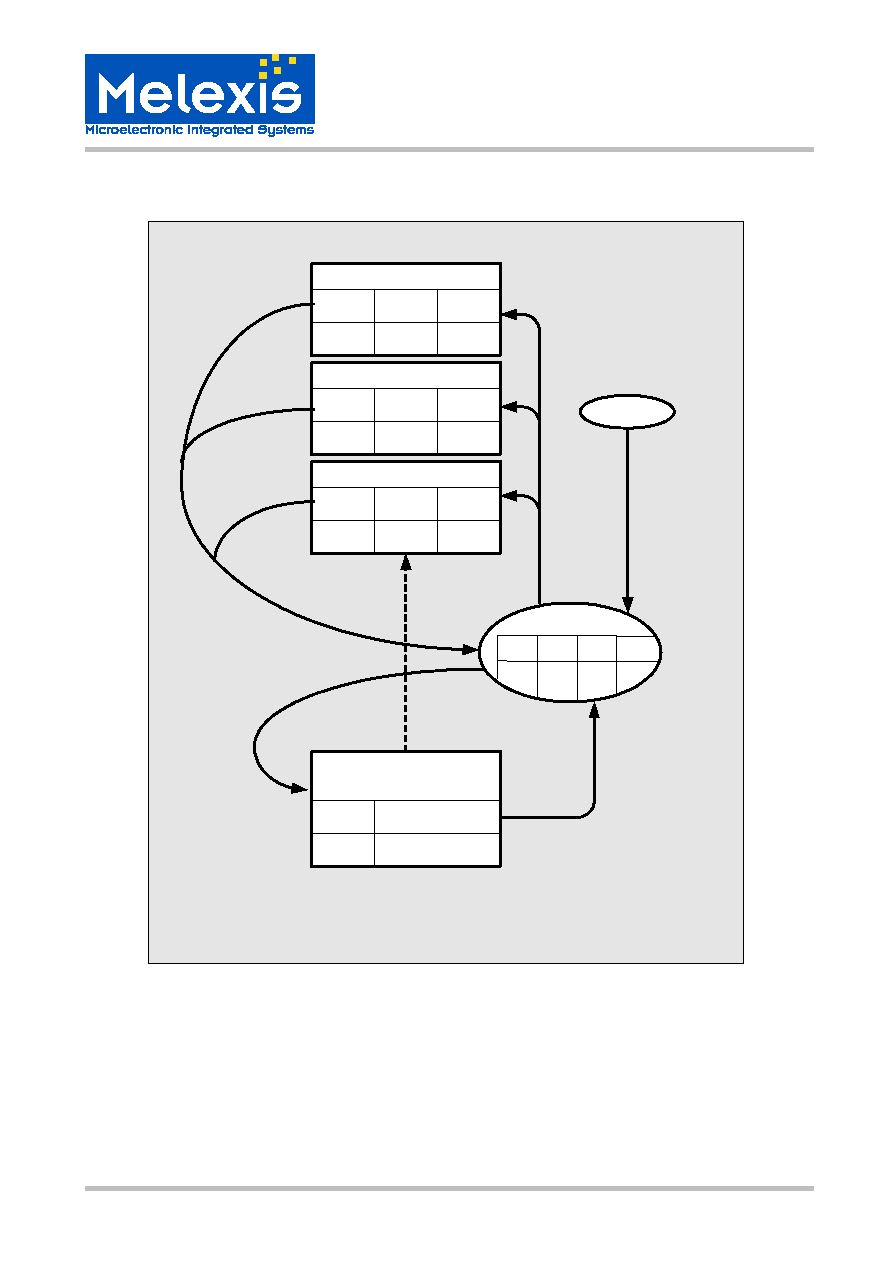
3.8 State
Diagram
Sleep Mode
M0/1
INH/CAN
low
floating
V
BAT
on
V
BAT
standby
M0&1=>Low
M0/1 =>High
wake up
request
from Bus
M0/1 =>High
(if V
CC_ECU
on)
[1]
low after HVWU, high after V
BAT
on & V
CCECU
present
INH
low
M0/1
V
S
low
[1]
RxD
high /
Normal Mode
M0
INH
high
V
BAT
M1
high
High Speed Mode
M0
INH
high
V
BAT
M1
low
HVWU Mode
M0
INH
low
V
BAT
M1
high
CAN
float.
after 250ms
-> no mode change
-> no valid wake up
Figure 6 - State Diagram

TH8056
Enhanced Single Wire CAN Transceiver
TH8056
≠
Datasheet
Page
15
of
21
3901008056
June 2003
Rev 001b
3.9 Application
Circuitry
100nF
TxD
TH8056
RxD
MODE0
MODE1
V
BAT
Voltage regulator
+5V
V
BAT
ECU connector to
Single Wire CAN Bus
LOAD
CANH
GND
VBAT
47µH
6.49kOhm
220pF
2.7kOhm
Copper Foil
Heat Sink
>150mm
2
ESD Protection -
TPSMA16A or
MMBZ27VCLT1 or
equivalent - if needed
10
11
12
5
3
4
2
1,7,8,14
V
BAT_ECU
[1]
[1] recommended capacitance at VBAT_ECU > 1uF (immunity to ISO7637/1 test pulses)
9
INH
other loads
Figure 7 - Application Circuitry

TH8056
Enhanced Single Wire CAN Transceiver
TH8056
≠
Datasheet
Page
16
of
21
3901008056
June 2003
Rev 001b
4.
4.
4.
4.
Pin Description
Pin Description
Pin Description
Pin Description
TH8056
1
2
3
4
8
TxD
VBAT
RXD
MODE0
GND
CANH
LOAD
MODE1
7
6
5
9
10
11
12
13
14
GND
GND
GND
INH
N.C.
N.C.
Pin
Name
IO-Typ
Description
1 GND P
Ground
2
TXD
I
Transmit data from MCU to CAN
3
MODE0
I
Operating mode select input 0
4
MODE1
I
Operating mode select input 1
5
RXD
O
Receive data from CAN to MCU
6 N.C.
7 GND P
Ground
8 GND P
Ground
9
INH
O
Control Pin for external voltage regulator (high voltage high side switch)
10
VBAT
P
Battery voltage
11
LOAD
O
Resistor load (loss of ground low side switch )
12
CANH
I/O
Single wire CAN bus pin
13 N.C.
14 GND P
Ground

TH8056
Enhanced Single Wire CAN Transceiver
TH8056
≠
Datasheet
Page
17
of
21
3901008056
June 2003
Rev 001b
5.
5.
5.
5.
Package Dimension
Package Dimension
Package Dimension
Package Dimensionssss
Small Outline Integrated Circiut (SOIC), SOIC 14, 150 mil
A1
B
C
D
E
e
H
h
L
A
ZD
A2
All Dimension in mm, coplanarity < 0.1 mm
min
max
0.10
0.25
0.36
0.45
0.19
0.25
8.56
8.74
3.81
3.99
1.27
5.80
6.20
0.25
0.50
0.41
1.27
1.52
1.72
0∞
8∞
0.51
1.37
1.57
All Dimension in inch, coplanarity < 0.004"
min
max
0.004
0.01
0.014
0.018
0.0075
0.0098
0.337
0.344
0.160
0.167
0.050 0.228
0.244
0.010
0.020
0.016
0.050
0.060
0.068
0∞
8∞
0.020 0.054
0.062

TH8056
Enhanced Single Wire CAN Transceiver
TH8056
≠
Datasheet
Page
18
of
21
3901008056
June 2003
Rev 001b
6.
6.
6.
6.
Revision History
Revision History
Revision History
Revision History
Version
Changes
Remark
Date
001
Initial
Release Sep.
2002
001a
-
Added chapter revision history
-
Error corrected within Figure 1 - Block Diagram
March
2003
001b
-
Pinout corrected within Figure 7 - Application Circuitry
06/13/03

TH8056
Enhanced Single Wire CAN Transceiver
TH8056
≠
Datasheet
Page
19
of
21
3901008056
June 2003
Rev 001b
7.
7.
7.
7.
Reliability Information
Reliability Information
Reliability Information
Reliability Information
Melexis devices are classified and qualified regarding suitability for infrared, vapor phase and wave soldering
with usual (63/37 SnPb-) solder (melting point at 183degC).
The following test methods are applied:
IPC/JEDEC J-STD-020A (issue April 1999)
Moisture/Reflow Sensitivity Classification For Nonhermetic Solid State Surface Mount Devices
CECC00802 (issue 1994)
Standard Method For The Specification of Surface Mounting Components (SMDs) of Assessed Quality
MIL 883 Method 2003 / JEDEC-STD-22 Test Method B102
Solderability
For all soldering technologies deviating from above mentioned standard conditions (regarding peak
temperature, temperature gradient, temperature profile etc) additional classification and qualification tests
have to be agreed upon with Melexis.
The application of Wave Soldering for SMD's is allowed only after consulting Melexis regarding assurance of
adhesive strength between device and board.
For more information on manufacturability/solderability see quality page at our website:
http://www.melexis.com/
8.
8.
8.
8.
ESD Precautions
ESD Precautions
ESD Precautions
ESD Precautions
Electronic semiconductor products are sensitive to Electro Static Discharge (ESD).
Always observe Electro Static Discharge control procedures whenever handling semiconductor products.

TH8056
Enhanced Single Wire CAN Transceiver
TH8056
≠
Datasheet
Page
20
of
21
3901008056
June 2003
Rev 001b
Your notes
Your notes
Your notes
Your notes

TH8056
Enhanced Single Wire CAN Transceiver
TH8056
≠
Datasheet
Page
21
of
21
3901008056
June 2003
Rev 001b
9.
9.
9.
9.
Disclaimer
Disclaimer
Disclaimer
Disclaimer
Devices sold by Melexis are covered by the warranty and patent indemnification provisions appearing in its
Term of Sale. Melexis makes no warranty, express, statutory, implied, or by description regarding the
information set forth herein or regarding the freedom of the described devices from patent infringement.
Melexis reserves the right to change specifications and prices at any time and without notice. Therefore,
prior to designing this product into a system, it is necessary to check with Melexis for current information.
This product is intended for use in normal commercial applications. Applications requiring extended
temperature range, unusual environmental requirements, or high reliability applications, such as military,
medical life-support or life-sustaining equipment are specifically not recommended without additional
processing by Melexis for each application.
The information furnished by Melexis is believed to be correct and accurate. However, Melexis shall not be
liable to recipient or any third party for any damages, including but not limited to personal injury, property
damage, loss of profits, loss of use, interrupt of business or indirect, special incidental or consequential
damages, of any kind, in connection with or arising out of the furnishing, performance or use of the technical
data herein. No obligation or liability to recipient or any third party shall arise or flow out of Melexis' rendering
of technical or other services.
© 2002 Melexis NV. All rights reserved.
For the latest version of this document. Go to our website at
www.melexis.com
Or for additional information contact Melexis Direct:
Europe and Japan:
All other locations:
Phone: +32 1367 0495
Phone: +1 603 223 2362
E-mail: sales_europe@melexis.com
E-mail: sales_usa@melexis.com
QS9000, VDA6.1 and ISO14001 Certified