3901001881
Page 1
Aug/02
Rev. 012
Features and Benefits
n
Chopper stabilized amplifier stage
n
Optimized for BDC motor applications
n
New miniature package / thin, high reliability package
n
Operation down to 3.5V
n
CMOS for optimum stability, quality and cost
Applications
n
Solid state switch
n
Brushless DC motor commutation
n
Speed sensing
n
Linear position sensing
n
Angular position sensing
n
Current sensing
Ordering Information
Part No.
Temperature Suffix
Package
US1881
E ( -40
o
C to 85
o
C )
SO (SOT-23) or UA (TO-92 flat)
US1881
L ( -40
o
C to 150
o
C )
SO (SOT-23) or UA (TO-92 flat)
*Contact factory or sales representative for legacy temperature options
Description
The US1881 is the industry's first Hall integrated
circuit in a SOT-23 package. The US1881 is a
bipolar Hall effect sensor IC fabricated from mixed
signal CMOS technology. It incorporates advanced
chopper stabilization techniques to provide accurate
and stable magnetic switch points. There are many
applications for this HED in addition to those listed
above. The design, specifications and performance
have been optimized for commutation applications in
5V and 12V brushless DC motors.
The output transistor will be latched on (B
OP
) in the
presence of a sufficiently strong South pole
magnetic field facing the marked side of the
package. Similarly, the output will be latched off
(B
RP
) in the presence of a North field.
The SOT-23 device is reversed from the UA
package. The SOT-23 output transistor will be
latched on in the presence of a sufficiently strong
North pole magnetic field applied to the marked
face.
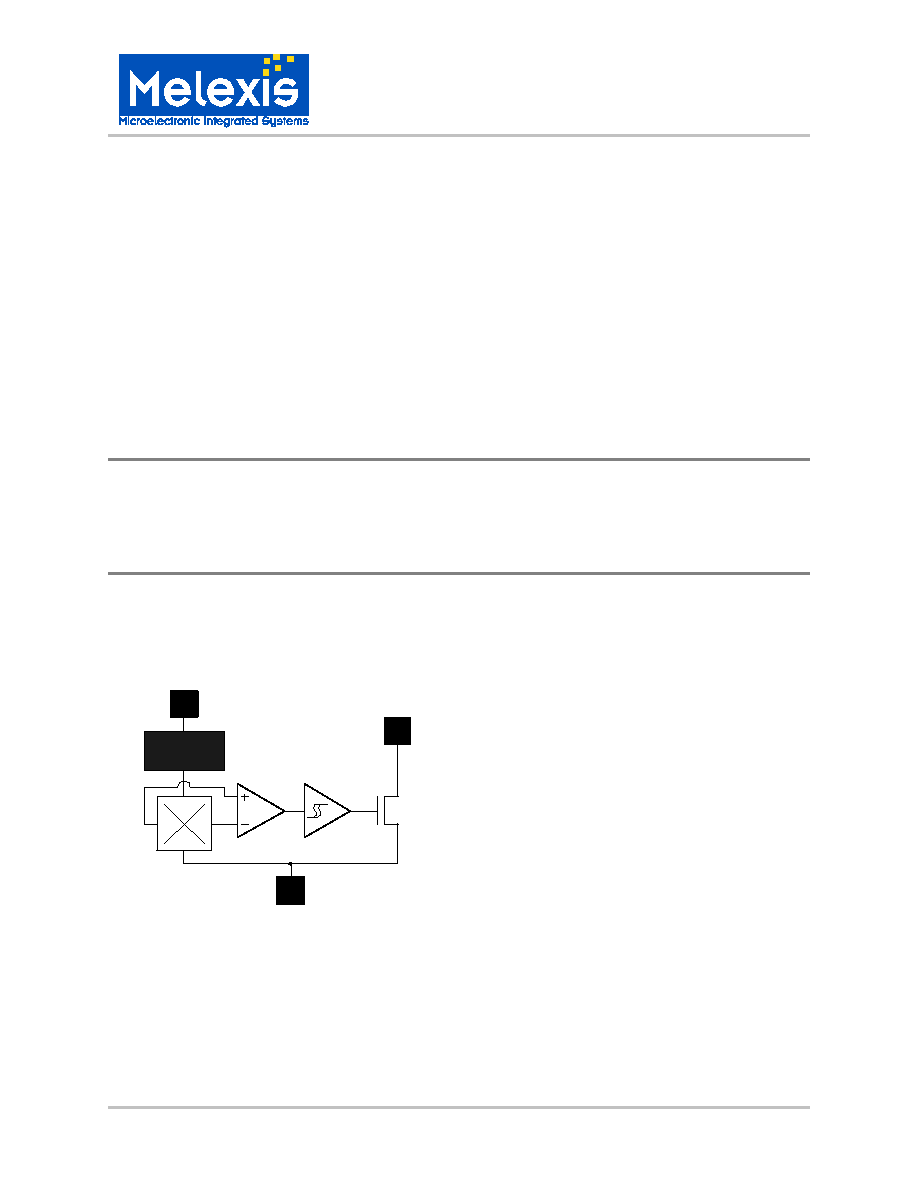
Functional Diagram
Note: Static sensitive device; please observe ESD precautions.
Reverse V
DD
protection is not included. For reverse voltage
protection, a 100W resistor in series with V
DD
is recommended.
Output
GND
V
DD
Voltage
Regulator
Chopper
SO Package
Pin 1 - V
DD
Pin 2 - Output
Pin 3 - GND
UA Package
Pin 1 - V
DD
Pin 2 - GND
Pin 3 - Output

3901001881
Page 2
Aug/02
Rev. 012
US1881 Electrical Specifications
DC Operating Parameters: T
A
= 25, V
DD
= 12V
DC
(unless otherwise specified).
Parameter
Symbol Test Conditions
Min
Typ
Max
Units
Supply Voltage
V
DD
Operating
3.5
24
V
Supply Current
I
DD
B<B
OP
1.1
2.5
5.0
mA
Saturation Voltage
V
DS(on)
I
OUT
= 20 mA, B>B
OP
0.4
0.5
V
Output Leakage
I
OFF
B<B
RP
, V
OUT
= 24V
0.01
10.0
A
Output Rise Time
t
r
V
DD
= 12V, R
L
= 1.1K
�
, C
L
= 20pf
0.04
s
Output Fall Time
t
f
V
DD
= 12V, R
L
= 1.1K
�
, C
L
= 20pf
0.18
s
US1881 Magnetic Specifications
Parameter
Symbol
Test Conditions
Min
Typ
Max
Units
Operating Point
B
OP
EUA,ESO,LUA,LSO 25�C, Vdd=3.5 & 24 volts DC
1.0
5.0
9.0
mT
Release Point
B
RP
EUA,ESO,LUA,LSO 25�C, Vdd=3.5 & 24 volts DC
-9.0
-5.0
-1.0
mT
Hysteresis
B
hys
EUA,ESO,LUA,LSO 25�C, Vdd=3.5 & 24 volts DC
7.0
10.0
12.0
mT
Operating Point
B
OP
EUA, ESO 85�C, Vdd=3.5 & 24 volts DC
0.5
5.0
9.5
mT
Release Point
B
RP
EUA, ESO 85�C, Vdd=3.5 & 24 volts DC
-9.5
-5.0
-0.5
mT
Hysteresis
B
hys
EUA, ESO 85�C, Vdd=3.5 & 24 volts DC
7.0
10.0
12.0
mT
Operating Point
B
OP
LUA, LSO 150�C, Vdd=3.5 & 24 volts DC
0.5
5.0
9.5
mT
Release Point
B
RP
LUA, LSO 150�C, Vdd=3.5 & 24 volts DC
-9.5
-5.0
-0.5
mT
Hysteresis
B
hys
LUA, LSO 150�C, Vdd=3.5 & 24 volts DC
6.0
10.0
12.5
mT

3901001881
Page 3
Aug/02
Rev. 012
Performance Graphs
12
-12.5
F
l
u
x
D
e
n
s
i
t
y
(
m
T
)
Temperature (
o
C)
Typical Magnetic Switch Points
versus
Temperature
1881
80
-7.5
-2.5
2.5
7.5
0
-40
12
0
16
0
20
0
40
B
OP
B
HYS
B
RP
30
O
u
t
p
u
t
V
o
l
t
a
g
e
(
V
)
Flux Density (mT)
Output Voltage
versus
Flux Density
1881
0
6
12
18
24
-10
-20
-30
10
20
30
0
V
DD
V
out
B
OP
B
RP
12.5
-12.5
F
l
u
x
D
e
n
s
i
t
y
(
m
T
)
Temperature (
o
C)
Min/Max Magnetic Switch Range
versus
Temperature
1881
80
-7.5
-2.5
2.5
7.5
0
-40
12
0
16
0
20
0
40
B
OP
Max
B
OP
Min
B
RP
Max
B
RP
Min
Typical Magnetic Switch Points
vs. Vdd
-12.5
-10.0
-7.5
-5.0
-2.5
0.0
2.5
5.0
7.5
10.0
12.5
0
10
20
30
40
Vdd (V)
F
i
e
l
d
S
t
r
e
n
g
t
h
(
m
T
)
1881

3901001881
Page 4
Aug/02
Rev. 012
500
0
P
a
c
k
a
g
e
P
o
w
e
r
D
i
s
s
i
p
a
t
i
o
n
(
m
W
)
Temperature (
o
C)
Power Dissipation
versus
Temperature
All Devices
80
100
200
300
400
0
-40
12
0
16
0
20
0
40
SO Package
R
JA
=575
o
C/W
UA Package
R
JA
=206
o
C/W
280
S
o
l
d
e
r
T
e
m
p
e
r
a
t
u
r
e
(
o
C
)
Time in Wave Solder (Seconds)
Wave Soldering
Parameters
All Devices
1
5
200
220
240
260
1
0
5
0
2
0
2
5
3
0
Absolute Maximum Ratings
Supply Voltage (Operating), V
DD
3.5V to 24V
Supply Current (Fault), I
DD
50mA
Output Voltage, V
OUT
3.5V to 24V
Output Current (Fault), I
OUT
50mA
Power Dissipation, P
D
100mW
Operating Temperature Range, T
A
-40 to 150�C
Storage Temperature Range, T
S
-65�C to 150�C
Maximum Junction Temp,T
J
175�C

3901001881
Page 5
Aug/02
Rev. 012
5
0
S
u
p
p
l
y
C
u
r
r
e
n
t
(
m
A
)
Supply Voltage (V)
Typical Supply Current
versus
Supply Voltage
1881
15
1
2
3
4
10
5
0
20
25
30
T
A
= -40
o
C
T
A
= 25
o
C
T
A
= 125
o
C
Unique Features
CMOS Hall IC Technology
The chopper stabilized amplifier uses switched
capacitor techniques to eliminate the amplifier
offset voltage, which, in bipolar devices, is a
major source of temperature-sensitive drift.
CMOS makes this advanced technique possible.
The CMOS chip is also much smaller than a
bipolar chip, allowing very sophisticated circuitry
to be placed in less space. The small chip size
also contributes to lower physical stress and less
power consumption.
Installation
Consider Temperature Coefficients of Hall IC and
magnetics, as well as air gap and life time
variations. Observe ESD control procedures.
Observe
temperature
limits
during
wave
soldering.
Applications
If reverse supply protection is desired, use a
resistor in series with the V
DD
pin that will limit the
Supply Current (Fault), I
DD
, to 50 mA. For severe
EMC conditions, use the application circuit on the
following page.
Performance Graphs
500
0
V
D
S
(
O
N
)
(
m
V
)
Temperature (
o
C)
Typical Saturation Voltage
versus
Temperature
V
DD
= 12 V, I
OUT
= 20mA
1881
80
100
200
300
400
0
-40
120
160
200
40
V
DS( ON)