 | –≠–ª–µ–∫—Ç—Ä–æ–Ω–Ω—ã–π –∫–æ–º–ø–æ–Ω–µ–Ω—Ç: US2881L | –°–∫–∞—á–∞—Ç—å:  PDF PDF  ZIP ZIP |

3901002881
Page 1
Aug/02
Rev. 008
Description
The design specifications and performance of the
Melexis
US2881
have
been
optimized
for
commutation applications in brushless DC motors
and automotive speed sensing.
The output transistor will be latched on (B
OP
) in the
presence of a sufficiently strong South pole
magnetic field facing the marked side of the
package. Similarly, the output will be latched off
(B
RP
) in the presence of a North field. The SOT-23
device is reversed from the UA package. The SOT-
23 output transistor will be latched on (B
OP
) in the
presence of a sufficiently strong North pole magnetic
field subjected to the marked face.
Functional Diagram
Note: Static sensitive device; please observe ESD precautions.
Reverse V
DD
protection is not included. For reverse voltage
protection, a 100W resistor in series with V
DD
is recommended
.
Features and Benefits
∑
Chopper stabilized amplifier stage
∑
Optimized for BDC motor applications
∑
New miniature package / thin, high reliability package
∑
Operation down to 3.5V
∑
CMOS for optimum stability, quality, and cost
∑
Ultra low I
DD
current
Applications
∑
Solid state switch
∑
Brushless DC motor commutation
∑
Speed sensing
∑
Linear position sensing
∑
Angular position sensing
∑
Current sensing
Ordering Information
Part No.
Temperature Suffix
Package
US2881 / US2882
E ( -40
o
C to 85
o
C )
SO(SOT-23) or UA (TO-92 flat)
US2881 / US2882
L ( -40
o
C to 150
o
C )
SO(SOT-23) or UA (TO-92 flat)

3901002881
Page 2
Aug/02
Rev. 008
US2881 and US2882 Electrical Specifications
DC operating parameters: T
A
= 25
o
C, V
DD
= 12V
DC
(unless otherwise specified).
Parameter
Symbol
Test Conditions
Min
Typ
Max
Units
Supply Voltage
V
DD
Operating
3.5
24
V
Supply Current
I
DD
B<B
OP
1.1
2.0
5.0
mA
Saturation Voltage
V
DS(on)
Vdd=12V,I
OUT
= 20 mA, B>B
OP
0.4
0.5
V
Output Leakage
I
OFF
B<B
RP
, V
OUT
= 24V
0.01
10.0
A
Output Rise Time
t
r
V
DD
= 12V, R
L
= 1.1K
°
, C
L
= 20pf
0.04
s
Output Fall Time
t
f
V
DD
= 12V, R
L
= 1.1K
°
, C
L
= 20pf
0.18
s
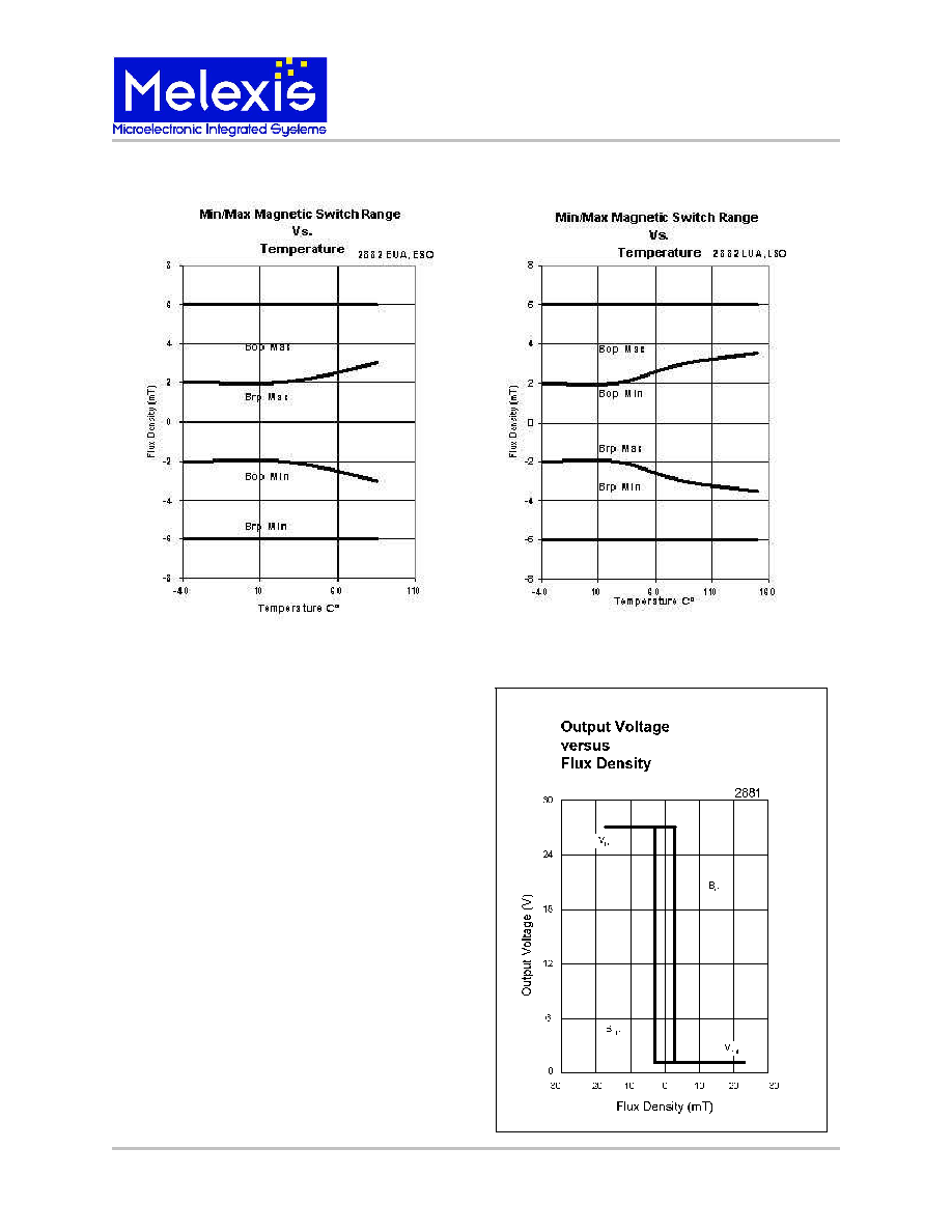
US2881 Magnetic Specifications
Parameter
Symbol
Test Conditions
Min
Typ
Max
Units
Operating Point
B
OP
E/L UA, E/L SO, Ta= 25
Vdd=3.5 & 24 volts DC Vdd
0.5
2.0
4.5
mT
Release Point
B
RP
E/L UA, E/L SO, Ta= 25
Vdd=3.5 & 24 volts DC Vdd
-4.5
-2.0
-0.5
mT
Hysteresis
B
hys
E/L UA, E/L SO, Ta= 25
Vdd=3.5 & 24 volts DC Vdd
1.5
4.0
5.0
mT
Operating Point
B
OP
EUA, ESO, Ta= 85
Vdd=3.5 & 24 volts DC Vdd
-1.0
2.0
6.0
mT
Release Point
B
RP
EUA, ESO, Ta= 85
Vdd=3.5 & 24 volts DC Vdd
-6.0
-2.0
-1.0
mT
Hysteresis
B
hys
EUA, ESO, Ta= 85
Vdd=3.5 & 24 volts DC Vdd
1.5
4.0
5.5
mT
Operating Point
B
OP
LUA, LSO, Ta=150∞C,
Vdd=3.5 & 24 volts DC Vdd
-2.0
2.0
6.0
mT
Release Point
B
RP
LUA, LSO, Ta=150∞C,
Vdd=3.5 & 24 volts DC Vdd
-6.0
-2.0
2.0
mT
Hysteresis
B
hys
LUA, LSO, Ta=150∞C,
Vdd=3.5 & 24 volts DC Vdd
1.5
4.0
5.5
mT
Note: 1 mT = 10 Gauss.

3901002881
Page 3
Aug/02
Rev. 008
Absolute Maximum Ratings
Supply Voltage (Operating), V
DD
24V
Supply Current (Fault), I
DD
50mA
Output Voltage, V
OUT
24V
Output Current (Fault), I
OUT
50mA
Power Dissipation, P
D
100mW
Operating Temperature Range, T
A
-40 to 150∞C
Storage Temperature Range, T
S
-65 to 150∞C
Maximum Junction Temp, T
J
175∞C
US2882 Magnetic Specifications
Parameter
Symbol Test Conditions
Min
Typ
Max
Units
Operating Point
B
OP
E/L UA, E/L SO, Ta= 25
Vdd=3.5 & 24 volts DC Vdd
-2.0
2.0
6.0
mT
Release Point
B
RP
E/L UA, E/L SO, Ta= 25
Vdd=3.5 & 24 volts DC Vdd
-6.0
-2.0
2.0
mT
Hysteresis
B
hys
E/L UA, E/L SO, Ta= 25
Vdd=3.5 & 24 volts DC Vdd
1.5
4.0
5.0
mT
Operating Point
B
OP
EUA, ESO, Ta= 85
Vdd=3.5 & 24 volts DC Vdd
-3.0
2.0
6.0
mT
Release Point
B
RP
EUA, ESO, Ta= 85
Vdd=3.5 & 24 volts DC Vdd
-6.0
-2.0
3.0
mT
Hysteresis
B
hys
EUA, ESO, Ta= 85
Vdd=3.5 & 24 volts DC Vdd
1.5
4.0
6.0
mT
Operating Point
B
OP
LUA, LSO, Ta=150∞C,
Vdd=3.5 & 24 volts DC Vdd
-3.5
2.0
6.0
mT
Release Point
B
RP
LUA, LSO, Ta=150∞C,
Vdd=3.5 & 24 volts DC Vdd
-6.0
-2.0
3.5
mT
Hysteresis
B
hys
LUA, LSO, Ta=150∞C,
Vdd=3.5 & 24 volts DC Vdd
1.5
4.0
6.0
mT

3901002881
Page 4
Aug/02
Rev. 008
Performance Graphs
3901002881
Page 5
Aug/02
Rev. 008