 | –≠–ª–µ–∫—Ç—Ä–æ–Ω–Ω—ã–π –∫–æ–º–ø–æ–Ω–µ–Ω—Ç: MXR2999ML | –°–∫–∞—á–∞—Ç—å:  PDF PDF  ZIP ZIP |

MEMSIC MXR2999GL/ML
Page 1 of 6
2002.08.30.1
Improved
±1 g Dual Axis
Accelerometer with Ratiometric
Outputs
MXR2999GL/ML
FEATURES
Resolution better than 1 milli-g
Dual axis accelerometer fabricated on a monolithic CMOS IC
On chip mixed mode signal processing
No moving parts
50,000 g shock survival rating
17 Hz bandwidth expandable to >160 Hz
3.0V to 5.25V single supply continuous operation
Continuous self test
Independent axis programmability (special order)
Compensated for Sensitivity over temperature
Ultra low initial Zero-g Offset
APPLICATIONS
Automotive ≠ Vehicle Security/Vehicle Stability control/
Headlight Angle Control/Tilt Sensing
Security ≠ Gas Line/Elevator/Fatigue Sensing/Computer Security
Information Appliances ≠ Computer Peripherals/PDA's/Mouse
Smart Pens/Cell Phones
Internal
Oscillator
Sck
(optional)
CLK
Heater
Control
X axis
Y axis
Factory Adjust
Offset & Gain
Low Pass
Filter
Low Pass
Filter
Temperature
Sensor
Voltage
Reference
V
REF
A
OUTX
V
DD
V
DA
Gnd
2-AXIS
SENSOR
A
OUTY
T
OUT
Continous
Self Test
MXR2999GL/ML FUNCTIONAL BLOCK DIAGRAM
Gaming ≠ Joystick/RF Interface/Menu Selection/Tilt Sensing
GPS ≠ Electronic compass tilt correction
Consumer ≠ LCD projectors, pedometers, blood pressure
Monitor, digital cameras
GENERAL DESCRIPTION
The MXR2999GL/ML is a low cost, dual axis
accelerometer fabricated on a standard, submicron CMOS
process. It is a complete sensing system with on-chip
mixed mode signal processing. The MXR2999GL/ML
measures acceleration with a full-scale range of
±1 g and a
sensitivity of 1000mV/g. (The MEMSIC accelerometer
product line extends from
±.5 g to ±200 g with custom
versions available above
±10 g.) It can measure both
dynamic acceleration (e.g. vibration) and static acceleration
(e.g. gravity). The MXR2999GL/ML design is based on
heat convection and requires no solid proof mass. This
eliminates stiction and particle problems associated with
competitive devices and provides shock survival of 50,000
g, leading to significantly lower failure rate and lower loss
due to handling during assembly.
The MXR2999GL/ML provides a ratiometric analog output
that is proportional to 50% of the supply voltage at zero g
acceleration. The typical noise floor is 0.2 mg/ Hz
allowing signals below 1 milli-g to be resolved at 1 Hz
bandwidth. The 3dB rolloff of the device occurs at 17 Hz
but is expandable to >160 Hz (reference Application Note
AN-00MX-003). The MXR2999GL/ML is packaged in a
hermetically sealed LCC surface mount package (5 mm x 5
mm x 2 mm height) and is operational over a -40
∞C
to
105
∞C(ML) and 0∞C to 70∞C(GL) temperature range.
Information furnished by MEMSIC is believed to be accurate and reliable.
However, no responsibility is assumed by MEMSIC for its use, nor for any
infringements of patents or other rights of third parties which may result from
its use. No license is granted by implication or otherwise under any patent or
patent rights of MEMSIC.
MEMSIC, Inc.
800 Turnpike St., Suite 202, North Andover, MA 01845
Tel: 978.738.0900
Fax: 978.738.0196
www.memsic.com

MEMSIC MXR2999GL/ML
Page 2 of 6
2002.08.30.1
MXR2999GL/ML SPECIFICATIONS
(Measurements @ 25
∞C, Acceleration = 0 g unless otherwise noted; V
DD
, V
DA
= 5.0V unless
otherwise specified)
Parameter
Conditions
Min
MXR2999GL
Typ
Max
Min
MXR2999ML
Typ
Max
Units
SENSOR INPUT
Measurement Range
1
Each Axis
±1.0
±1.0
g
Nonlinearity
Best fit straight line
0.5
0.5
% of FS
Alignment Error
2
X Sensor to Y Sensor
±1.0
±1.0
degrees
Transverse Sensitivity
3
±2.0
±2.0
%
SENSITIVITY
Sensitivity, Analog Outputs at
pins
A
OUTX
and A
OUTY
5
Each Axis
950
1000
1050
950
1000
1050
mV/g
Change over Temperature
-10
+8
-25
+8
%
ZERO g BIAS LEVEL
0 g Offset
5
Each Axis
-0.1
0.0
+0.1
-0.1
0.0
+0.1
g
0 g Voltage
5
2.4
2.50
2.6
2.4
2.50
2.6
V
0 g Offset over Temperature
Based on 1000 mV/g
±1.5
±1.5
±1.5
±1.5
mg/
∞C
mV/
∞C
NOISE PERFORMANCE
Noise Density, rms
Without frequency
compensation
0.2
0.4
0.2
0.4
mg/
Hz
FREQUENCY RESPONSE
3dB Bandwidth - uncompensated
12
17
12
17
Hz
3dB Bandwidth ≠ compensated
4
>160
>160
Hz
TEMPERATURE OUTPUT
T
out
Voltage
1.21
1.25
1.29
1.21
1.25
1.29
V
Sensitivity
4.6
5.0
5.4
4.6
5.0
5.4
mV/
∞K
VOLTAGE REFERENCE
V
Ref
@3.0V-5.0V
supply
2.4
2.5 2.65
2.4 2.5 2.65
V
Change over Temperature
0.1
0.1
mV/
∞C
Current Drive Capability
Source
100
100
µA
SELF TEST
Continuous Voltage at A
OUTX
,
A
OUTY
under Failure
@5.0V Supply, output
rails to
supply voltage
5.0
5.0
V
Continuous Voltage at A
OUTX
,
A
OUTY
under Failure
@3.0V Supply, output
rails to
supply voltage
3.0
3.0
V
A
OUTX
and A
OUTY
OUTPUTS
Normal Output Range
@5.0V Supply
@3.0V Supply
0.1
0.1
4.9
2.9
0.1
0.1
4.9
2.9
V
V
Current
Source or sink, @
3.0V-5.0V supply
100
100
µA
Turn-On Time
@5.0V Supply
@3.0V Supply
100
40
100
40
mS
mS
POWER SUPPLY
Operating Voltage Range
3.0
5.25
3.0
5.25
V
Supply Current
@ 5.0V
2.7 3.8 4.4
2.7 3.8
4.4
mA
Supply Current
5
@
3.0V
3.2
4.7
5.4 3.2
4.7 5.4 mA
TEMPERATURE RANGE
Operating Range
0
+70
-40
+105
∞C
NOTES
1
Guaranteed by measurement of initial offset and sensitivity.
2
Alignment error is specified as the angle between the true and indicated axis of
sensitivity.
3
Transverse sensitivity is the algebraic sum of the alignment and the inherent
sensitivity errors.
4
External circuitry is required to extend the 3dB bandwidth (ref. Application Note:
AN-00MX-003)
5
The device operates over a 3.0V to 5.25V supply range. Please note that sensitivity
and zero g bias level will be slightly different at 3.0V operation. For devices to be
operated at 3.0V in production, they can be trimmed at the factory specifically for
this lower supply voltage operation, in which case the sensitivity and zero g bias
level specifications on this page will be met. Please contact the factory for specially
trimmed devices for low supply voltage operation.

MEMSIC MXR2999GL/ML
Page 3 of 6
2002.08.30.1
ABSOLUTE MAXIMUM RATINGS*
Supply Voltage (V
DD
, V
DA
) .....................-0.5 to +7.0V
Storage Temperature ......................-65
∞C to +150∞C
Acceleration ............................................50,000 g
*Stresses above those listed under Absolute Maximum Ratings may cause permanent
damage to the device. This is a stress rating only; the functional operation of the
device at these or any other conditions above those indicated in the operational
sections of this specification is not implied. Exposure to absolute maximum rating
conditions for extended periods may affect device reliability.
Package Characteristics
Package
JA
JC
Device Weight
LCC-8
110
∞C/W 22∞C/W
< 1 gram
Pin Description: LCC-8 Package
Pin Name Description
1 T
OUT
Temperature (Analog Voltage)
2 A
OUTY
Y-Axis Acceleration Signal
3 Gnd Ground
4 V
DA
Analog Supply Voltage
5 A
OUTX
X-Axis Acceleration Signal
6 V
ref
2.5V
Reference
7
Sck
Optional External Clock
8 V
DD
Digital Supply Voltage
Ordering Guide
Model
Package Style
Temperature Range
MXR2999GL
LCC - 8
0 to 70
∞C
MXR2999ML
LCC - 8
-40 to 105
∞C
All parts are shipped in tape and reel packaging.
Caution:
ESD (electrostatic discharge) sensitive device.
8
4
1
2
3
7
6
5
Top View
ME
MS
I
C
X +g
Y +g
Note: The MEMSIC logo's arrow indicates the +X sensing
direction of the device. The +Y sensing direction is rotated 90∞
away from the +X direction following the right-hand rule.
THEORY OF OPERATION
The MEMSIC device is a complete dual-axis acceleration
measurement system fabricated on a monolithic CMOS IC
process. The device operation is based on heat transfer by
natural convection and operates like other accelerometers
having a proof mass. The stationary element, or `proof
mass', in the MEMSIC sensor is a gas.
A single heat source, centered in the silicon chip is
suspended across a cavity. Equally spaced
aluminum/polysilicon thermopiles (groups of
thermocouples) are located equidistantly on all four sides of
the heat source (dual axis). Under zero acceleration, a
temperature gradient is symmetrical about the heat source,
so that the temperature is the same at all four thermopiles,
causing them to output the same voltage.
Acceleration in any direction will disturb the temperature
profile, due to free convection heat transfer, causing it to be
asymmetrical. The temperature, and hence voltage output
of the four thermopiles will then be different. The
differential voltage at the thermopile outputs is directly
proportional to the acceleration. There are two identical
acceleration signal paths on the accelerometer, one to
measure acceleration in the x-axis and one to measure
acceleration in the y-axis. Please visit the MEMSIC
website at www.memsic.com for a picture/graphic
description of the free convection heat transfer principle.
MEMSIC MXR2999GL/ML
Page 4 of 6
2002.08.30.1
MXR2999GL/ML PIN DESCRIPTIONS
V
DD
≠ This is the supply input for the digital circuits and
the sensor heater in the accelerometer. The DC voltage
should be between 3.0 and 5.25 volts. Refer to the section
on PCB layout and fabrication suggestions for guidance on
external parts and connections recommended.
V
DA
≠ This is the power supply input for the analog
amplifiers in the accelerometer. Refer to the section on
PCB layout and fabrication suggestions for guidance on
external parts and connections recommended.
Gnd ≠ This is the ground pin for the accelerometer.
A
OUTX
≠ This pin is the output of the x-axis acceleration
sensor. The user should ensure the load impedance is
sufficiently high as to not source/sink >100
µA. While the
sensitivity of this axis has been programmed at the factory
to be the same as the sensitivity for the y-axis, the
accelerometer can be programmed for non-equal
sensitivities on the x- and y-axes. Contact the factory for
additional information on this feature.
A
OUTY
≠
This pin is the output of the y-axis acceleration
sensor. The user should ensure the load impedance is
sufficiently high as to not source/sink >100
µA. While the
sensitivity of this axis has been programmed at the factory
to be the same as the sensitivity for the x-axis, the
accelerometer can be programmed for non-equal
sensitivities on the x- and y-axes. Contact the factory for
additional information on this feature.
T
OUT
≠ This pin is the buffered output of the temperature
sensor. The analog voltage at T
OUT
is an indication of the
die temperature. This voltage is useful as a differential
measurement of temperature from ambient and not as an
absolute measurement of temperature
Sck ≠ The standard product is delivered with an internal
clock option (800kHz). This pin should be grounded
when operating with the internal clock. An external
clock option can be special ordered from the factory
allowing the user to input a clock signal between 400kHz
and 1.6MHz.
V
ref
≠ A reference voltage is available from this pin. It is
set at 2.50V typical and has 100
µA of drive capability.
DISCUSSION OF TILT APPLICATIONS AND
RESOLUTION
Tilt Applications: One of the most popular applications of
the MEMSIC accelerometer product line is in
tilt/inclination measurement. An accelerometer uses the
force of gravity as an input to determine the inclination
angle of an object.
A MEMSIC accelerometer is most sensitive to changes in
position, or tilt, when the accelerometer's sensitive axis is
perpendicular to the force of gravity, or parallel to the
Earth's surface. Similarly, when the accelerometer's axis is
parallel to the force of gravity (perpendicular to the Earth's
surface), it is least sensitive to changes in tilt.
Table 1 and Figure 2 help illustrate the output changes in
the X- and Y-axes as the unit is tilted from +90
∞ to 0∞.
Notice that when one axis has a small change in output per
degree of tilt (in mg), the second axis has a large change in
output per degree of tilt. The complementary nature of
these two signals permits low cost accurate tilt sensing to
be achieved with the MEMSIC device (reference
application note AN-00MX-007).
Top View
X
Y
+90
0
0
0
gravity
ME
M
S
I
C
Figure 2: Accelerometer Position Relative to Gravity
X-Axis
Y-Axis
X-Axis
Orientatio
n
To Earth's
Surface
(deg.)
X Output
(g)
Change
per deg.
of tilt
(mg)
Y Output
(g)
Change
per deg.
of tilt
(mg)
90
1.000
0.15 0.000
17.45
85
0.996
1.37 0.087
17.37
80
0.985
2.88 0.174
17.16
70
0.940
5.86 0.342
16.35
60
0.866
8.59 0.500
15.04
45
0.707
12.23 0.707
12.23
30
0.500
15.04 0.866
8.59
20
0.342
16.35 0.940
5.86
10
0.174
17.16 0.985
2.88
5
0.087
17.37 0.996
1.37
0
0.000
17.45 1.000
0.15
Table 1: Changes in Tilt for X- and Y-Axes
Resolution: The accelerometer resolution is limited by
noise. The output noise will vary with the measurement
bandwidth. With the reduction of the bandwidth, by
applying an external low pass filter, the output noise drops.
Reduction of bandwidth will improve the signal to noise
ratio and the resolution. The output noise scales directly
with the square root of the measurement bandwidth. The
maximum amplitude of the noise, its peak- to- peak value,
approximately defines the worst case resolution of the
measurement. With a simple RC low pass filter, the rms
noise is calculated as follows:
MEMSIC MXR2999GL/ML
Page 5 of 6
2002.08.30.1
Noise (mg rms) = Noise(mg/ Hz ) *
)
6
.
1
*
)
(
(
Hz
Bandwidth
The peak-to-peak noise is approximately equal to 6.6 times
the rms value (for an average uncertainty of 0.1%).
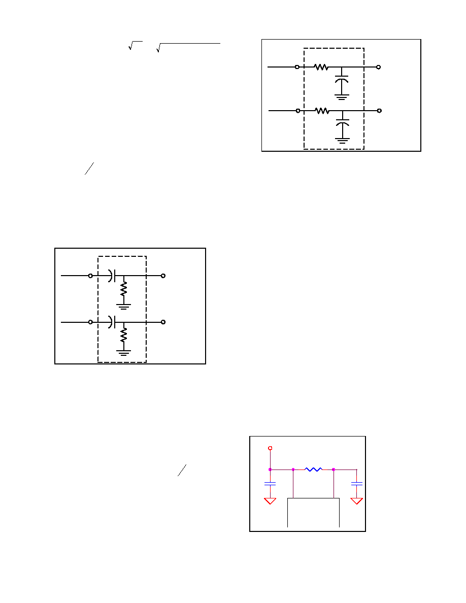
EXTERNAL FILTERS
AC Coupling: For applications where only dynamic
accelerations (vibration) are to be measured, it is
recommended to ac couple the accelerometer output as
shown in Figure 3. The advantage of ac coupling is that
variations from part to part of zero g offset and zero g
offset versus temperature can be eliminated. Figure 3 is a
HPF (high pass filter) with a ≠3dB breakpoint given by the
equation:
RC
f
2
1
=
. In many applications it may be
desirable to have the HPF ≠3dB point at a very low
frequency in order to detect very low frequency
accelerations. Sometimes the implementation of this HPF
may result in unreasonably large capacitors, and the
designer must turn to digital implementations of HPFs
where very low frequency ≠3dB breakpoints can be
achieved.
A
OUTX
R
C
A
OUTY
R
C
A
OUTX
Filtered
Output
A
OUTY
Filtered
Output
Figure 3: High Pass Filter
Low Pass Filter: An external low pass filter is useful in
low frequency applications such as tilt or inclination. The
low pass filter limits the noise floor and improves the
resolution of the accelerometer. When designing with
MEMSIC ratiometric output accelerometers (MXRxxxx
series), it is highly recommended that an external, 20 Hz
low pass filter be used to eliminate internally generated
periodic noise that is coupled to the output of the
accelerometer. The low pass filter shown in Figure 4 has a
≠3dB breakpoint given by the equation:
RC
f
2
1
=
. For
the 200 Hz ratiometric output device filter, C=0.2
µF and
R=39k
, ±5%, 1/8W.
A
OUTX
R
C
A
OUTY
R
C
A
OUTX
Filtered
Output
A
OUTY
Filtered
Output
Figure 4: Low Pass Filter
USING THE ACCELEROMETER IN VERY LOW
POWER APPLICATIONS (BATTERY OPERATION)
In applications with power limitations, power cycling can
be used to extend the battery operating life. One important
consideration when power cycling is that the accelerometer
turn on time limits the frequency bandwidth of the
accelerations to be measured. For example, operating at
3.0V the turn on time is 40mS. To double the operating
time, a particular application may cycle power ON for
40mS, then OFF for 40mS, resulting in a measurement
period of 80mS, or a frequency of 12.5Hz. With a
frequency of measurements of 12.5Hz, accelerations
changes as high as 6.25Hz can be detected. Power cycling
can be used effectively in many inclinometry applications,
where inclination changes can be slow and infrequent.
POWER SUPPLY NOISE REJECTION
Two capacitors and a resistor are recommended for best
rejection of power supply noise (reference Figure 5 below).
The capacitors should be located as close as possible to the
device supply pins (V
DA
, V
DD
). The capacitor lead length
should be as short as possible, and surface mount capacitors
are preferred. For typical applications, capacitors C1 and
C2 can be ceramic 0.1 µF, and the resistor R can be 10 .
In 5V applications where power consumption is not a
concern, maximum supply noise rejection can be obtained
by significantly increasing the values of C1, C2 and R. For
example, C1 = C2 = 0.47 µF and R = 270 will virtually
eliminate power supply noise effects.
R
MEMSIC
Accelerometer
VDA
C1
C2
VDD
V SUPPLY
Figure 5: Power Supply Noise Rejection