 | –≠–ª–µ–∫—Ç—Ä–æ–Ω–Ω—ã–π –∫–æ–º–ø–æ–Ω–µ–Ω—Ç: MCRF044 | –°–∫–∞—á–∞—Ç—å:  PDF PDF  ZIP ZIP |
February 9, 2000
1
MICRF004/RF044
MICRF004/RF044
Micrel
MICRF004
QwikRadioTM Low-Power VHF Receiver
Final Information
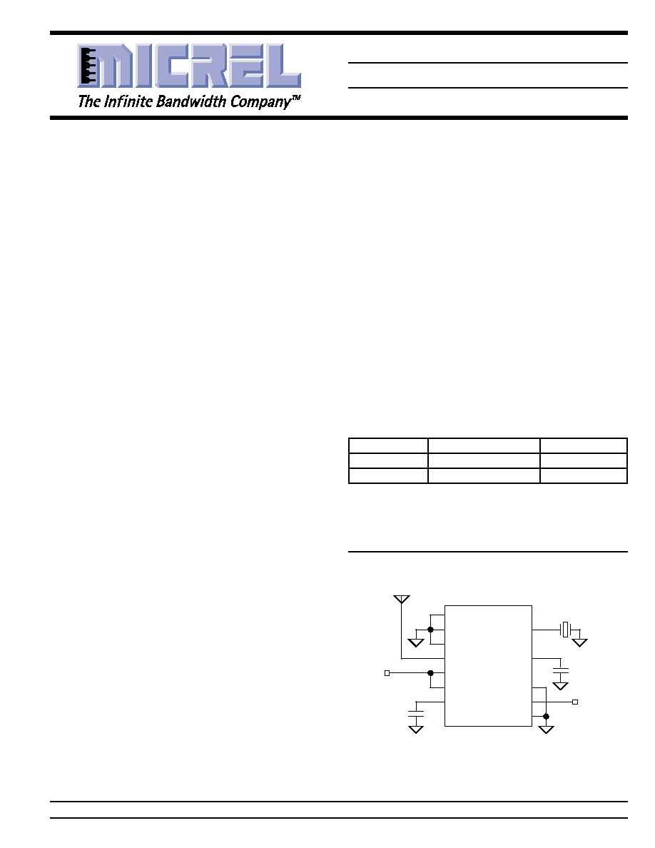
Typical Application
SEL0
SEL0
SWEN
VSSRF
REFOSC
VSSRF
SEL1
ANT
CAGC
VDDRF
WAKEB
VDDBB
SHUT
CTH
DO
NC
VSSBB
0.047µF
4.85MHz
(ceramic resonator)
Data
Output
MICRF004
4.7µF
+5V
150MHz 1200b/s On-Off Keyed Receiver
Features
∑ Complete VHF receiver on a monolithic chip
∑ 140MHz to 200MHz frequency range
∑ >200 meters typical range with monopole antenna
∑ 2.5kb/s sweep- and 10kb/s fixed-mode data rates
∑ Automatic tuning, no manual adjustment
∑ No filters or inductors required
∑ Low 240
µ
A operating supply current at 150MHz
(10:1 duty cycle)
∑ Shutdown mode for >100:1 duty-cycle operation
∑ Wakeup for enabling decoders and microprocessors
∑ Very low RF antenna reradiation
∑ CMOS logic interface for standard ICs
∑ Extremely low external part count
Applications
∑ Automotive remote keyless entry
∑ Long range RF identification
∑ Remote fan and light control
∑ Garage door and gate openers
Ordering Information
Part Number
Junction Temp. Range
Package
MICRF004BM
≠40
∞
C to +85
∞
C
16-Lead SOP
MICRF004BN
≠40
∞
C to +85
∞
C
16-Pin DIP
8-pin versions available. See "Custom 8-Pin Options," following page.
Micrel, Inc. ∑ 1849 Fortune Drive ∑ San Jose, CA 95131 ∑ USA ∑ tel + 1 (408) 944-0800 ∑ fax + 1 (408) 944-0970 ∑ http://www.micrel.com
QwikRadio is a trademark of Micrel, Inc. The QwikRadio ICs were developed under a partnership agreement with AIT of Orlando, Florida.
General Description
The MICRF004 QwikRadioTM VHF receiver is a single-chip
OOK (on-off keyed) receiver IC for remote wireless applica-
tions. This device is a true single-chip, "antenna-in, data-out"
device. All RF and IF tuning is accomplished automatically
within the IC which eliminates manual tuning production
costs and results in a highly reliable, extremely low-cost
solution for high-volume wireless applications.
The MICRF004 is extremely easy to apply, minimizing design
and production costs, and improving time to market. The
MICRF004 provides two fundamental modes of operation,
fixed and sweep.
In fixed mode, the device functions as a conventional super-
heterodyne receiver with an internal local oscillator operating
at a single frequency based on an external reference crystal
or clock. Fixed mode is for use with accurately-controlled
transmitters utilizing crystal or SAW (surface acoustic wave)
resonators.
In sweep mode, the MICRF004 sweeps the internal local
oscillator at rates greater than the baseband data rate. This
effectively broadens the RF bandwidth of the receiver to a
value equivalent to conventional superregenerative receiv-
ers. This allows the MICRF004 to operate with less expensive
LC transmitters without additional components or tuning,
even though the receiver topology is still superheterodyne. In
this mode the reference crystal can be replaced with a less
expensive
±
0.5% ceramic resonator.
The MICRF004 features a shutdown control, which may be
used for duty-cycled operation, and a wake-up output, which
provides a logical indication of an incoming RF signal. These
features make the MICRF004 ideal for low- and ultra-low-
power applications, such as RKE (remote keyless entry) and
RFID (RF identification).
Since all post-detection (demodulator) data filtering is pro-
vided on the MICRF004, no external filters are required. One
of the four internal filter bandwidths must be externally
selected based on data rate and code modulation format.
Bandwidths range in binary steps, from 0.55kHz to 4.4kHz
(sweep mode) or 1.1kHz to 8.8kHz (fixed mode).
MICRF004/RF044
Micrel
MICRF004
2
February 9, 2000
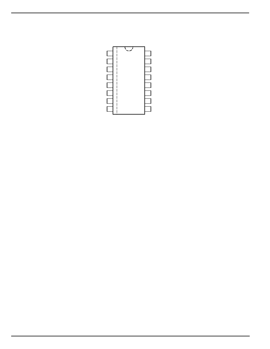
Pin Configuration
1
SEL0
VSSRF
VSSRF
ANT
VDDRF
VDDBB
CTH
NC
16 SWEN
REFOSC
SEL1
CAGC
WAKEB
SHUT
DO
VSSBB
15
14
13
12
11
10
9
2
3
4
5
6
7
8
16-Pin DIP (N) or SOP (M) Packages

February 9, 2000
3
MICRF004/RF044
MICRF004/RF044
Micrel
Pin Description
Pin Number
Pin Number
Pin Name
Pin Function
16-Pin Pkg.
8-Pin Pkg.
1
SEL0
Bandwidth Selection Bit 0 (Input): Configure with SEL1 to set the desired
demodulator filter bandwidth. See Table 1. Internally pulled-up to VDDRF.
2, 3
1
VSSRF
RF [Analog] Return (Input): Ground return to the RF section power supply.
See "Application Information" for bypass capacitor details.
4
2
ANT
Antenna (Input): High-impedance, internally ac coupled receiver input.
Connect this pin to the receive antenna. This FET gate input has approxi-
mately 2pF of shunt (parasitic) capacitance. See "Applications Information"
for optional band-pass filter information.
5
3
VDDRF
RF [Analog] Supply (Input): Positive supply input for the RF section of the
IC. VDDBB and VDDRF should be connected together directly at the IC
pins. Connect a low ESL, low ESR decoupling capacitor from this pin to
VSSRF, as short as possible.
6
VDDBB
Base-Band [Digital] Supply (Input): Positive supply input for the baseband
section of the IC. VDDBB and VDDRF should be connected together at the
IC pins.
7
4
CTH
[Data Slicing] Threshold Capacitor (External Component): Capacitor
extracts the dc average value from the demodulated waveform which
becomes the reference for the internal data slicing comparator. See "Appli-
cations Information" for selection.
8
NC
not internally connected
9
VSSBB
Base-Band [Digital] Return (Input): Ground return to the baseband section
power supply. See "Application Information" for bypass capacitor and layout
details.
10
5
DO
Digital Output (Output): CMOS-level compatible data output signal.
11
6
SHUT
Shutdown (Input): Shutdown-mode logic-level control input. Pull low to
enable the receiver. This input has an internal pulled-up to VDDRF.
12
WAKEB
Wakeup (Output): Active-low output that indicates detection of an incoming
RF signal. Signal is determined by monitoring for data preamble. CMOS-
level compatible.
13
7
CAGC
AGC Capacitor (External Component): Integrating capacitor for on-chip
AGC (automatic gain control). The decay/attack time-constant (
) ratio is
nominally 10:1. See "Applications Information" for capacitor selection.
14
SEL1
Bandwidth Selection Bit 1 (Input): Configure with SEL0, programs to set the
desired demodulator filter bandwidth. See Table 1. Internally pulled-up to
VDDRF.
15
8
REFOSC
Reference Oscillator (External Component or Input): Timing reference for
on-chip tuning and alignment. Connect either a ceramic resonator or crystal
(mode dependent, see "Application Information"). between this pin and
VSSBB, or drive the input with an ac-coupled 0.5Vpp input clock.
16
SWEN
Sweep-Mode Enable (Input): Sweep- or fixed-mode operation control input.
When VSWEN is high, the MICRF004 is in sweep mode; when SWEN is
low, the receiver operates as a conventional single-conversion superhetero-
dyne receiver. This pin is internally pulled-up to VDDRF.

MICRF004/RF044
Micrel
MICRF004
4
February 9, 2000
Electrical Characteristics
V
DDRF
= V
DDBB
= V
DD
where +4.75V
V
DD
5.5V, V
SS
= 0V; C
AGC
= 4.7
µ
F, C
TH
= 0.047
µ
F; f
REFOSC
= 4.65MHz; T
A
= 25
∞
C, bold
values indicate ≠40
∞
C
T
A
+85
∞
C; current flow into device pins is positive; unless noted.
Symbol
Parameter
Condition
Min
Typ
Max
Units
I
OP
Operating Current
continuous operation
2.4
mA
10:1 duty cycle
240
µ
A
I
STBY
Standby Current
V
SHUT
= V
DD
0.35
µ
A
RF Section, IF Section
Receiver Sensitivity
Notes 4, 6
≠80
dBm
f
IF
IF Center Frequency
Note 7
0.86
MHz
f
BW
IF 3dB Bandwidth
Notes 6, 7
0.43
MHz
f
ANT
RF Input Range
145
200
MHz
Z
IN(ant)
Antenna Input Impdeance
f
IN
= 150MHz
422
Receive Modulation Duty-Cycle
20
80
%
Maximum Receiver Input
R
SC
= 50
≠20
dBm
Spurious Reverse Isolation
ANT pin, R
SC
= 50
, Note 5
30
µ
Vrms
AGC Attack to Decay Ratio
t
ATTACK
˜
t
DECAY
0.1
AGC Leakage Current
T
A
= +85
∞
C
±
200
nA
Reference Oscillator
Reference Oscillator
extermal reference (250mV peak)
6
ms
Stabilization Time
ceramic resonator
5
ms
crystal
10
ms
Z
REFOSC
Reference Oscillator
290
k
Input Impedance
Reference Oscillator
Note 10
0.1
2
Vp-p
Input Sensitivity
I
REFOSC
Reference Oscillator Current
4.5
µ
A
Demodulator
Z
CTH
CTH Source Impedance
Note 8
124
k
Z
CTH
CTH Source Impedance Variation
±
15
%
I
ZCTH(leak)
CTH Leakage Current
T
A
= +85
∞
C
±
200
nA
Demodulator Filter Bandwidth
V
SEL0
= V
SEL1
= V
SWEN
= V
DD
, Notes 7, 9
3960
Hz
Demodulator Filter Bandwidth
V
SEL0
= V
SEL1
= V
DD
, V
SWEN
= V
SS
,
7930
Hz
Note 7, 9
Absolute Maximum Ratings
(Note 1)
Supply Voltage (V
DDRF
, V
DDBB
) .................................... +7V
Reference Oscillator Input Voltage (V
REFOSC
) .......... V
DDBB
Input/Output Voltage (V
I/O
) ................. V
SS
≠0.3 to V
DD
+0.3
Junction Temperature (T
J
) ...................................... +150
∞
C
Storage Temperature Range (T
S
) ............ ≠65
∞
C to +150
∞
C
Lead Temperature (soldering, 10 sec.) ................... +260
∞
C
ESD Rating, Note 3
Operating Ratings
(Note 2)
Supply Voltage (V
DDRF
, V
DDBB
) ................ +4.75V to +5.5V
Ambient Temperature (T
A
) ......................... ≠40
∞
C to +85
∞
C
Package Thermal Resistance (
JA
)
16-pin DIP (
JA
) ................................................... 90
∞
C/W
16-pin SOIC (
JA
) .............................................. 120
∞
C/W

February 9, 2000
5
MICRF004/RF044
MICRF004/RF044
Micrel
Symbol
Parameter
Condition
Min
Typ
Max
Units
Digital/Control Section
I
IN(pu)
Input Pull up Current
SEL0, SEL1, SWEN, V
SHUT
= V
SS
8
µ
A
V
IN(high)
Input High Voltage
SEL0, SEL1, SWEN
0.8V
DD
V
V
IN(low)
Input Low Voltage
SEL0, SEL1, SWEN
0.2V
DD
V
I
OUT
Output Current
DO, WAKEB pins, push-pull
10
µ
A
V
OUT(high)
Output High Voltage
DO, WAKEB pins, I
OUT
= ≠1
µ
A
0.9V
DD
V
V
OUT(low)
Output Low Voltage
DO, WAKEB pins, I
OUT
= +1
µ
A
0.1V
DD
V
t
R
, t
F
Output Rise and Fall Times
DO, WAKEB pins, C
LOAD
= 15pF
10
µ
s
t
WAKEB
Wakeup Output Time
RF
IN
= TBDdBm,
4
ms
V
SEL0
= V
SEL1
= V
SWEN
= V
SHUT
= V
SS
Note 1.
Exceeding the absolute maximum rating may damage the device.
Note 2.
The device is not guaranteed to function outside its operating rating.
Note 3.
Devices are ESD sensitive. Use appropriate ESD precautions. Meets class 1 ESD test requirements, (human body model HBM), in accor-
dance with MIL-STD-883C, method 3015. Do not operate or store near strong electrostatic fields.
Note 4:
Sensitivity is defined as the average signal level measured at the input necessary to achieve 10
-2
BER (bit error rate). The input signal is
defined as a return-to-zero (RZ) waveform with 50% average duty cycle (Manchester encoded data) at a data rate of 300b/s. The RF input is
assumed to be matched into 50
.
Note 5:
Spurious reverse isolation represents the spurious components which appear on the RF input pin (ANT) measured into 50
with an input RF
matching network.
Note 6:
Sensitivity, a commonly specified receiver parameter, provides an indication of the receiver's input referred noise, generally input thermal
noise. However, it is possible for a more sensitive receiver to exhibit range performance no better than that of a less sensitive receiver if the
background noise is appreciably higher than the thermal noise. Background noise refers to other interfering signals, such as FM radio
stations, pagers, etc.
A better indicator of achievable receiver range performance is usually given by its selectivity, often stated as fntermediate frequency (IF) or
radio frequency (RF) bandwidth, depending on receiver topology. Selectivity is a measure of the rejection by the receiver of "ether" noise.
More selective receivers will almost invariably provide better range. Only when the receiver selectivity is so high that most of the noise on the
receiver input is actually thermal will the receiver demonstrate sensitivity-limited performance.
Note 7:
Parameter scales linearly with reference oscillator frequency f
T
. For any reference oscillator frequency other than 4.65MHz, compute new
parameter value as the ratio:
f
MHz
4.65
(parameter value at 4.65MHz)
REFOSC
◊
Example: For reference oscillator freqency f
T
= 6.00MHz:
(parameter value at 6.00MHz)
6.00
4.65
(paramter value at 4.65MHz)
=
◊
Note 8:
Parameter scales inversely with reference oscillator frequency f
T
. For any reference oscillator frequency other than 4.65MHz, compute new
parameter value as the ratio:
4.65
f
MHz
(parmeter value at 4.65MHz)
REFOSC
◊
Example: For reference oscillator frequency f
T
= 6.00MHz:
(parmeter value at 4.65MHz)
4.65
6.00
(parmeter value at 4.65MHz)
=
◊
Note 9:
Demodulator filter bandwidths are related in a binary manner, so any of the (lower) nominal filter values may be derived simply by dividing this
parameter value by 2, 4, or 8 as desired.
Note 10: External signal generator used. When a crystal or ceramic resonator is used, the minimum voltage is 300mVp-p. The reference oscillator
voltage amplitude is a function of the quality of the ceramic or crystal resonator.