 | –≠–ª–µ–∫—Ç—Ä–æ–Ω–Ω—ã–π –∫–æ–º–ø–æ–Ω–µ–Ω—Ç: MIC2025 | –°–∫–∞—á–∞—Ç—å:  PDF PDF  ZIP ZIP |

March 2000
1
MIC2025/2075
MIC2025/2075
Micrel
MIC2025/2075
Single-Channel Power Distribution Switch
Preliminary Information
General Description
The MIC2025 and MIC2075 are high-side MOSFET switches
optimized for general-purpose power distribution requiring
circuit protection.
The MIC2025/75 are internally current limited and have
thermal shutdown that protects the device and load. The
MIC2075 offers "smart" thermal shutdown that reduces cur-
rent consumption in fault modes. When a thermal shutdown
fault occurs, the output is latched off until the faulty load is
removed. Removing the load or toggling the enable input will
reset the device output.
Both devices employ soft-start circuitry that minimizes inrush
current in applications where highly capacitive loads are
employed. A fault status output flag is provided that is
asserted during overcurrent and thermal shutdown condi-
tions.
The MIC2025/75 is available in the MM8TM 8-lead MSOP and
8-lead SOP.
Typical Application
EN
OUT
FLG
IN
ON/OFF
OVERCURRENT
MIC2025/75
Logic Controller
GND
OUT
NC
V
CC
2.7V to 5.5V
0.1µF
10k
1µF
VIN
GND
NC
Load
Features
∑ 140m
maximum on-resistance
∑ 2.7V to 5.5V operating range
∑ 500mA minimum continuous output current
∑ Short-circuit protection with thermal shutdown
∑ Fault status flag with 3ms filter eliminates false asser-
tions
∑ Undervoltage lockout
∑ Reverse current flow blocking (no "body diode")
∑ Circuit breaker mode (MIC2075) reduces power
consumption
∑ Logic-compatible input
∑ Soft-start circuit
∑ Low quiescent current
∑ Pin-compatible with MIC2525
Applications
∑ USB peripherals
∑ General purpose power switching
∑ ACPI power distribution
∑ Notebook PCs
∑ PDAs
∑ PC card hot swap
Micrel, Inc. ∑ 1849 Fortune Drive ∑ San Jose, CA 95131 ∑ USA ∑ tel + 1 (408) 944-0800 ∑ fax + 1 (408) 944-0970 ∑ http://www.micrel.com
MM8 is a trademark of Micrel, Inc.

MIC2025/2075
Micrel
MIC2025/2075
2
March 2000
Pin Description
Pin Number
Pin Name
Pin Function
1
EN
Switch Enable (Input): Active-high (-1) or active-low (-2).
2
FLG
Fault Flag (Output): Active-low, open-drain output. Indicates overcurrent or
thermal shutdown conditions. Overcurrent condition must exceed t
D
in order
to assert FLG.
3
GND
Ground
4
NC
not internally connected
5
NC
not internally connected
6, 8
OUT
Supply (Output): Pins must be connected together.
7
IN
Supply Voltage (Input).
Ordering Information
Part Number
Enable
Temperature Range
Package
MIC2025-1BM
Active High
≠40
∞
C to +85
∞
C
8-lead SOP
MIC2025-2BM
Active Low
≠40
∞
C to +85
∞
C
8-lead SOP
MIC2025-1BMM
Active High
≠40
∞
C to +85
∞
C
8-lead MSOP
MIC2025-2BMM
Active Low
≠40
∞
C to +85
∞
C
8-lead MSOP
MIC2075-1BM
Active High
≠40
∞
C to +85
∞
C
8-lead SOP
MIC2075-2BM
Active Low
≠40
∞
C to +85
∞
C
8-lead SOP
MIC2075-1BMM
Active High
≠40
∞
C to +85
∞
C
8-lead MSOP
MIC2075-2BMM
Active Low
≠40
∞
C to +85
∞
C
8-lead MSOP
Pin Configuration
1
2
3
4
8
7
6
5
OUT
IN
OUT
NC
EN
FLG
GND
NC
MIC2025/75
8-Lead SOP (BM)
8-Lead MSOP (BMM)

March 2000
3
MIC2025/2075
MIC2025/2075
Micrel
Electrical Characteristics
V
IN
= +5V; T
A
= 25
∞
C, bold values indicate ≠40
∞
C
T
A
+85
∞
C; unless noted
Symbol
Parameter
Condition
Min
Typ
Max
Units
I
DD
Supply Current
MIC20x5-1, V
EN
0.8V,
(switch off),
0.75
5
µ
A
OUT = open
MIC20x5-2, V
EN
2.4V,
(switch off),
0.75
5
µ
A
OUT = open
MIC20x5-1, V
EN
2.4V,
(switch on),
160
µ
A
OUT = open
MIC20x5-2, V
EN
0.8V,
(switch on),
160
µ
A
OUT = open
V
EN
Enable Input Voltage
low-to-high transition
2.1
2.4
V
high-to-low transition
0.8
1.9
V
Enable Input Hysteresis
200
mV
I
EN
Enable Input Current
V
EN
= 0V to 5.5V
≠1
0.01
1
µ
A
Control Input Capacitance
1
pF
R
DS(on)
Switch Resistance
V
IN
= 5V, I
OUT
= 500mA
90
140
m
V
IN
= 3.3V, I
OUT
= 500mA
100
160
m
Output Leakage Current
MIC2025/2075 (output off)
10
µ
A
OFF Current in Latched
MIC2075
50
µ
A
Thermal Shutdown
(during thermal shutdown state)
t
ON
Output Turn-On Delay
R
L
= 10
, C
L
= 1
µ
F, see "Timing Diagrams"
1
2.5
6
ms
t
R
Output Turn-On Rise Time
R
L
= 10
, C
L
= 1
µ
F, see "Timing Diagrams"
0.5
2.3
5.9
ms
t
OFF
Output Turnoff Delay
R
L
= 10
, C
L
= 1
µ
F, see "Timing Diagrams"
50
100
µ
s
t
F
Output Turnoff Fall Time
R
L
= 10
, C
L
= 1
µ
F, see "Timing Diagrams"
50
100
µ
s
I
LIMIT
Short-Circuit Output Current
V
OUT
= 0V, enabled into short-circuit.
0.5
0.7
1.25
A
Current-Limit Threshold
ramped load applied to output, Note 4
0.85
1.25
A
Short-Circuit Response Time
V
OUT
= 0V to I
OUT
= I
LIMIT
24
µ
s
(Short applied to output)
t
D
Overcurrent Flag Response
V
IN
= 5V, apply V
OUT
= 0V until FLG low
1.5
3
7
ms
Delay
V
IN
= 3.3V, apply V
OUT
= 0V until FLG low
1.5
3
8
ms
Undervoltage Lockout
V
IN
rising
2.2
2.5
2.7
V
Threshold
V
IN
falling
2.0
2.3
2.5
V
Absolute Maximum Ratings
(Note 1)
Supply Voltage (V
IN
) ........................................ ≠0.3V to 6V
Fault Flag Voltage (V
FLG
) .............................................. +6V
Fault Flag Current (I
FLG
) ............................................ 25mA
Output Voltage (V
OUT
) .................................................. +6V
Output Current (I
OUT
) ............................... Internally Limited
Enable Input (I
EN
) ..................................... ≠0.3V to V
IN
+3V
Storage Temperature (T
S
) ....................... ≠65
∞
C to +150
∞
C
ESD Rating, Note 3
Operating Ratings
(Note 2)
Supply Voltage (V
IN
) ................................... +2.7V to +5.5V
Ambient Temperature (T
A
) ......................... ≠40
∞
C to +85
∞
C
Junction Temperature (T
J
) ....................... Internally Limited
Thermal Resistance
SOP (
JA
) .......................................................... 160
∞
C/W
MSOP(
JA
) ........................................................ 206
∞
C/W

MIC2025/2075
Micrel
MIC2025/2075
4
March 2000
Test Circuit
Device
Under
Test
C
L
OUT
R
L
V
OUT
I
OUT
Timing Diagrams
90%
V
OUT
10%
90%
10%
t
R
t
F
Output Rise and Fall Times
V
EN
50%
90%
V
OUT
10%
t
OFF
t
ON
Active-Low Switch Delay Times (MIC20x5-2)
V
EN
50%
90%
V
OUT
10%
t
OFF
t
ON
Active-High Switch Delay Times (MIC20x5-1)
Symbol
Parameter
Condition
Min
Typ
Max
Units
Error Flag Output
I
L
= 10mA, V
IN
= 5V
8
25
Resistance
I
L
= 10mA, V
IN
= 3.3V
11
40
Error Flag Off Current
V
FLAG
= 5V
10
µ
A
Overtemperature Threshold
T
J
increasing
140
∞
C
T
J
decreasing
120
∞
C
Note 1.
Exceeding the absolute maximum rating may damage the device.
Note 2.
The device is not guaranteed to function outside its operating rating.
Note 3.
Devices are ESD sensitive. Handling precautions recommended.
Note 4.
See "Functional Characteristics: Current-Limit Response" graph.
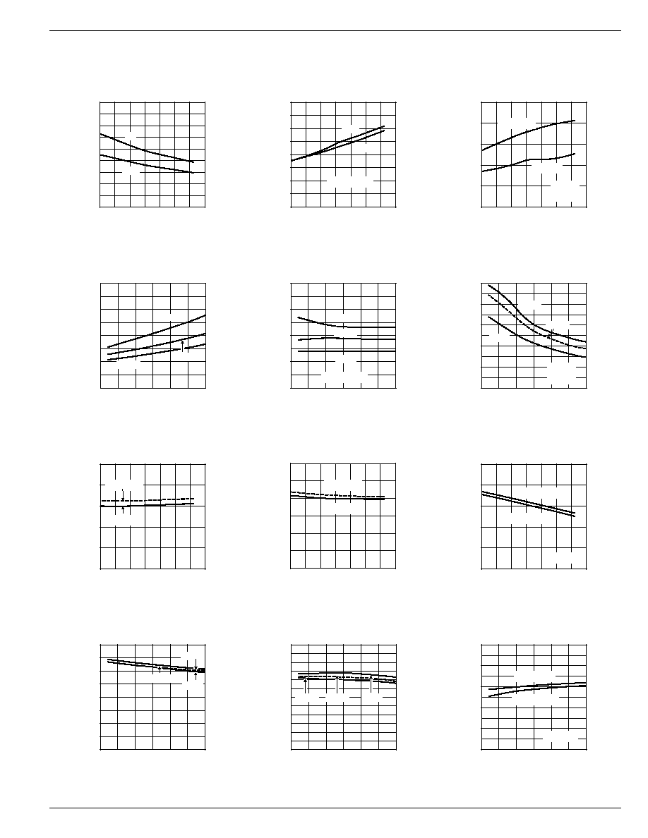
March 2000
5
MIC2025/2075
MIC2025/2075
Micrel
0
20
40
60
80
100
120
140
160
180
-40 -20
0
20
40
60
80 100
CURRENT (
µ
A)
TEMPERATURE (
∞
C)
Supply On-Current
vs. Temperature
5V
3.3V
0
20
40
60
80
100
120
140
160
-40 -20
0
20
40
60
80 100
ON-RESISTANCE (m
)
TEMPERATURE (
∞
C)
On-Resistance
vs. Temperature
5V
3.3V
I
OUT
= 500mA
0
50
100
150
200
2.5
3.0
3.5
4.0
4.5
5.0
5.5
RESISTANCE (m
)
INPUT VOLTAGE (V)
On-Resistance
vs. Input Voltage
I
OUT
= 500mA
+85
∞
C
+25
∞
C
-40
∞
C
0
1
2
3
4
5
-40 -20
0
20
40
60
80 100
RISE TIME (ms)
TEMPERATURE (
∞
C)
Turn-On Rise Time
vs. Temperature
R
L
=10
C
L
=1
µ
F
V
IN
= 5V
V
IN
= 3.3V
0
50
100
150
200
2.5
3.0
3.5
4.0
4.5
5.0
5.5
CURRENT (
µ
A)
INPUT VOLTAGE (V)
Supply On-Current
vs. Input Voltage
+85
∞
C
+25
∞
C
-40
∞
C
0
200
400
600
800
1000
1200
-40 -20
0
20
40
60
80 100
CURRENT LIMIT THRESHOLD (mA)
TEMPERATURE (
∞
C)
Current-Limit Threshold
vs. Temperature
V
IN
= 3.3V
V
IN
= 5V
0
200
400
600
800
1000
-40 -20
0
20
40
60
80 100
CURRENT LIMIT (mA)
TEMPERATURE (
∞
C)
Short-Circuit Current-Limit
vs. Temperature
V
IN
= 3.3V
V
IN
= 5V
0
1.0
2.0
3.0
4.0
5.0
2.5
3.0
3.5
4.0
4.5
5.0
5.5
RISE TIME (ms)
INPUT VOLTAGE (V)
Turn-On Rise Time
vs. Input Voltage
R
L
=10
C
L
=1
µ
F
+85
∞
C
+25
∞
C
-40
∞
C
0
100
200
300
400
500
600
700
800
2.5
3.0
3.5
4.0
4.5
5.0
5.5
CURRENT LIMIT (mA)
INPUT VOLTAGE (V)
Short-Circuit Current-Limit
vs. Input Voltage
+85
∞
C
+25
∞
C
-40
∞
C
0
100
200
300
400
500
600
700
800
900
1000
1100
1200
2.5
3.0
3.5
4.0
4.5
5.0
5.5
CURRENT LIMIT THRESHOLD (mA)
INPUT VOLTAGE (V)
Current-Limit Threshold
vs. Input Voltage
+85
∞
C
+25
∞
C
-40
∞
C
0
0.5
1.0
1.5
2.0
2.5
2.5
3.0
3.5
4.0
4.5
5.0
5.5
ENABLE THRESHOLD (V)
INPUT VOLTAGE (V)
Enable Threshold
vs. Input Voltage
T
A
= 25
∞
C
V
EN
FALLING
V
EN
RISING
0
0.5
1.0
1.5
2.0
2.5
-40 -20
0
20
40
60
80 100
ENABLE THRESHOLD (V)
TEMPERATURE (
∞
C)
Enable Threshold
vs. Temperature
V
IN
= 5V
V
EN
RISING
V
EN
FALLING
MIC2025/2075
Micrel
MIC2025/2075
6
March 2000
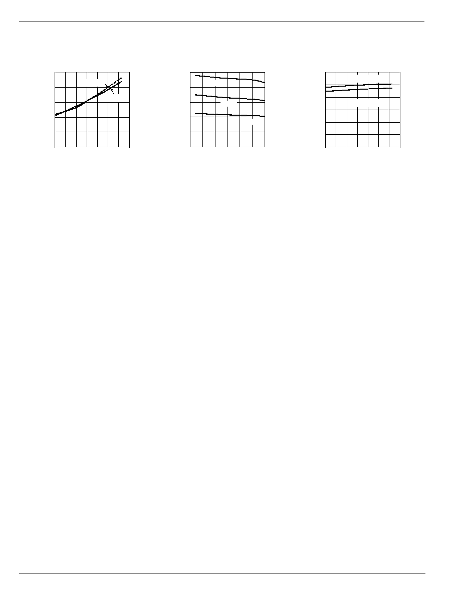
0
1
2
3
4
5
-40 -20
0
20
40
60
80 100
DELAY TIME (ms)
TEMPERATURE (
∞
C)
Flag Delay
vs. Temperature
V
IN
= 3.3V
V
IN
= 5V
0
1
2
3
4
5
2.5
3.0
3.5
4.0
4.5
5.0
5.5
DELAY TIME (ms)
INPUT VOLTAGE (V)
Flag Delay
vs. Input Voltage
+85
∞
C
+25
∞
C
-40
∞
C
0
0.5
1.0
1.5
2.0
2.5
3.0
-40 -20
0
20
40
60
80 100
UVLO THRESHOLD (V)
TEMPERATURE (
∞
C)
UVLO Threshold
vs. Temperature
V
IN
RISING
V
IN
FALLING
March 2000
7
MIC2025/2075
MIC2025/2075
Micrel
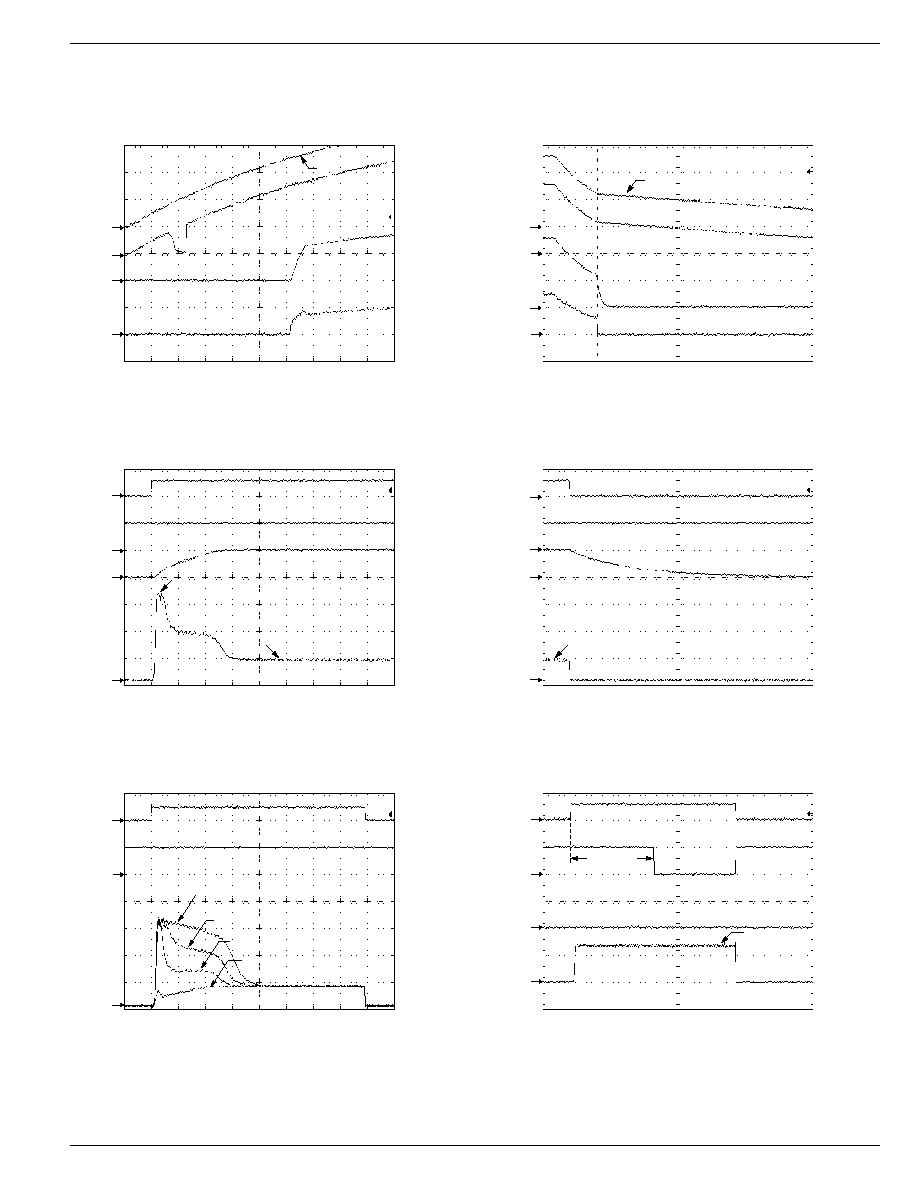
Functional Characteristics
UVLO--V
IN
Rising
(MIC2025-1)
TIME (10ms/div.)
I
OUT
(100mA/div
.
)
V
IN
(1V/div
.
)
V
OUT
(2V/div
.
)
V
FLG
(1V/div
.
)
V
EN
= V
IN
V
IN
= 5V
C
L
= 57
µ
F
R
L
= 35
2.5V
UVLO--V
IN
Falling
(MIC2025-1)
TIME (25ms/div.)
I
OUT
(100mA/div
.
)
V
IN
(2V/div
.
)
V
OUT
(2V/div
.
)
V
FLG
(2V/div
.
)
V
EN
= V
IN
V
IN
= 5V
C
L
= 57
µ
F
R
L
= 35
2.3V
Turn-On Response
(MIC2025-1)
TIME (1ms/div.)
I
OUT
(200mA/div
.
)
V
EN
(10V/div
.
)
V
OUT
(5V/div
.
)
V
FLG
(5V/div
.
)
V
IN
= 5V
C
L
= 147
µ
F
R
L
= 35
640mA
144mA
Inrush Current Response
(MIC2025-1)
TIME (1ms/div.)
I
OUT
(200mA/div
.
)
V
EN
(10V/div
.
)
V
FLG
(5V/div
.
)
V
IN
= 5V
R
L
= 35
C
L
= 310
µ
F
C
L
= 210
µ
F
C
L
= 110
µ
F
C
L
= 10
µ
F
Enable Into Short
(MIC2025-1)
TIME (1ms/div.)
I
OUT
(500mA/div
.
)
V
EN
(10V/div
.
)
V
OUT
(2V/div
.
)
V
FLG
(5V/div
.
)
V
IN
= 5V
3.1ms (t
D
)
640mA
Short-Circuit
Current
Turnoff Response
(MIC2025-1)
TIME (2.5ms/div.)
I
OUT
(200mA/div
.
)
V
EN
(10V/div
.
)
V
OUT
(5V/div
.
)
V
FLG
(5V/div
.
)
V
IN
= 5V
C
L
= 147
µ
F
R
L
= 35
144mA
MIC2025/2075
Micrel
MIC2025/2075
8
March 2000
Current-Limit Response
(Ramped Load Into Short--MIC2025-1)
TIME (100ms/div.)
I
OUT
(500mA/div
.
)
V
IN
(10V/div
.
)
V
OUT
(5V/div
.
)
V
FLG
(5V/div
.
)
V
IN
= 5V
C
L
= 47
µ
F
Current-Limit
Threshold
(780mA)
Thermal
Shutdown
Short-Circuit
Current (650mA)
Short Removed
Current-Limit Transient Response
(Enable Into Short--MIC2025-1)
TIME (500
µ
s/div.)
I
OUT
(5A/div
.
)
V
OUT
(5V/div
.
)
V
FLG
(5V/div
.
)
V
IN
= 5V
C
L
= 47
µ
F
640mA
Short-Circuit Current
Load
No
Load
Current-Limit Transient Response
(MIC2025-1)
TIME (10
µ
s/div.)
I
OUT
(5A/div
.
)
V
OUT
(5V/div
.
)
V
IN
= 5V
C
L
= 47
µ
F
640mA
Short-Circuit Current
24
µ
s
Load
No
Load
Thermal Shutdown Response
(Output Reset by Removing Load--MIC2075-1)
TIME (100ms/div.)
I
OUT
(500mA/div
.
)
V
EN
(10V/div
.
)
V
OUT
(5V/div
.
)
V
FLG
(5V/div
.
)
Thermal
Shutdown
Output is Reset
(Load Removed)
Ramped Load to a Short
Output
Latched Off
V
IN
= 5V
Thermal Shutdown
(Output Reset by Toggling Enable--MIC2075-1)
TIME (100ms/div.)
I
OUT
(500mA/div
.
)
V
EN
(10V/div
.
)
V
OUT
(5V/div
.
)
V
FLG
(5V/div
.
)
Thermal
Shutdown
Enable Reset
Output Reset
R
L
= 35
Ramped Load to a Short
R
L
= 35
V
IN
= 5V
March 2000
9
MIC2025/2075
MIC2025/2075
Micrel
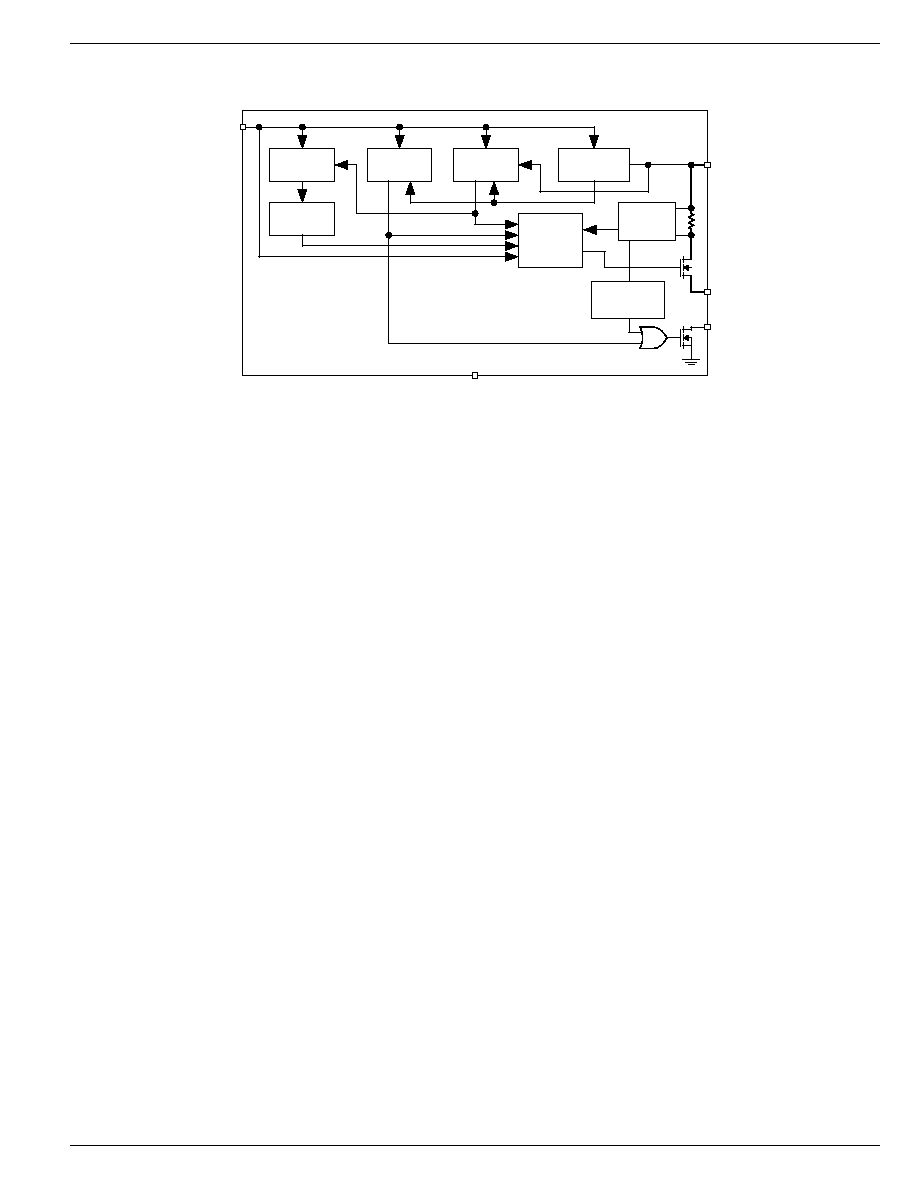
Block Diagram
1.2V
REFERENCE
THERMAL
SHUTDOWN
OSC.
CHARGE
PUMP
OUT
UVLO
GATE
CONTROL
IN
FLG
EN
CURRENT
LIMIT
GND
FLAG
RESPONSE
DELAY
Functional Description
Input and Output
IN is the power supply connection to the logic circuitry and the
drain of the output MOSFET. OUT is the source of the output
MOSFET. In a typical circuit, current flows from IN to OUT
toward the load. If V
OUT
is greater than V
IN
, current will flow
from OUT to IN since the switch is bidirectional when en-
abled. The output MOSFET and driver circuitry are also
designed to allow the MOSFET source to be externally forced
to a higher voltage than the drain (V
OUT
> V
IN
) when the
switch is disabled. In this situation, the MIC2025/75 avoids
undesirable current flow from OUT to IN.
Thermal Shutdown
Thermal shutdown is employed to protect the device from
damage should the die temperature exceed safe margins
due mainly to short circuit faults. Each channel employs its
own thermal sensor. Thermal shutdown shuts off the output
MOSFET and asserts the FLG output if the die temperature
reaches 140
∞
C. The MIC2025 will automatically reset its
output should the die temperature cool down to 120
∞
C. The
MIC2025 output and FLG signal will continue to cycle on and
off until the device is disabled or the fault is removed. Figure
2 depicts typical timing. If the MIC2075 goes into thermal
shutdown, its output will latch off and a pull-up current source
is activated. This allows the output latch to automatically reset
when the load (such as a USB device) is removed. The output
can also be reset by toggling EN. Refer to Figure 1 for details.
Depending on PCB layout, package, ambient temperature,
etc., it may take several hundred milliseconds from the
incidence of the fault to the output MOSFET being shut off.
The worst-case scenario of thermal shutdown is that of a
short-circuit fault and is shown in the in the "Function Char-
acteristics: Thermal Shutdown Response" graph.
Power Dissipation
The device's junction temperature depends on several fac-
tors such as the load, PCB layout, ambient temperature and
package type. Equations that can be used to calculate power
dissipation of each channel and junction temperature are
found below.
P
D
= R
DS(on)
◊
I
OUT
2
Total power dissipation of the device will be the summation of
P
D
for both channels. To relate this to junction temperature,
the following equation can be used:
T
J
= P
D
◊
JA
+ T
A
where:
T
J
= junction temperature
T
A
= ambient temperature
JA
= is the thermal resistance of the package
Current Sensing and Limiting
The current-limit threshold is preset internally. The preset
level prevents damage to the device and external load but still
allows a minimum current of 500mA to be delivered to the
load.
The current-limit circuit senses a portion of the output MOS-
FET switch current. The current-sense resistor shown in the
block diagram is virtual and has no voltage drop. The reaction
to an overcurrent condition varies with three scenarios:
Switch Enabled into Short-Circuit
If a switch is enabled into a heavy load or short-circuit, the
switch immediately enters into a constant-current mode,
reducing the output voltage. The FLG signal is asserted
indicating an overcurrent condition. See the Short-Circuit
Response graph under Functional Characteristics.
MIC2025/2075
Micrel
MIC2025/2075
10
March 2000
Short-Circuit Applied to Enabled Output
When a heavy load or short-circuit is applied, a large transient
current may flow until the current-limit circuitry responds.
Once this occurs the device limits current to less than the
short-circuit current limit specification. See the Short-Circuit
Transient Response graph under Functional Characteristics.
Current-Limit Response--Ramped Load
The MIC2025/75 current-limit profile exhibits a small foldback
effect of about 200mA. Once this current-limit threshold is
exceeded the device switches into a constant current mode.
It is important to note that the device will supply current until
the current-limit threshold is exceeded. See the Current-Limit
Response graph under Functional Characteristics.
Fault Flag
The FLG signal is an N-channel open-drain MOSFET output.
FLG is asserted (active-low) when either an overcurrent or
thermal shutdown condition occurs. In the case where an
overcurrent condition occurs, FLG will be asserted only after
the flag response delay time, t
D
, has elapsed. This ensures
that FLG is asserted only upon valid overcurrent conditions
and that erroneous error reporting is eliminated. For ex-
ample, false overcurrent conditions can occur during hot-plug
events when a highly capacitive load is connected and
causes a high transient inrush current that exceeds the
current-limit threshold. The FLG response delay time t
D
is
typically 3ms.
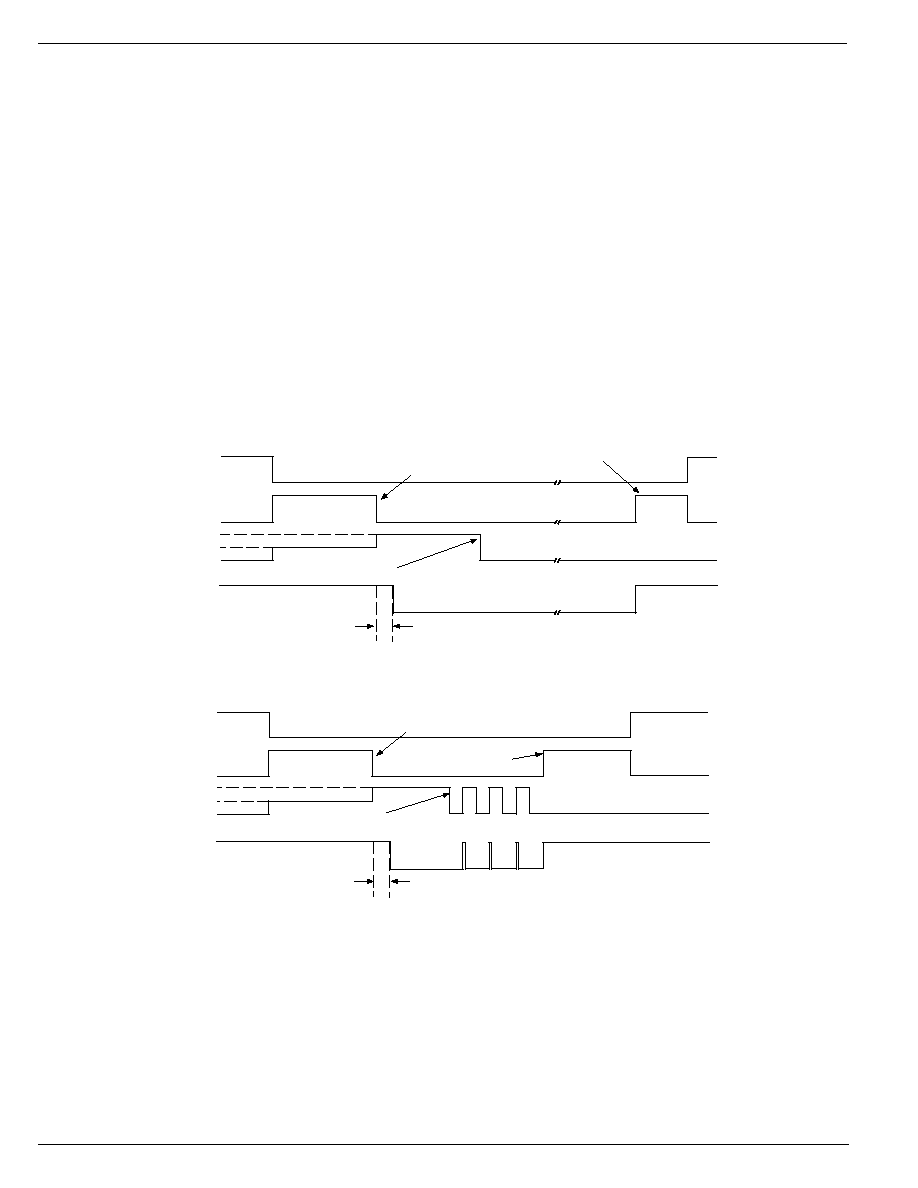
Undervoltage Lockout
Undervoltage lockout (UVLO) prevents the output MOSFET
from turning on until V
IN
exceeds approximately 2.5V. Under-
voltage detection functions only when the switch is enabled.
V
EN
V
OUT
I
OUT
Short-Circuit Fault
Thermal Shutdown
Reached
Load Removed
(Output Reset)
V
FLG
I
LIMIT
I
DC
t
D
Figure 1. MIC2075-2 Timing: Output Reset by Removing Load
V
EN
V
OUT
I
OUT
Short-Circuit Fault
Thermal Shutdown
Reached
Load/Fault
Removed
V
FLG
I
DC
I
LIMIT
t
D
Figure 2. MIC2025-2 Timing
March 2000
11
MIC2025/2075
MIC2025/2075
Micrel
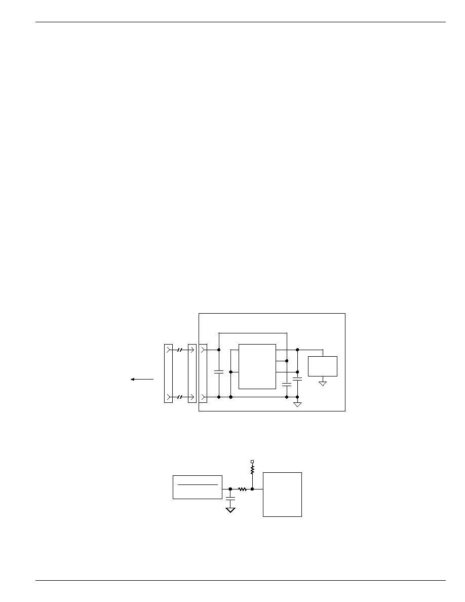
Applications Information
Supply Filtering
A 0.1
µ
F to 1
µ
F bypass capacitor positioned close to V
IN
and
GND of the device is strongly recommended to control supply
transients. Without a bypass capacitor, an output short may
cause sufficient ringing on the input (from supply lead induc-
tance) to damage internal control circuitry.
Printed Circuit Board Hot-Plug
The MIC2025/75 are ideal inrush current-limiters suitable for
hot-plug applications. Due to the integrated charge pump,
the MIC2025/75 presents a high impedance when off and
slowly becomes a low impedance as it turns on. This "soft-
start" feature effectively isolates power supplies from highly
capacitive loads by reducing inrush current during hot-plug
events. Figure 3 shows how the MIC2075 may be used in a
hot-plug application.
In cases of extremely large capacitive loads (>400
µ
F), the
length of the transient due to inrush current may exceed the
delay provided by the integrated filter. Since this inrush
current exceeds the current-limit delay specification, FLG will
be asserted during this time. To prevent the logic controller
from responding to FLG being asserted, an external RC filter,
as shown in Figure 4, can be used to filter out transient FLG
assertion. The value of the RC time constant will be selected
to match the length of the transient.
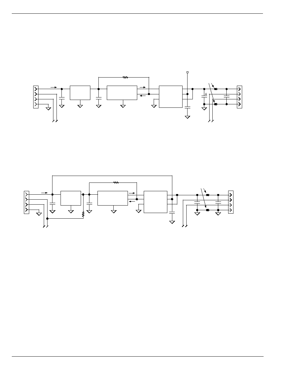
Universal Serial Bus (USB) Power Distribution
The MIC2025/75 is ideally suited for USB (Universal Serial
Bus) power distribution applications. The USB specification
defines power distribution for USB host systems such as PCs
and USB hubs. Hubs can either be self-powered or bus-
powered (that is, powered from the bus). Figure 5 below
shows a typical USB Host application that may be suited for
mobile PC applications employing USB. The requirements
for USB host systems is that the port must supply a minimum
of 500mA at an output voltage of 5V
±
5%. In addition, the
output power delivered must be limited to below 25VA. Upon
an overcurrent condition, the host must also be notified. To
support hot-plug events, the hub must have a minimum of
120
µ
F of bulk capacitance, preferably low-ESR electrolytic or
tantulum. Refer to Application Note 17 for more details on
designing compliant USB hub and host systems.
For bus-powered hubs, USB requires that each downstream
port be switched on or off under control by the host. Up to four
downstream ports each capable of supplying 100mA at 4.4V
minimum are allowed. In addition, to reduce voltage droop on
the upstream V
BUS
, soft-start is necessary. Although the hub
can consume up to 500mA from the upstream bus the hub
must consume only 100mA max at start-up, until it enumer-
ates with the host prior to requesting more power. The same
requirements apply for bus-powered peripherals that have no
downstream ports. Figure 6 shows a bus-powered hub.
MIC2025-2
EN
OUT
FLG
GND
OUT
NC
IN
1
8
2
7
3
6
5
NC
4
Adaptor Card
to "Hot"
Receptacle
C
BULK
GND
V
CC
0.1
µF
Backend
Function
Figure 3. Hot Plug Application
10k
V+
MIC2025
EN
OUT
FLG
GND
OUT
NC
NC
IN
1
8
2
7
3
6
4
5
OVERCURRENT
Logic Controller
R
C
Figure 4. Transient Filter
MIC2025/2075
Micrel
MIC2025/2075
12
March 2000
V
BUS
D+
D≠
GND
USB
Port
Data
EN
OUT
FLG
IN
ON/OFF
OVERCURRENT
MIC2025/75
3.3V USB Controller
GND
OUT
NC
V
CC
5.0V
0.1µF
10k
IN
OUT
GND
4.50V to 5.25V
Upstream V
BUS
100mA max.
Ferrite
Beads
120µF
V
BUS
D+
D≠
GND
Data
1µF
1µF
VIN
GND
3.3V
NC
MIC5203-3.3
0.01µF
Figure 5 USB Host Application
V
BUS
D+
D≠
GND
USB Downstream
Connector
(Up to four
ganaged ports)
Data
EN
OUT
FLG
IN
ON/OFF
OVERCURRENT
MIC2025/75
USB Logic Controller
GND
OUT
NC
0.1µF
1.5k
IN
OUT
GND
USB Upstream
Connector
Ferrite
Beads
120µF
V
BUS
D+
D≠
GND
Data
0.1µF
0.1µF
VIN
GND
3.3V
NC
MIC5203-3.3
(LDO)
0.01µF
1.5K
Figure 6. USB Bus-Powered Hub

March 2000
13
MIC2025/2075
MIC2025/2075
Micrel
Package Information
45
∞
0
∞
≠8
∞
0.244 (6.20)
0.228 (5.79)
0.197 (5.0)
0.189 (4.8)
SEATING
PLANE
0.026 (0.65)
MAX
)
0.010 (0.25)
0.007 (0.18)
0.064 (1.63)
0.045 (1.14)
0.0098 (0.249)
0.0040 (0.102)
0.020 (0.51)
0.013 (0.33)
0.157 (3.99)
0.150 (3.81)
0.050 (1.27)
TYP
PIN 1
DIMENSIONS:
INCHES (MM)
0.050 (1.27)
0.016 (0.40)
8-Lead SOP (M)
0.008 (0.20)
0.004 (0.10)
0.039 (0.99)
0.035 (0.89)
0.021 (0.53)
0.012 (0.03) R
0.0256 (0.65) TYP
0.012 (0.30) R
5
∞
MAX
0
∞
MIN
0.122 (3.10)
0.112 (2.84)
0.120 (3.05)
0.116 (2.95)
0.012 (0.03)
0.007 (0.18)
0.005 (0.13)
0.043 (1.09)
0.038 (0.97)
0.036 (0.90)
0.032 (0.81)
DIMENSIONS:
INCH (MM)
0.199 (5.05)
0.187 (4.74)
MM8TM 8-Pin MSOP (MM)

MIC2025/2075
Micrel
MIC2025/2075
14
March 2000

March 2000
15
MIC2025/2075
MIC2025/2075
Micrel

MIC2025/2075
Micrel
MIC2025/2075
16
March 2000
MICREL INC.
1849 FORTUNE DRIVE
SAN JOSE, CA 95131
USA
TEL
+ 1 (408) 944-0800
FAX
+ 1 (408) 944-0970
WEB
http://www.micrel.com
This information is believed to be accurate and reliable, however no responsibility is assumed by Micrel for its use nor for any infringement of patents or
other rights of third parties resulting from its use. No license is granted by implication or otherwise under any patent or patent right of Micrel Inc.
© 2000 Micrel Incorporated