February 1, 2001
1
MIC2026/2076
MIC2026/2076
Micrel
MIC2026/2026A/2076/2076A
Dual-Channel Power Distribution Switch
General Description
The MIC2026 and MIC2076 are high-side MOSFET switches
optimized for general-purpose power distribution requiring
circuit protection.
The MIC2026/76 are internally current limited and have
thermal shutdown that protects the device and load.
The MIC2076 offers "smart" thermal shutdown that reduces
current consumption in fault modes. When a thermal shut-
down fault occurs, the output is latched off until the faulty load
is removed. Removing the load or toggling the enable input
will reset the device output.
Both devices employ soft-start circuitry that minimizes inrush
current in applications where highly capacitive loads are
employed.
A fault status output flag is asserted during overcurrent and
thermal shutdown conditions. Transient faults are internally
filtered.
The MIC2026/76 are available in 8-pin DIP or 8-lead SOP.
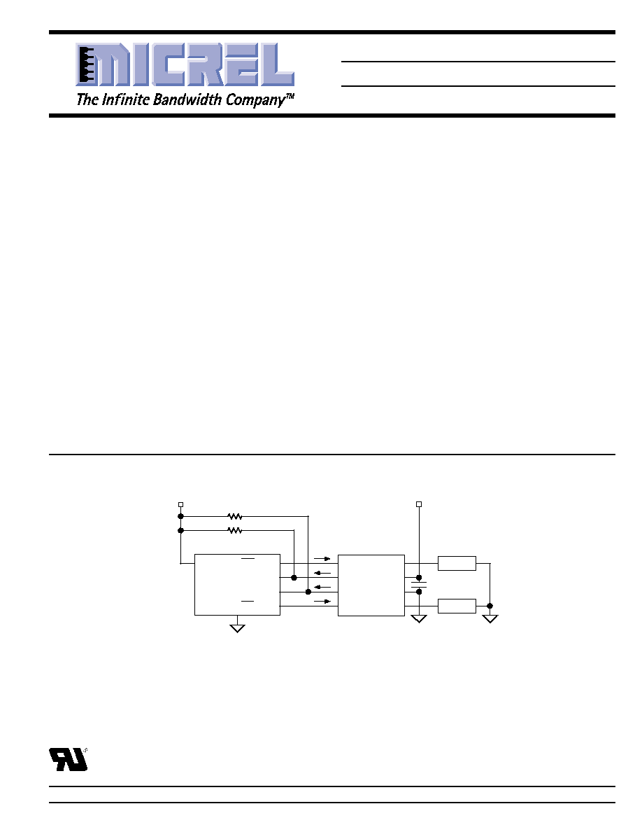
Typical Application
ENA
OUTA
FLGA
IN
FLGB
GND
ENB
OUTB
ON/OFF
OVERCURRENT
OVERCURRENT
ON/OFF
MIC2026-2
Logic Controller
V
CC
2.7V to 5.5V
0.1µF
VIN
Load
Load
V
CONT.
10k
10k
Features
∑ 140m
maximum on-resistance per channel
∑ 2.7V to 5.5V operating range
∑ 500mA minimum continuous current per channel
∑ Shortcircuit protection with thermal shutdown
∑ Thermally isolated channels
∑ Fault status flag with 3ms filter eliminates false asser-
tions (MIC2026A/2076A with 10ms filter)
∑ Undervoltwww.sony.com/clieage lockout
∑ Reverse current flow blocking (no "body diode")
∑ Circuit breaker mode (MIC2076)
∑ Logic-compatible inputs
∑ Soft-start circuit
∑ Low quiescent current
∑ Pin compatible with MIC2526
Applications
∑ USB peripherals
∑ General purpose power switching
∑ ACPI power distribution
∑ Notebook PCs
∑ PDAs
∑ PC card hot swap
Micrel, Inc. ∑ 1849 Fortune Drive ∑ San Jose, CA 95131 ∑ USA ∑ tel + 1 (408) 944-0800 ∑ fax + 1 (408) 944-0970 ∑ http://www.micrel.com
UL Recognized Component
MIC2026/2076
Micrel
MIC2026/2076
2
February 1, 2001
Ordering Information
Part Number
Enable
Temperature Range
Package
MIC2026x-1BM
Active High
≠40
∞
C to +85
∞
C
8-lead SOP
MIC2026x-2BM
Active Low
≠40
∞
C to +85
∞
C
8-lead SOP
MIC2026x-1BN
Active High
≠40
∞
C to +85
∞
C
8-pin DIP
MIC2026x-2BN
Active Low
≠40
∞
C to +85
∞
C
8-pin DIP
MIC2076x-1BM
Active High
≠40
∞
C to +85
∞
C
8-lead SOP
MIC2076x-2BM
Active Low
≠40
∞
C to +85
∞
C
8-lead SOP
MIC2076x-1BN
Active High
≠40
∞
C to +85
∞
C
8-pin DIP
MIC2076x-2BN
Active Low
≠40
∞
C to +85
∞
C
8-pin DIP
Note. x=A; optional part that includes a 10ms Fault status delay filter. No `x' denotes standard part.
Pin Description
Pin Number
Pin Name
Pin Function
1
ENA
Switch A Enable (Input): Logic-compatible enable input. Active high (-1) or
active low (-2).
2
FLGA
Fault Flag A (Output): Active-low, open-drain output. Indicates overcurrent
or thermal shutdown conditions. Overcurrent conditions must last longer
than t
D
in order to assert FLGA.
3
FLGB
Fault Flag B (Output): Active-low, open-drain output. Low indicates
overcurrent or thermal shutdown conditions.Overcurrent conditions must last
longer than t
D
in order to assert FLGB.
4
ENB
Switch B Enable (Input): Logic-compatible enable input. Active-high (-1) or
active-low (-2).
5
OUTB
Switch B (Output)
6
GND
Ground
7
IN
Input: Switch and logic supply input.
8
OUTA
Switch A (Output)
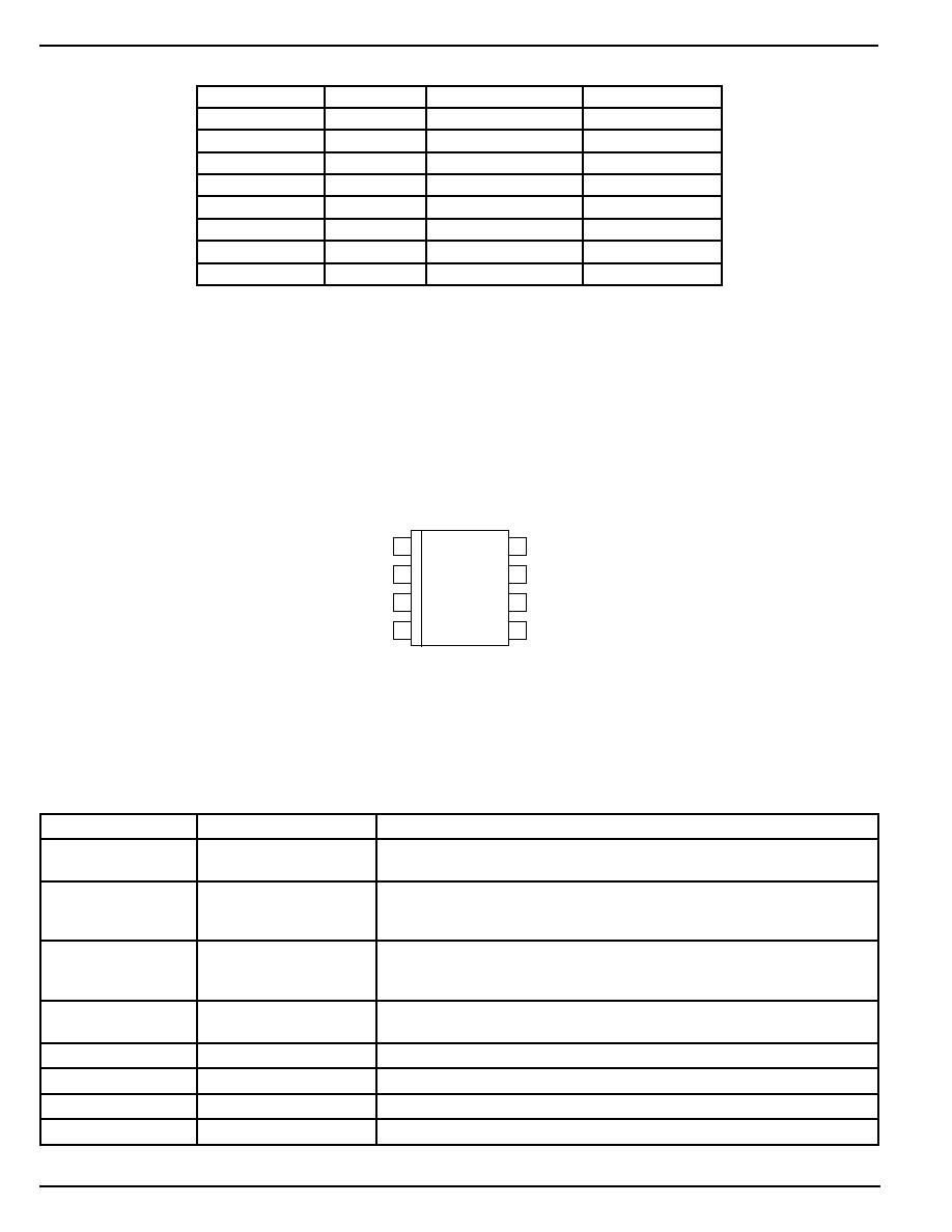
Pin Configuration
1
2
3
4
8
7
6
5
OUTA
IN
GND
OUTB
ENA
FLGA
FLGB
ENB
MIC2026/76
8-Lead SOP (BM)
8-Pin DIP (BN)

February 1, 2001
3
MIC2026/2076
MIC2026/2076
Micrel
Electrical Characteristics
V
IN
= +5V; T
A
= 25
∞
C, bold values indicate ≠40
∞
C
T
A
+85
∞
C; unless noted
Symbol
Parameter
Condition
Min
Typ
Max
Units
I
DD
Supply Current
MIC20x6-1, V
ENA
= V
ENB
0.8V
0.75
5
µ
A
(switch off), OUT = open
MIC20x6-2, V
ENA
= V
ENB
2.4V
0.75
5
µ
A
(switch off), OUT = open
MIC20x6-1, V
ENA
= V
ENB
2.4V
100
160
µ
A
(switch on), OUT = open
MIC20x6-2, V
ENA
= V
ENB
0.8V
100
160
µ
A
(switch on), OUT = open
V
EN
Enable Input Threshold
low-to-high transition
1.7
2.4
V
high-to-low transition
0.8
1.45
V
Enable Input Hysteresis
250
mV
I
EN
Enable Input Current
V
EN
= 0V to 5.5V
≠1
0.01
1
µ
A
Enable Input Capacitance
1
pF
R
DS(on)
Switch Resistance
V
IN
= 5V, I
OUT
= 500mA
90
140
m
V
IN
= 3.3V, I
OUT
= 500mA
100
170
m
Output Leakage Current
MIC20x6-1, V
ENx
0.8V;
10
µ
A
MIC20x6-1, V
ENx
2.4V, (output off)
OFF Current in
MIC2076
50
µ
A
Latched Thermal Shutdown
(during thermal shutdown state)
t
ON
Output Turn-On Delay
R
L
= 10
, C
L
= 1
µ
F, see "Timing Diagrams"
1.3
5
ms
t
R
Output Turn-On Rise Time
R
L
= 10
, C
L
= 1
µ
F, see "Timing Diagrams"
0.5
1.15
4.9
ms
R
L
= 10
, C
L
= 1
µ
F, see "Timing Diagrams"
1.75
ms
MIC2026A/MIC2076A
t
OFF
Output Turn-Off Delay
R
L
= 10
, C
L
= 1
µ
F, see "Timing Diagrams"
35
100
µ
s
t
F
Output Turn-Off Fall Time
R
L
= 10
, C
L
= 1
µ
F, see "Timing Diagrams"
32
100
µ
s
I
LIMIT
Short-Circuit Output Current
V
OUT
= 0V, enabled into short-circuit
0.5
0.9
1.25
A
Current-Limit Threshold
ramped load applied to output
1.0
1.25
A
Short-Circuit Response Time
V
OUT
= 0V to I
OUT
= I
LIMIT
20
µ
s
(short applied to output)
t
D
Overcurrent Flag Response
V
IN
= 5V, apply V
OUT
= 0V until FLG low
1.5
3
7
ms
Delay
V
IN
= 3.3V, apply V
OUT
= 0V until FLG l ow
3
ms
V
IN
= 5V, apply V
OUT
= 0V until FLG low
10
ms
MIC2026A/MIC2076A
Absolute Maximum Ratings
(Note 1)
Supply Voltage (V
IN
) ...................................... ≠0.3V to +6V
Fault Flag Voltage (V
FLG
) .............................................. +6V
Fault Flag Current (I
FLG
) ............................................ 25mA
Output Voltage (V
OUT
) .................................................. +6V
Output Current (I
OUT
) ............................... Internally Limited
Enable Input (I
EN
) .................................... ≠0.3V to V
IN
+ 3V
Storage Temperature (T
S
) ...................... ≠65
∞
C to +150
∞
C
ESD Rating, Note 3
Operating Ratings
(Note 2)
Supply Voltage (V
IN
) ................................... +2.7V to +5.5V
Ambient Temperature (T
A
) ......................... ≠40
∞
C to +85
∞
C
Junction Temperature Range (T
J
) ........... Internally Limited
Thermal Resistance
SOP (
JA
) .......................................................... 160
∞
C/W
DIP(
JA
) ............................................................. 105
∞
C/W

MIC2026/2076
Micrel
MIC2026/2076
4
February 1, 2001
Symbol
Parameter
Condition
Min
Typ
Max
Units
Undervoltage Lockout
V
IN
rising
2.2
2.4
2.7
V
Threshold
V
IN
falling
2.0
2.15
2.5
V
Error Flag Output
I
L
= 10mA, V
IN
= 5V
10
25
Resistance
I
L
= 10mA, V
IN
= 3.3V
15
40
Error Flag Off Current
V
FLAG
= 5V
10
µ
A
Overtemperature Threshold
T
J
increasing, each switch
140
∞
C
Note 4
T
J
decreasing, each switch
120
∞
C
T
J
increasing, both switches
160
∞
C
T
J
decreasing, both switches
150
∞
C
Note 1.
Exceeding the absolute maximum rating may damage the device.
Note 2.
The device is not guaranteed to function outside its operating rating.
Note 3.
Devices are ESD sensitive. Handling precautions recommended.
Note 4.
If there is a fault on one channel, that channel will shut down when the die reaches approximately 140
∞
C. If the die reaches approximately
160
∞
C, both channels will shut down, even if neither channel is in current limit.
Test Circuit
Device
Under
Test
C
L
OUT
R
L
V
OUT
Timing Diagrams
90%
V
OUT
10%
90%
10%
t
R
t
F
Output Rise and Fall Times
V
EN
50%
90%
V
OUT
10%
t
OFF
t
ON
Active-Low Switch Delay Times (MIC20x6-2)
V
EN
50%
90%
V
OUT
10%
t
OFF
t
ON
Active-High Switch Delay Times (MIC20x6-1)

February 1, 2001
5
MIC2026/2076
MIC2026/2076
Micrel
0
20
40
60
80
100
120
140
160
180
-40 -20
0
20
40
60
80 100
CURRENT (
µ
A)
TEMPERATURE (
∞
C)
Supply On-Current
vs. Temperature
5V
3.3V
0
20
40
60
80
100
120
140
160
-40 -20
0
20
40
60
80 100
ON-RESISTANCE (m
)
TEMPERATURE (
∞
C)
On-Resistance
vs. Temperature
5V
3.3V
I
OUT
= 500mA
0
1
2
3
4
5
-40 -20
0
20
40
60
80 100
RISE TIME (ms)
TEMPERATURE (
∞
C)
Turn-On Rise Time
vs. Temperature
R
L
=10
C
L
=1
µ
F
V
IN
= 5V
V
IN
= 3.3V
0
50
100
150
200
2.5
3.0
3.5
4.0
4.5
5.0
5.5
CURRENT (
µ
A)
INPUT VOLTAGE (V)
Supply On-Current
vs. Input Voltage
+85
∞
C
+25
∞
C
-40
∞
C
0
50
100
150
200
2.5
3.0
3.5
4.0
4.5
5.0
5.5
RESISTANCE (m
)
INPUT VOLTAGE (V)
On-Resistance
vs. Input Voltage
I
OUT
= 500mA
+85
∞
C
+25
∞
C
-40
∞
C
0
0.5
1.0
1.5
2.0
2.5
2.5
3.0
3.5
4.0
4.5
5.0
5.5
RISE TIME (ms)
INPUT VOLTAGE (V)
Turn-On Rise Time
vs. Input Voltage
R
L
=10
C
L
=1
µ
F
+85
∞
C
+25
∞
C
-40
∞
C
0
200
400
600
800
1000
-40 -20
0
20
40
60
80 100
CURRENT LIMIT (mA)
TEMPERATURE (
∞
C)
Short-Circuit Current-Limit
vs. Temperature
V
IN
= 3.3V
V
IN
= 5V
0
200
400
600
800
1000
1200
-40 -20
0
20
40
60
80 100
CURRENT LIMIT THRESHOLD (mA)
TEMPERATURE (
∞
C)
Current-Limit Threshold
vs. Temperature
V
IN
= 3.3V
V
IN
= 5V
0
100
200
300
400
-40 -20
0
20
40
60
80 100
FALL TIME (
µ
s)
TEMPERATURE (
∞
C)
Fall Time
vs. Temperature
R
L
=10
C
L
=1
µ
F
V
IN
= 3.3V
0
100
200
300
400
500
600
700
800
2.5
3.0
3.5
4.0
4.5
5.0
5.5
CURRENT LIMIT (mA)
INPUT VOLTAGE (V)
Short-Circuit Current-Limit
vs. Input Voltage
+85
∞
C
+25
∞
C
-40
∞
C
0
200
400
600
800
1000
1200
2.5
3.0
3.5
4.0
4.5
5.0
5.5
CURRENT LIMIT THRESHOLD (mA)
INPUT VOLTAGE (V)
Current-Limit Threshold
vs. Input Voltage
+85
∞
C
+25
∞
C
-40
∞
C
0
50
100
150
200
250
300
2.5
3.0
3.5
4.0
4.5
5.0
5.5
RISE TIME (
µ
s)
INPUT VOLTAGE (V)
Fall Time
vs. Input Voltage
T
A
= 25
∞
C
C
L
= 1
µ
F
R
L
= 10