October 2003
1
MIC2044/2045
MIC2044/2045
Micrel
MIC2044/2045
Single Channel, High Current, Low Voltage,
Protected Power Distribution Switch
General Description
The MIC2044 and MIC2045 are high-side MOSFET switches
optimized for general purpose power distribution applications
that require circuit protection. These devices switch up to
5.5V and as low as 0.8V while offering both programmable
current limiting and thermal shutdown to protect the device
and the load. A fault status output is provided to indicate
overcurrent and thermal shutdown fault conditions. Both
devices employ soft-start circuitry to minimize the inrush
current in applications that employ highly capacitive loads.
Additionally, for tighter control over inrush current during start
up, the output slew-rate may be adjusted by an external
capacitor.
The MIC2045 features a auto-reset circuit breaker that latches
the output OFF upon detecting an overcurrent condition
lasting more than 32ms. The output is reset by removing or
reducing the load.
Data sheets and support documentation can be found on
Micrel's web site at www.micrel.com.
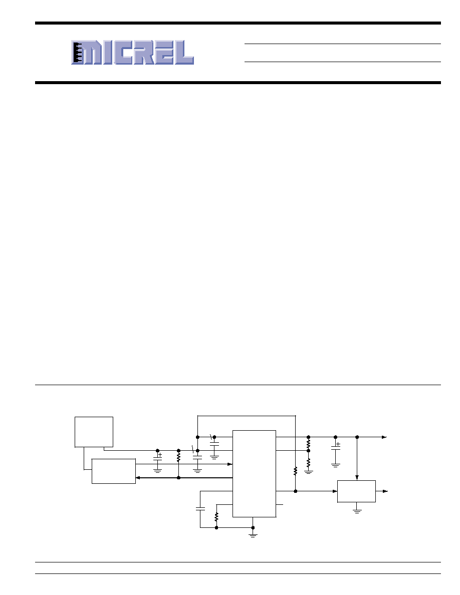
Typical Application
7, 11,
13, 16
8
2
3
6
4
15
9,12,14
1
5
R
SET
100W
Note:
All V
IN
pins (7, 11, 13, 16) must be externally tied together.
All V
OUT
pins (9, 12, 14) must be externally tied together.
I
LIMIT
= 4A.
Output Power-Good = 3.0V.
*C4 is optional. See
"Applications Information."
C4*
0.022mF
C1
0.1mF
Logic
Controller
ON/OFF
OVERCURRENT
IN
10
MIC2044-1BTS
MIC39100-2.5BS
VBIAS
VIN
EN
/FAULT
ILIM
SLEW
2.5V
VOUT
PGREF
PWRGD
UVLOIN
GND
R1
20kW
R2
294kW
1%
R3
24.3kW
1%
EN
IN
GND
OUT
C
LOAD
33mF
V
OUT
3.3V@ 3.5A
R4
20kW
(OPEN)
+3.3V
Power
Supply
OUT1
OUT2
C3
4.7mF
C2
0.1mF
Features
∑ 30m
maximum on-resistance
∑ 0.8V to 5.5V operating range
∑ Adjustable current limit
∑ Up to 6A continuous output current
∑ Short circuit protection
∑ Very fast reaction to short circuits
∑ Thermal shutdown
∑ Adjustable slew-rate control
∑ Circuit breaker mode (MIC2045)
∑ Fault status flag
∑ Power-Good detection
∑ Undervoltage lockout
∑ No reverse current flow through the switching MOSFET
when OFF or disabled
∑ Low quiescent current
Applications
∑ Docking stations
∑ LAN servers
∑ WAN switches
∑ Hot swap board insertions
∑ Notebook PCs
∑ PDAs
∑ Base stations
∑ RAID controllers
∑ USB hosts
Micrel, Inc. ∑ 1849 Fortune Drive ∑ San Jose, CA 95131 ∑ USA ∑ tel + 1 (408) 944-0800 ∑ fax + 1 (408) 944-0970 ∑ http://www.micrel.com

MIC2044/2045
Micrel
MIC2044/2045
2
October 2003
Pin Configuration
1
PWRGD
EN
/FAULT
SLEW
UVLOIN
ILIM
VIN
VBIAS
16 VIN
PGREF
VOUT
VIN
VOUT
VIN
GND
VOUT
15
14
13
12
11
10
9
2
3
4
5
6
7
8
MIC2044/MIC2045
16-Pin TSSOP (TS)
Ordering Information
Part Number
Enable
Circuit Breaker
Package
MIC2044-1BTS
Active-High
16-Pin TSSOP
MIC2044-2BTS
Active-Low
16-Pin TSSOP
MIC2045-1BTS
Active-High
X
16-Pin TSSOP
MIC2045-2BTS
Active-Low
X
16-Pin TSSOP

October 2003
3
MIC2044/2045
MIC2044/2045
Micrel
Pin Description
Pin Number
Pin Name
Pin Function
1
PWRGD
Power-Good (Output): Open drain N-Channel device, active high. This pin
asserts high when the voltage at PGREF exceeds its threshold.
2
EN
Switch Enable (Input): Gate control pin of the output MOSFET available as
an active high (≠1) or active low (≠2) input signal.
3
/FAULT
Fault Status (Output): Open drain N-Channel device, active low. This pin
indicates an overcurrent or thermal shutdown condition. For an overcurrent
event, /FAULT is asserted if the duration of the overcurrent condition lasts
longer than 32ms.
10
GND
Ground connection: Tie to analog ground.
4
SLEW
Slew-Rate Control (Input): A capacitor connected between this pin and
ground will reduce (slow) the output slew-rate. The output turn-on time must
be less than the nominal flag delay of 32ms in order to avoid nuisance
tripping of the /FAULT output since V
OUT
must be "fully on" (i.e., within
200mV of the voltage at the input) before the /FAULT signal delay elapses.
The slew-rate limiting capacitor requires a 16V rating or greater, 25V is
recommended. See
"Applications Information: Output Slew-Rate Adjust-
ment"
for further details.
6
ILIM
Current Limit (Input): A resistor (R
SET
) connected from this pin to ground
sets the current limit threshold as I
LIMIT
= CLF/R
SET
. CLF is the current limit
factor specified in the
"Electrical Characteristics"
table. For the MIC2044/45,
the continuous output current range is 1A to 6A.
5
UVLOIN
Undervoltage Lockout Adjust (Input): With this pin left open, the UVLO
threshold is internally set to 1.45V. When the switching voltage (V
IN
) is at or
below 1.5V, connecting an external resistive divider to this input will lower the
UVLO threshold. The total resistance of the divider must be less than 200k
.
To disable the UVLO, tie this pin to VIN. See
"Applications Information"
for
further detail.
7,11,13,16
VIN
Switch Supply (Input): Connected to the drain of the output MOSFET. The
range of input for the switch is 0.8V to 5.5V. These pins must be externally
connected together to achieve rated performance.
9,12,14
VOUT
Switch (Output): Connected to the source of the output MOSFET. These
pins must be externally connected together to achieve rated performance.
8
VBIAS
Bias Supply (Input): This input pin supplies power to operate the switch and
internal circuitry. The input range for VBIAS is 1.6V to 5.5V. When switched
voltage (V
IN
) is between 1.6V to 5.5V and the use of a single supply is
desired, connect VBIAS to VIN externally.
15
PGREF
Power-Good Threshold (Input): Analog reference used to specify the
PWRGD threshold. When the voltage at this pin exceeds its threshold, V
TH
,
PWRGD is asserted high. An external resistive divider network is used to
determine the output voltage level at which V
TH
is exceeded. See the
"Functional Description"
for further detail. When the PWRGD signal is not
utilized, this input should be tied to VOUT.

MIC2044/2045
Micrel
MIC2044/2045
4
October 2003
Absolute Maximum Ratings
(Note 1)
V
IN
and V
BIAS ..................................................................................
6V
/FAULT, PWRGD Output Voltage ................................... 6V
/FAULT, PWRGD Output Current .............................. 25mA
ESD Rating, Note 3
Human Body Model ................................................... 2kV
Machine Model ........................................................ 200V
Operating Ratings
(Note 2)
Supply Voltage
V
IN
............................................................... 0.8V to 5.5V
V
BIAS
........................................................... 1.6V to 5.5V
Continuous Output Current ................................... 1A to 6A
Ambient Temperature (T
A
) ........................... ≠40
∞
C to 85
∞
C
Package Thermal Resistance
(
R
(J-A)
)
TSSOP ................................................................ 85
∞
C/W
Electrical Characteristics
(Note 4)
V
IN
= V
BIAS
= 5V, T
A
= 25
∞
C unless specified otherwise. Bold indicates ≠40
∞
C to +85
∞
C.
Symbol
Parameter
Condition
Min
Typ
Max
Units
V
IN
Switch Input Voltage
V
IN
V
BIAS
0.8
5.5
V
V
BIAS
Bias Supply Voltage
1.6
5.5
V
I
BIAS
V
BIAS
Supply Current - Switch OFF
No load
0.1
5
µ
A
V
BIAS
Supply Current - Switch ON
No load
300
400
µ
A
Note 5
V
EN
Enable Input Voltage
V
IL(max)
2.4
1.5
V
V
IH(min)
3.5
2.5
V
V
ENHYST
Enable Input Threshold Hysteresis
100
mV
I
EN
Enable Input Current
V
EN
= 0V to 5.5V
≠1
.01
1
µ
A
R
DS(ON)
Switch Resistance
V
IN
= V
BIAS
= 3V, 5V
20
30
m
I
OUT
= 500mA
I
LEAK
Output Leakage Current
Output off
10
µ
A
CLF
Current Limit Factor
V
IN
= 3V, 5V, 0.5V
V
OUT
< 0.5V
IN
300
380
460
A∑
Note 6
1A
I
OUT
6A
V
TH
PGREF Threshold
V
IN
= V
BIAS
= 1.6V to 5.5V
215
230
245
mV
V
LATCH
Output Reset Threshold
V
IN
= 0.8V to 5.5V
V
IN
≠.0.2
V
V
OUT
rising (MIC2045)
I
LATCH
Latched Output Off Current
Output latched off (MIC2045)
1
3
5
mA
V
OL
Output Low Voltage
I
OL
(/FAULT) = 15mA
0.4
V
(/FAULT, PWRGD)
I
OL
(PWRGD) = 5mA
I
OFF
/FAULT, PWRGD Off Current
V
FAULT
= V
PWRGD
= 5V
1
µ
A
V
UV
Undervoltage Lockout Threshold
V
IN
rising
1.30
1.45
1.58
V
V
IN
falling
1.20
1.35
1.50
V
V
UVHYST
Undervoltage Lockout
100
mV
Threshold Hysteresis
V
UVINTH
UVLO Adjust Pin Threshold Voltage
V
IN
rising
200
230
260
mV
V
IN
falling
185
215
245
mV
V
UVINHYST
UVLO Adjust Pin Threshold Hysteresis
15
mV
Overtemperature Threshold
T
J
increasing
140
∞
C
T
J
decreasing
120
∞
C
October 2003
5
MIC2044/2045
MIC2044/2045
Micrel
Symbol
Parameter
Condition
Min
Typ
Max
Units
t
FLAG
Flag Response Delay
V
IN
= V
BIAS
= 3V, 5V
25
32
40
ms
t
ON
Output Turn-on Delay
R
LOAD
= 10
, C
LOAD
= 1
µ
F
0.75
1
1.25
ms
t
R
Output Turn-on Rise Time
R
LOAD
= 10
, C
LOAD
= 1
µ
F
1.5
2.5
3.5
ms
t
OFF
Output Turn-off Delay
R
LOAD
= 10
, C
LOAD
= 1
µ
F
1
5
µ
s
t
F
Output Turn-off Fall Time
R
LOAD
= 10
, C
LOAD
= 1
µ
F
24
µ
s
Note 1.
Exceeding the absolute maximum rating may damage the device.
Note 2.
The device is not guaranteed to function outside its operating rating.
Note 3.
Devices are ESD sensitive. Handling precautions recommended. Human body model: 1.5k
in series with 100pF.
Note 4.
Specification for packaged product only.
Note 5.
OFF is V
EN
< 1.0V for MIC2044/MIC2045≠1 and V
EN
> 4.0V for MIC2044/MIC2045 ≠2. ON is V
EN
> 4.0V for MIC2044/MIC2045≠1 and
V
EN
< 1.0V for MIC2044/MIC2045 ≠2.
Note 6.
The current limit is determined as follows: I
LIM
= CLF/R
SET
.
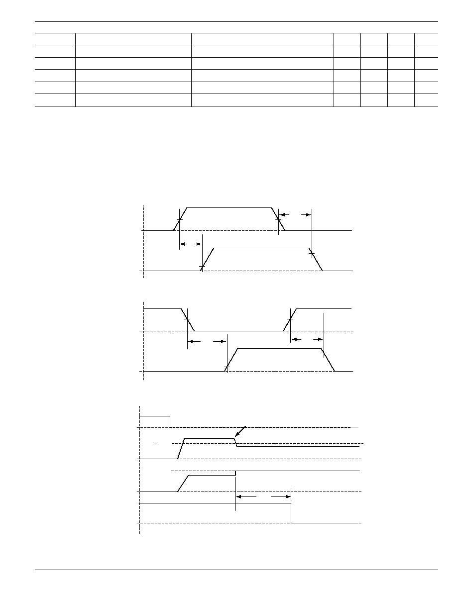
Timing Diagrams
50%
(a) MIC2044/45-1
(b) MIC2044/45-2
10%
90%
0
V
EN
t
ON
t
OFF
0
V
OUT
50%
10%
90%
0
V
EN
t
ON
t
OFF
0
V
OUT
Figure 1. Turn-On/Turn-Off Delay
0
V
EN
I
LIMIT
0
V
OUT
0
I
OUT
0
/FAULT
t
FLAG
V
IN
0.2V
Increase the load
Figure 2. Overcurrent Fault Response -- MIC2044-2
MIC2044/2045
Micrel
MIC2044/2045
6
October 2003
Test Circuit
7, 11,
13, 16
8
2
3
5
4
15
9,12,14
1
6
*R
SET
*R
SET
and C
SLEW
use multiple values
(See specific response plots)
*C
SLEW
C2
0.1
µ
F
10
MIC2044/45-xBTS
VBIAS
VIN
EN
/FAULT
UVLOIN
SLEW
VOUT
PGREF
PWRGD
ILIM
GND
R2
20k
R1
20k
R5
260k
R6
24k
C
LOAD
47
µ
F
V
OUT
I
LOAD
R7
20k
C3
10
µ
F
C1
0.1
µ
F
V
IN
V
DD
R3
75k
R4
68k
October 2003
7
MIC2044/2045
MIC2044/2045
Micrel
100
125
150
175
200
225
250
275
300
-40 -20
0
20
40
60
80 100
SUPPLY CURRENT (
µ
A)
TEMPERATURE (
∞
C)
Supply Current
vs. Temperature
V
IN
= V
BIAS
= 1.6V
V
IN
= V
BIAS
= 5.5V
V
IN
= V
BIAS
= 3V
0
1
2
3
4
5
-40 -20
0
20
40
60
80 100
V
EN
(V)
TEMPERATURE (
∞
C)
Enable Input Threshold
(Rising)
vs. Temperature
V
BIAS
= 5.5V
V
BIAS
= 3V
V
BIAS
= 1.6V
0
1
2
3
4
5
-40 -20
0
20
40
60
80 100
V
EN
(V)
TEMPERATURE (
∞
C)
Enable Input Threshold
(Falling)
vs. Temperature
V
BIAS
= 5.5V
V
BIAS
= 3V
V
BIAS
= 1.6V
0
250
500
750
1000
1250
1500
1750
2000
2250
2500
-40 -20
0
20
40
60
80 100
OUTPUT LEAKAGE (nA)
TEMPERATURE (
∞
C)
Output Leakage Current
vs. Temperature
V
BIAS
= 5.5V
V
BIAS
= 3V
V
BIAS
= 1.6V
0
5
10
15
20
25
30
35
40
-40 -20
0
20
40
60
80 100
ON RESISTANCE (m
)
TEMPERATURE (
∞
C)
ON Resistance
vs. Temperature
V
IN
= V
BIAS
= 1.6V
V
IN
= V
BIAS
= 3V
V
IN
= V
BIAS
= 5.5V
20
25
30
35
40
45
50
-40 -20
0
20
40
60
80 100
T
FLAG
(ms)
TEMPERATURE (
∞
C)
Flag Response Delay
vs. Temperature
T
FLAG
= 3V
T
FLAG
= 5V
200
400
600
800
1000
1200
1400
1600
-40 -20
0
20
40
60
80 100
TURN ON DELAY (
µ
s)
TEMPERATURE (
∞
C)
Turn On Delay
vs. Temperature
V
IN
= V
BIAS
= 5.5V
V
IN
= V
BIAS
= 3V
V
IN
= V
BIAS
= 1.6V
0
5
10
15
20
25
0
1
2
3
4
5
6
I
R
(mA)
V
OUT
≠V
BIAS
(V)
V
BIAS
Reverse Current Flow
vs. Output Voltage
V
IN
= GND
V
BIAS
= 1.6V
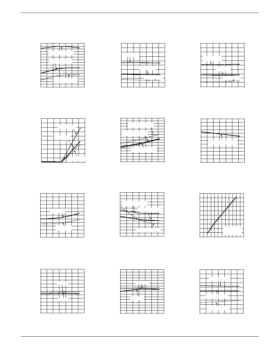
Typical Characteristics
0
0.5
1
1.5
2
2.5
3
-40 -20
0
20
40
60
80 100
UVLO THRESHOLD (V)
TEMPERATURE (
∞
C)
UVLO Threshold
vs. Temperature
UVLO+
UVLO≠
0
50
100
150
200
250
300
350
400
-40 -20
0
20
40
60
80 100
UVLOIN THRESHOLD (mV)
TEMPERATURE (
∞
C)
UVLO Adjust Pin Threshold
vs. Temperature
UVLOIN+
UVLOIN≠
0
5
10
15
20
25
-40 -20
0
20
40
60
80 100
SLEW PIN VOLTAGE (V)
TEMPERATURE (
∞
C)
SLEW Voltage
vs. Temperature
V
IN
= V
BIAS
= 1.6V
V
IN
= V
BIAS
= 5V
V
IN
= V
BIAS
= 3V
210
215
220
225
230
-40 -20
0
20
40
60
80 100
V
TH
(mV)
TEMPERATURE (
∞
C)
Power-Good Reference
Threshold
vs. Temperature
V
TH
@ 1.6V to 5.5V
MIC2044/2045
Micrel
MIC2044/2045
8
October 2003
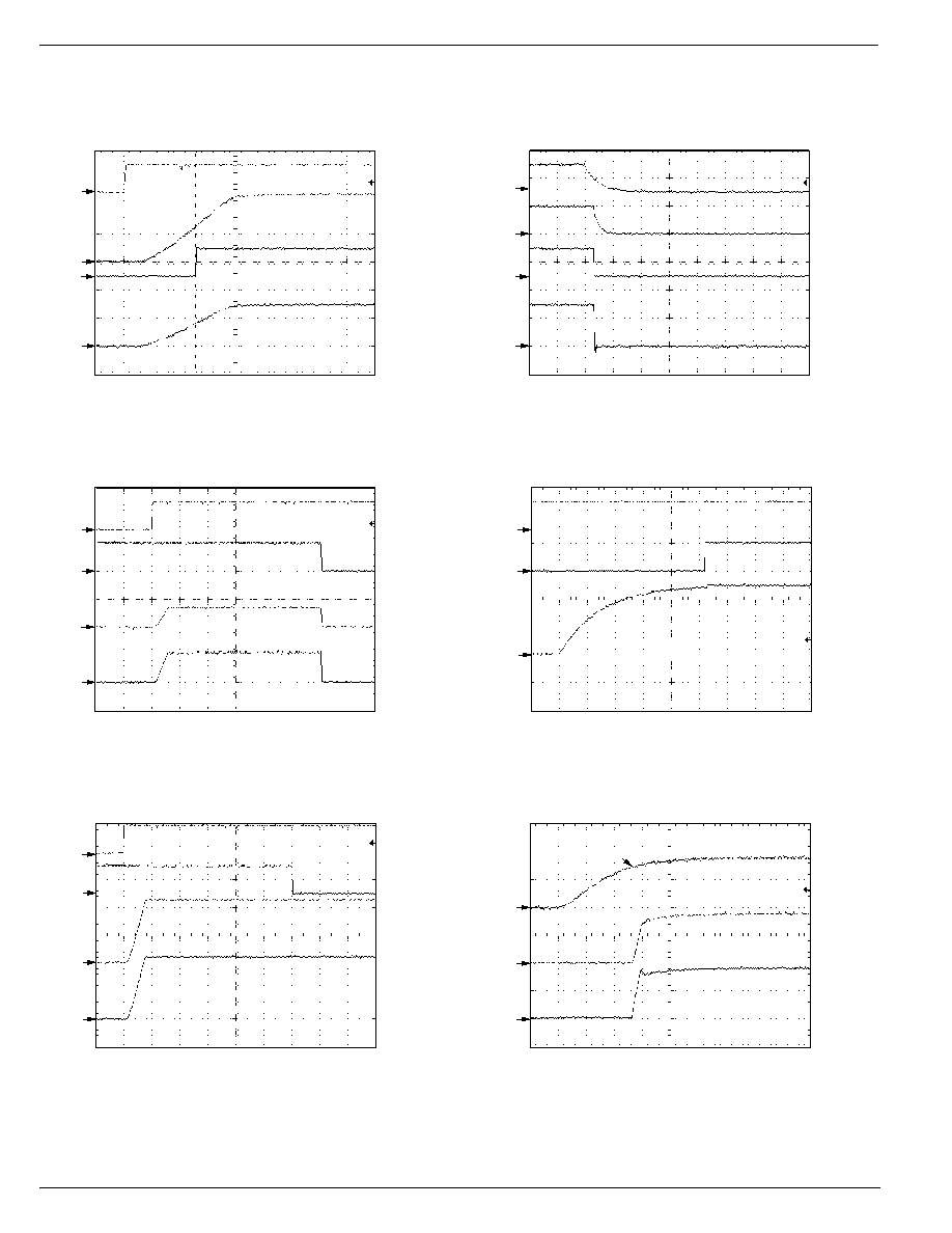
Functional Characteristics
I
OUT
2A/div
PWRGD 5V/div
V
OUT
2V/div
EN
5V/div
V
IN
= V
BIAS
= 5.0V
R
LOAD
= 1.65W
C
LOAD
= 47mF
R
SET
= 100W
5V Turn-On
TIME (1ms/div.)
I
OUT
2A/div
PWRGD 5V/div
V
OUT
5V/div
EN
5V/div
V
IN
= V
BIAS
= 5.0V
R
LOAD
= 1.65V
C
LOAD
= 47mF
R
SET
= 100W
5V Turn-Off
TIME (500ms/div.)
I
OUT
2A/div
V
OUT
5V/div
/F
AUL
T
5V/div
EN
5V/div
V
IN
= V
BIAS
=
5.0V
R
LOAD
=
1.8
C
LOAD
=
47
µ
F
R
SET
=
220
Latched Output
MIC2045
TIME (5ms/div.)
V
OUT
2V/div
/F
AUL
T
5V/div
EN
5V/div
V
IN
= V
BIAS
=
5.0V
R
LOAD
toggles from 2
to OPEN
C
LOAD
=
47
µ
F
R
SET
=
220
4.82V
Latched Output Reset
MIC2045
TIME (50ms/div.)
I
OUT
200mA/div
V
IN
1V/div
V
OUT
1V/div
V
IN
ramps 0V to 1.8V
R
LOAD
=
5
C
LOAD
=
47
µ
F
R
SET
=
220
UVLO Response
TIME (2.5ms/div.)
1.45V
I
OUT
2A/div
/F
AUL
T
5V/div
EN
5V/div
V
OUT
2V/div
V
IN
= V
BIAS
=
5.0V
R
LOAD
=
1.2
C
LOAD
=
47
µ
F
R
SET
=
100
Current Limit Response
TIME (5ms/div.)
October 2003
9
MIC2044/2045
MIC2044/2045
Micrel
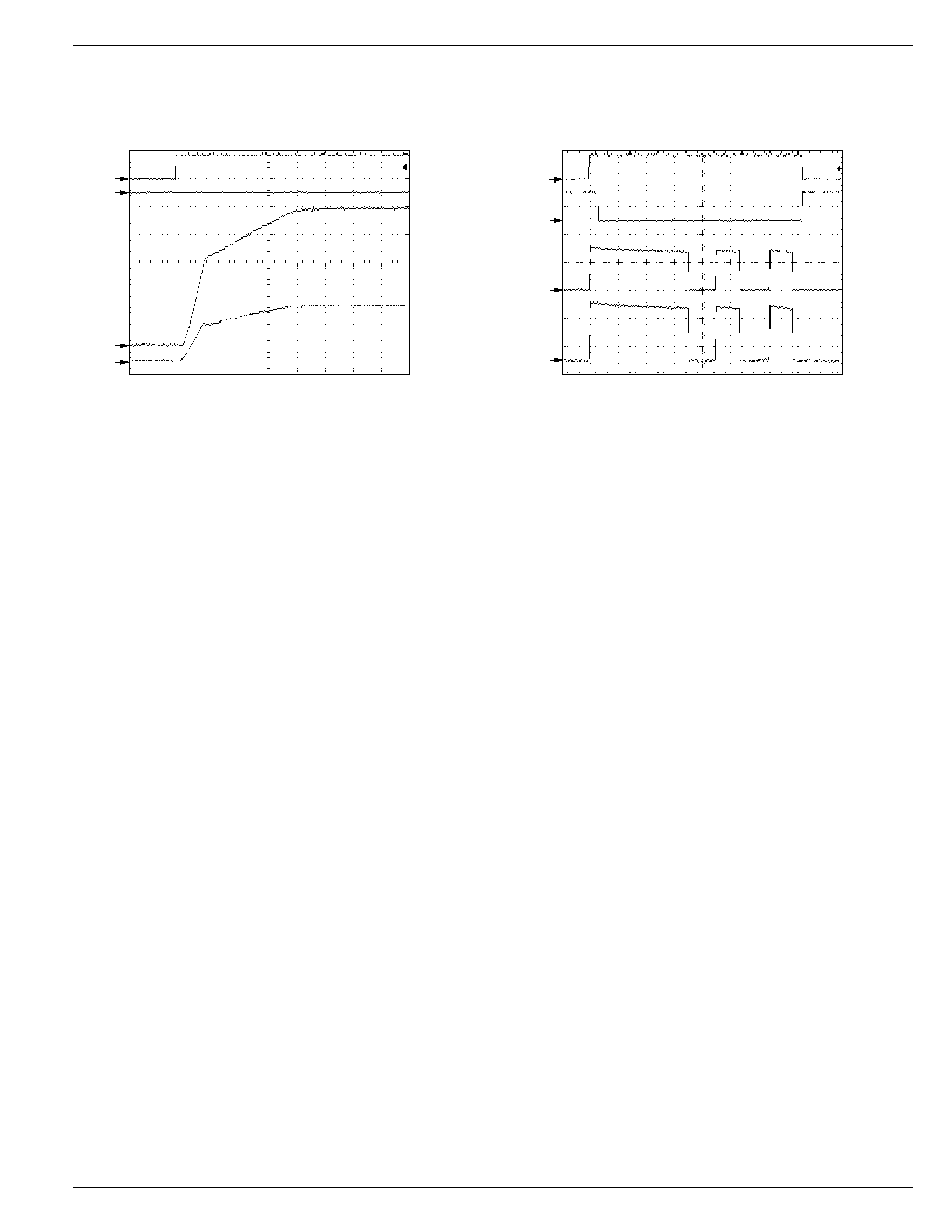
Functional Characteristics (continued)
V
OUT
1V/div
/F
AUL
T
5V/div
EN
5V/div
I
OUT
500mA/div
V
IN
= 5.0V
R
LOAD
=
5
C
LOAD
=
47
µ
F
C
SLEW
=
0.033
µ
F
R
SET
=
220
Output Slew Response
TIME (2.5ms/div.)
V
OUT
2V/div
/F
AUL
T
5V/div
EN
5V/div
I
OUT
1A/div
V
IN
= V
BIAS
5.0V
R
LOAD
=
2
C
LOAD
=
47
µ
F
R
SET
=
220
Thermal Shutdown Response
TIME (100ms/div.)
MIC2044/2045
Micrel
MIC2044/2045
10
October 2003
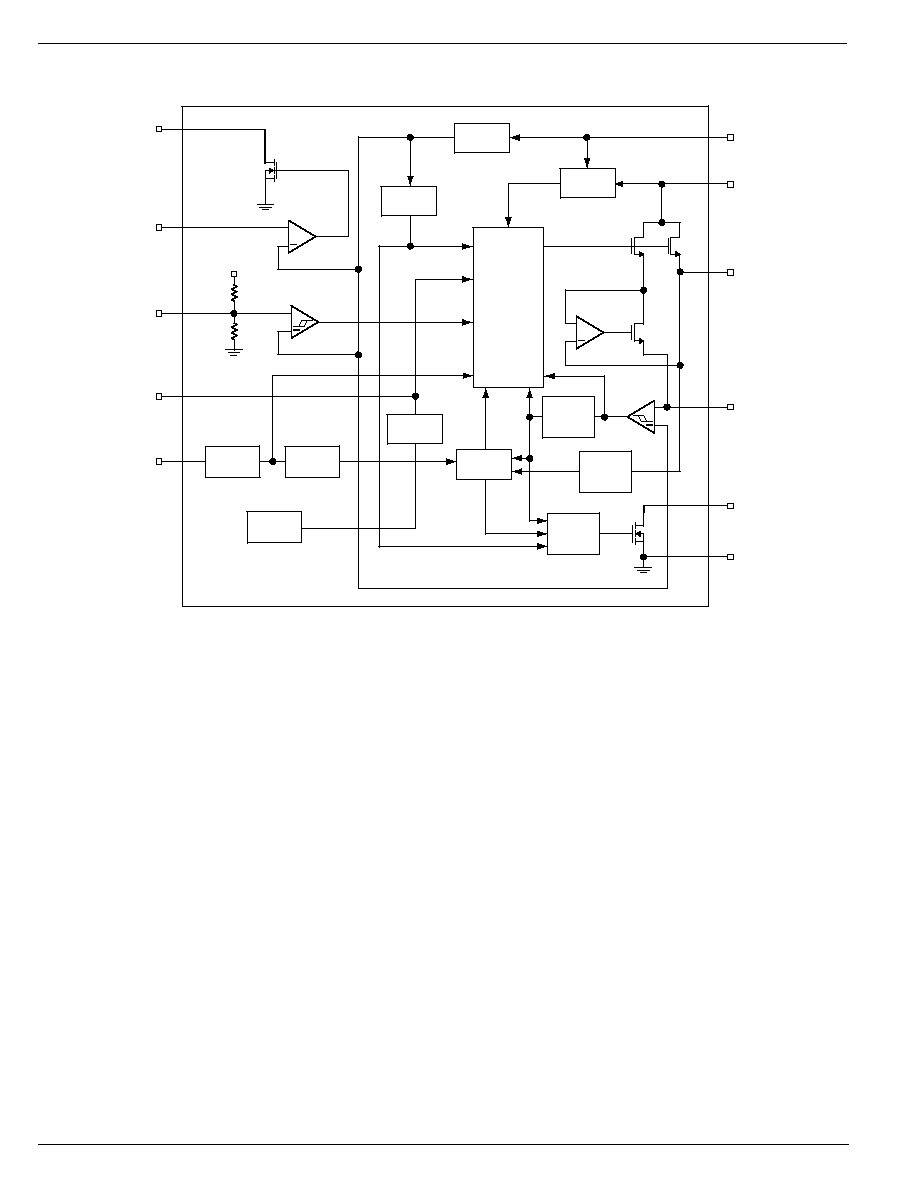
Functional Diagram
MIC2044/45
Bandgap
Reference
OSC
UVLO
5.3x
1x
V
REF
= 230mV
Current
Limit
Replica
Amp
+
+
V
IN
ILIM
6
VOUT
9,12,14
VBIAS
8
VIN
7,11,13,16
/FAULT
3
GND
10
+
Gate
Control
UVLOIN
5
SLEW
4
EN
2
PGREF
15
Open
Load
Detect
I
LIM
Delay
(32ms)
PWRGD
1
+
Error
Flag
Logic
Power-On
Reset
Input
Logic
Latch
(MIC2045)
Charge
Pump
Thermal
Shutdown
Power-Off
Reset

October 2003
11
MIC2044/2045
MIC2044/2045
Micrel
Functional Description
The MIC2044 and MIC2045 are high-side N-Channel switches
equipped with programmable current limit up to 6A for use in
general purpose power distribution applications. The switches,
available with active-high or active-low enable inputs, provide
output slew-rate control and circuit protection via thermal
shutdown and an optional output latch during overcurrent
conditions.
Input and Output
VBIAS supplies power to the internal circuitry of the switch
and must be present for the switch to operate. VIN is con-
nected to the drain of the output MOSFET and sources power
to the switched load. VIN must be less than or equal to VBIAS.
VOUT is the source terminal of the output MOSFET and
attaches to the load. In a typical circuit, current flows from VIN
to VOUT toward the load. If VOUT is greater than VIN, current
will flow from VOUT to VIN since the switch is bi-directional
when the device is enabled. When disabled (OFF), the switch
will block current flow from either direction.
Enable Input
Enable, the ON/OFF control for the output switch, is a digital
input available as an active-high (≠1) or active-low (≠2)
signal. The EN pin, referenced to approximately 0.5
◊
VBIAS,
must be driven to a clearly defined logic high or logic low.
Failure to observe this requirement, or allowing EN to float,
will cause the MIC2044/45 to exhibit unpredictable behavior.
EN should not be allowed to go negative with respect to
ground, nor allowed to exceed VBIAS. Failure to adhere to
these conditions may result in damage to the device.
Undervoltage Lockout
When the switch is enabled, undervoltage lockout (UVLO)
monitors the input voltage, V
IN
, and prevents the output
MOSFET from turning on until V
IN
exceeds a predetermined
level, nominally set at 1.45V. The UVLO threshold is adjust-
able and can be varied by applying an external resistor divider
to the UVLOIN pin from VIN to GND. The resistive divider
network is required when the input voltage is below 1.5V. The
UVLO threshold is internally preset to 1.45V if the UVLOIN
pin is left open. See
"Applications Information."
Programmable Current Limit
The MIC2044/45 is designed to prevent damage to the
external load by limiting the maximum amount of current it
can draw. The current limit is programmed by an external
resistor (R
SET
) connected from ILIM (Pin 6) to ground and
becomes active when the output voltage is at least 200mV
below the voltage at the input to the device. The limiting
current value is defined by the current limit factor (CLF)
divided by R
SET
, and the MIC2044/45 will limit from 1A to 6A
with a set point accuracy of
±
21%. In programming the
nominal current limit, the value of R
SET
is determined using
the following equation:
R
CLF
I
380A
I
SET
LIMIT
LIMIT
=
=
◊
(
)
(1)
And given the
±
21% tolerance of the current limit factor (CLF),
the external resistor is bound by:
50
R
SET
460
(2)
The graphs below (Figure 3) display the current limit factor
characteristic over the full temperature range at the indicated
voltage. These curves can be used as a point of reference in
determining the maximum variation in the device's current
limit over the full temperature range. For example: With V
IN
= V
BIAS
= 3.0V and a nominal 4A current limit (R
SET
= 95
),
the low and high current limit settings for the MIC2044/45
would be 3.15A and 4.85A, respectively, as shown on the 3V
graph using the 95
reference point.
When current limiting occurs, the MIC2044 and MIC2045
respond differently. Upon first reaching the limiting current
both devices restrict current flow, allowing the load voltage to
drop below V
IN
. If the V
IN
to V
OUT
differential voltage exceeds
200mV, then a fault condition is declared and the fault delay
timer is started. If the fault condition persists longer than the
delay period, typically 32ms, then the /FAULT output asserts
low. At this point, the MIC2044 will continue to supply current
to the load at the limiting value (I
LIMIT
), whereas the MIC2045
will latch off its output.
0
1
2
3
4
5
6
7
8
0
50 100 150 200 250 300 350 400 450
I
LIMIT
(A)
R
SET
(
)
Current Limit
vs. R
SET
≠40
∞
C to +85
∞
C
V
IN
= V
BIAS
= 3V, 5V
CLF (LO)
CLF (HI)
0
1
2
3
4
5
6
7
8
0
50 100 150 200 250 300 350 400 450
I
LIMIT
(A)
R
SET
(
)
Current Limit
vs. R
SET
≠40
∞
C to +85
∞
C
V
IN
= V
BIAS
= 1.6V
CLF (LO)
CLF (HI)
Figure 3. Current Limit Factor

MIC2044/2045
Micrel
MIC2044/2045
12
October 2003
/FAULT
The /FAULT signal is an N-Channel, open-drain MOSFET
output. An external pull-up resistor tied to a maximum 6V rail
is required for the /FAULT pin. The /FAULT pin is asserted
(active-low) when either an overcurrent or thermal shutdown
condition occurs. During a hot insert of a PCB or when turning
on into a highly capacitive load, the resulting high transient
inrush current may exceed the current limit threshold of the
MIC2044/45. In the case where an overcurrent condition
occurs, /FAULT will assert only after the flag delay time has
elapsed, typically 32ms. This ensures that /FAULT is as-
serted only upon valid overcurrent conditions and that nui-
sance error reporting is prevented.
Thermal Shutdown
For the MIC2044, thermal shutdown is employed to protect
the device from damage should the die temperature exceed
safe margins due to a short circuit or an excessive load.
Thermal shutdown shuts off the output MOSFET and asserts
the /FAULT output if the die temperature exceeds 140
∞
C.
The MIC2044 automatically resets its output and resumes
supplying current to the load when the die temperature drops
to 120
∞
C. If the fault is still present, the MIC2044 will quickly
re-heat and shut down again. This process of turning
ON-OFF-ON is called thermal cycling and will continue as
long as the power switch is enabled while the fault or
excessive load is present.
Depending on PCB layout (including thermal considerations
such as heat sinking), package, and ambient temperature, it
may take several hundred milliseconds from the incidence of
the fault to the output MOSFET being shut off.
Circuit Breaker Function (MIC2045)
The MIC2045 is designed to shut off all power to the load
when a fault condition occurs, just as a circuit breaker would
do. In this case, a fault condition is deemed to be anytime the
output current exceeds the current limit for more than the flag
delay period, nominally 32ms. Once the output shuts off, it
remains off until either the fault load is removed from VOUT
or the EN input is cycled ON-OFF-ON. If the fault is still
present after EN has been cycled, the MIC2045 will again
shut off all power to the load after 32ms. Once the fault has
been removed, then normal operation will resume.
Open Load Detection
The MIC2045 will automatically reset its output when the fault
load is cleared. This is accomplished by applying a small
current to VOUT and watching for the voltage at VOUT to rise
to within 200mV of VIN. This current is supplied by an internal
resistor connected to VIN and is connected to VOUT when
MIC2045 latches off.
Power-Good Detection
The MIC2044/45 can detect when the output voltage is above
or below a preset threshold that is monitored by a comparator
at the PGREF input. The PWRGD signal is an N-Channel
open-drain MOSFET output and an external pull-up resistor
up to a 6V maximum rail is required for the PWRGD pin.
Whenever the voltage at the PGREF pin exceeds its thresh-
old (V
TH
), typically 230mV, the PWRGD output is asserted.
Using the typical applications circuit from page 1 that switches
3.3V as an example, the output voltage threshold determin-
ing "power is good" is calculated by the following equation:
V
V
1
R2
R3
OUT(GOOD)
TH
=
◊ +
(3)
In substituting the resistor values of the circuit and the typical
PGREF threshold, the resulting V
OUT(GOOD)
is calculated as
3.0V for this 3.3V switching application.
SLEW
The MIC2044/45's output rise time is controlled at turn-on to
a minimum of 1.5ms and is controlled by an internal slew-rate
limiting circuit. A slew-rate adjustment control pin is available
for applications requiring slower rise times. By placing a
capacitor between SLEW and ground, longer rise times can
be achieved. For further detail, see the
"Applications Informa-
tion"
section.

October 2003
13
MIC2044/2045
MIC2044/2045
Micrel
Applications Information
Input and Output
Supply Bypass Filtering
The need for input supply bypass is brought about due to
several factors, most notably the input/output inductance
along the power path, operating current and current limit, and
output capacitance. A 0.1
µ
F to 0.47
µ
F bypass capacitor
positioned very close to the VIN pin to GND of the device is
strongly recommended to filter high frequency oscillations
due to inductance. Also, a sufficient bypass capacitor posi-
tioned close to the input source to the switch is strongly
advised in order to suppress supply transient spikes and to
limit input voltage droop. Inrush current increases with larger
output capacitance, thus the minimum value of this capacitor
will require experimental determination for the intended appli-
cation and design. A good starting point is a capacitor
between 4.7
µ
F to 15
µ
F. Without these bypass capacitors, an
extreme overload condition such as a short circuit, or a large
capacitive load, may cause either the input supply to exceed
the maximum rating of 6V and possibly cause damage to the
internal control circuitry or allow the input supply to droop and
fall out of regulation and/or below the minimum operating
voltage of the device.
Output Capacitance
When the MIC2044 die exceeds the overtemperature thresh-
old of approximately 140
∞
C, the device can enter into a
thermal shutdown mode if the die temperature falls below
120
∞
C and then rises above 140
∞
C in a continuous cycle.
With VOUT cycling on and off, the MIC2044 will reset the
/FAULT while in an overtemperature fault condition if V
OUT
is
allowed to swing below ground. The inductance present at
the output must be neutralized by capacitance in order to
ensure that the output does not fall below ground. In order to
counter the board parasitic inductance and the inductance of
relatively short-length power cable (
1ft., 16 - 20 gauge wire),
a minimum output capacitance of 22
µ
F is strongly recom-
mended and should be placed close to the VOUT pin of the
MIC2044. For applications that use more than a foot of cable,
an additional 10
µ
F/ft. is recommended.
Reverse Current Blocking
The MIC2044/45 provides reverse current flow blocking
through the output MOSFET if the voltage at VOUT is greater
than VIN when the device is disabled. The V
BIAS
supply has
a limited reverse current flow if the voltage at VOUT is pulled
above VBIAS when the device is disabled. A graph of the
V
BIAS
reverse current flow is shown in the
"Functional
Characteristics"
section. The reverse current for VBIAS can
be completely blocked by inserting a Schottky diode from the
VBIAS pin (cathode) to the supply (anode). However, the
minimum voltage of 1.6V must be supplied to VBIAS after
accounting for the voltage drop across the diode.
Output Slew-Rate Adjustment
The output slew-rate for the MIC2044/45 can be slowed down
by the use of a capacitor (16V rating, minimum; 25V sug-
gested) between SLEW and GND. The slew-rate control
circuitry is independent of the load capacitance and exhibits
a non-linear response. See the
"Functional Characteristics"
section. Table 1 shows the rise time for various standard
capacitor values. Additionally, the output turn-on time must
be less than the nominal flag delay of 32ms in order to avoid
nuisance tripping of the /FAULT output. This limit is imposed
by the current limiting circuitry which monitors the
(VIN ≠ VOUT) differential voltage and concludes a fault
condition is present if the differential voltage exceeds 200mV
for more than the flag delay period. For the MIC2045, the
/FAULT will assert and the output will latch off if the output is
not within 200mV of the input before the flag delay times out.
When using the active-low (≠2) option with the EN input tied
to ground, slew control is functional during initial start-up but
does not function upon resetting the input power to the
device. In order for the SLEW control to operate during
consecutive system restarts, the EN pin must reset (toggle
OFF to ON).
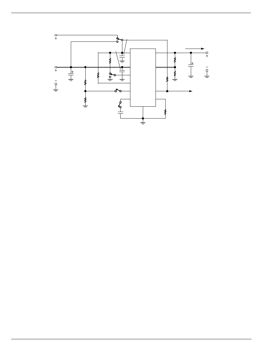
UVLO Threshold Setting With Low Input Voltages
When the switching voltage is below 1.6V, the device's
standard UVLO threshold (1.45V nominal) will hinder the
output MOSFET in switching VIN to VOUT. In this case, the
use of the UVLOIN pin is required to override the standard
UVLO threshold and set a new, lower threshold for the lower
input voltage. An external resistive divider network con-
nected at the UVLOIN pin is used to set the new threshold.
Due to the ratio of the internal components, the total series
resistance of the external resistive divider should not exceed
200k
. The circuit shown in Figure 4 illustrates an application
that switches 0.8V while the device is powered from a
separate 2.5V power supply. The UVLO threshold is set by
the following equation.
V
0.23V
1
R2
R3
UVTH
=
◊ +
(4)
In substituting the resistor values from Figure 4, the resulting
UVLO threshold (V
UVTH
) is calculated as 0.6V for this 0.8V
switching application. When using the UVLOIN pin to set a
new UVLO threshold, an optional 0.1
µ
F to 1.0
µ
F capacitor
from UVLOIN to GND may be used as a glitch filter in order
to avoid nuisance tripping of the UVLO threshold. If the
UVLOIN pin is not in use, this pin should be left open
(floating). The use of a pull-down resistor to ground will offset
the ratio of the internal resistive divider to this pin resulting in
a shift in the UVLO threshold. To bypass (disable) UVLO,
connect the UVLOIN pin directly to the VIN pin of the
MIC2044/45.
Conditions: V
IN
= V
BIAS
= 5V/3V
C
LOAD
= 47
µ
F; I
LOAD
= 1A
C
SLEW
(
µ
F)
Rise Time (ms)
5V
3V
0.02
4.4
6.6
0.033
7.5
11.25
0.047
11
16
0.1
24
31.5
Table 1. Typical Output Rise Time for Various C
SLEW
(V
IN
= 5V, 3V)

MIC2044/2045
Micrel
MIC2044/2045
14
October 2003
7,11,
13,16
8
2
5
4
6
15
9,12,14
1
3
R
SET
200W
C1
0.1mF
10
MIC2044-1BTS
VBIAS
VIN
EN
/FAULT
UVLOIN
SLEW
VOUT
PGREF
PWRGD
ILIM
GND
R1
47kW
R4
75kW
1%
R5
36.5kW
1%
C
LOAD
22mF
V
OUT
0.8V @1.5A
R7
47kW
Digital
Output
Signals
C3
10mF
C2
0.1mF
V
IN
0.8V
V
DD
2.5V
R2
95.3kW
1%
R3
59.0kW
1%
R6
47kW
Note:
All V
IN
pins (7, 11, 13, 16) must be externally tied together.
All V
OUT
pins (9, 12, 14) must be externally tied together.
Undervoltage Lockout = 0.6V.
Output Power-Good = 0.7V.
Figure 4. Lower UVLO Setting
Power Dissipation
Power dissipation depends on several factors such as the
load, PCB layout, ambient temperature, and package type.
The following equations can be used to calculate power
dissipation and die temperature.
Calculation of power dissipation can be accomplished by the
following equation:
P
D
= R
DS(on)
◊
(I
OUT
)
2
(5)
To relate this to junction temperature, the following equation
can be used:
T
J
= P
D
◊
R
(
J-A)
+ T
A
(6)
where T
J
= junction temperature, T
A
= ambient temperature
and R
(J-A)
is the thermal resistance of the package.
Printed Circuit Board Hot Plug
The MIC2044/45 are ideal inrush current limiting power
switches suitable for hot plug applications. Due to the inte-
grated charge pump, the MIC2044/45 present a high imped-
ance when in the off state and the device slowly becomes a
low impedance as it turns on. This effectively isolates power
supplies from highly capacitive loads by reducing inrush
current during hot plug events. This same feature also can be
used for soft-start requirements.
PCB Layout Recommendations
The MIC2044 and MIC2045 have very low on-resistance,
typically 20m
, and the switches can provide up to 6A of
continuous output current. Under heavy loads, the switched
current may cause the devices to heat up considerably. The
following list contains some useful suggestions for PCB
layout design of the MIC2044/45 in order to prevent the die
from overheating under normal operating conditions.
1.
Micrel Semiconductor does not assume responsibility for the use of
this program tool in the event that any PCB assembled, tested,
produced, and/or manufactured becomes damaged and/or causes any
degradation of system performance or damage to any system
components in which the aforementioned PCB is included.
1. Supply additional copper area under the device
to remove heat away from the IC.
See
"Application Hint 17"
for a general guideline
in calculating the suggested area.
2. Provide additional pad area on the corner pins of
the MIC2044/45 IC for heat distribution.
3. Tie the common power pins (V
IN
= pins 7, 11,
13, 16 and V
OUT
= pins 9, 12, 14) together in a
manner such that the traces entering and
leaving the device have a uniform width suffi-
cient for the application's current requirements
plus added margin (25% minimum recom-
mended).
Ex: For 4A maximum current, design traces for
5A capability.
4. For PCB trace width calculation, there are
numerous calculator programs available on the
internet and elsewhere. As a general rule of
thumb, 15-20 mils width for every 1A of current
when using 1oz. copper. However, the trace
width calculators often take into account maxi-
mum temperature increase constraints, as well
as layer arrangement, in determining the PCB
trace widths. As a reference, the following link is
suggested for trial tests in PCB trace width
calculations.
1
http://www.aracnet.com/cgi-usr/gpatrick/trace.pl
October 2003
15
MIC2044/2045
MIC2044/2045
Micrel
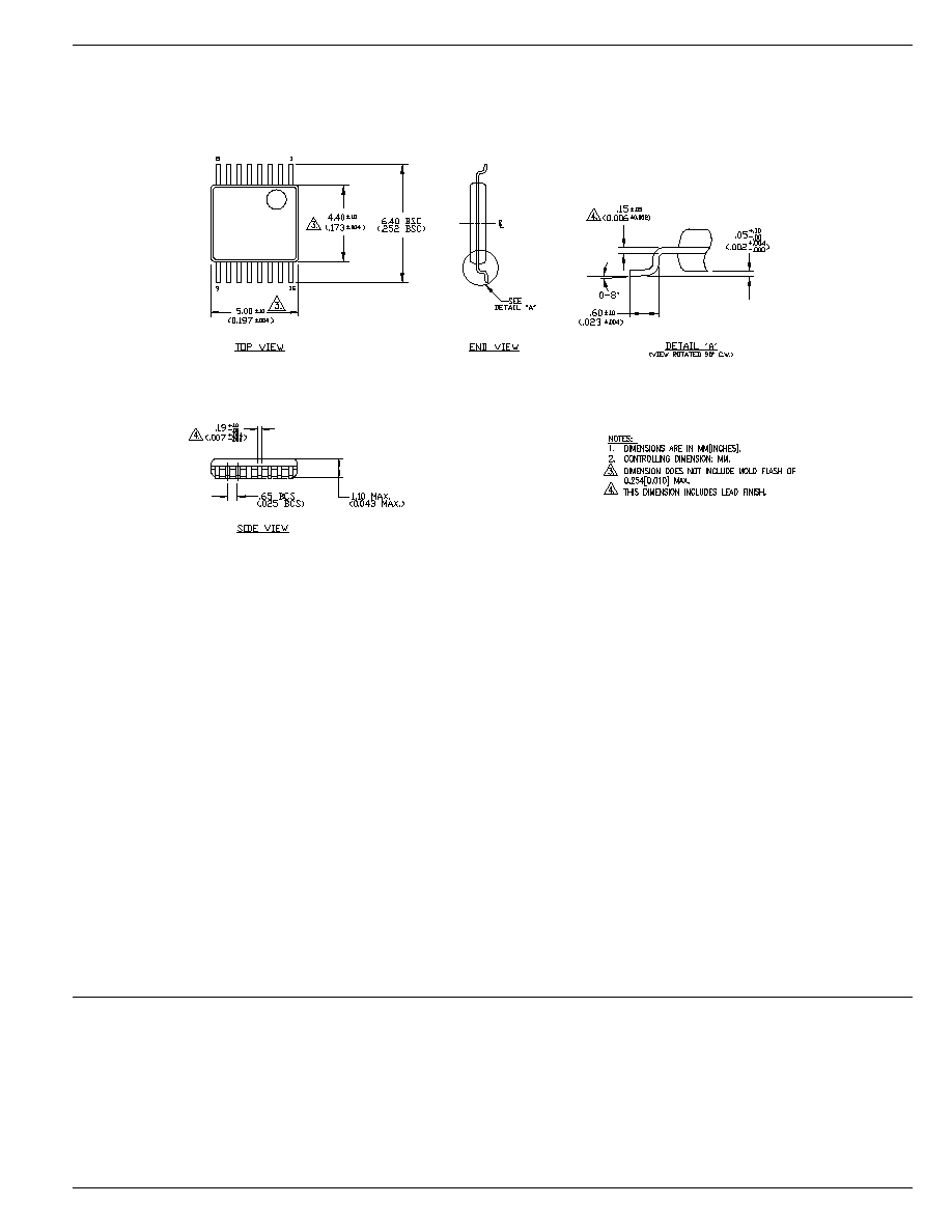
Package Information
Rev. 01
16-Pin TSSOP (TS)
MICREL, INC.
1849 FORTUNE DRIVE
SAN JOSE, CA 95131
USA
TEL
+ 1 (408) 944-0800
FAX
+ 1 (408) 944-0970
WEB
http://www.micrel.com
The information furnished by Micrel in this datasheet is believed to be accurate and reliable. However, no responsibility is assumed by Micrel for its use.
Micrel reserves the right to change circuitry and specifications at any time without notification to the customer.
Micrel Products are not designed or authorized for use as components in life support appliances, devices or systems where malfunction of a product can
reasonably be expected to result in personal injury. Life support devices or systems are devices or systems that (a) are intended for surgical implant into
the body or (b) support or sustain life, and whose failure to perform can be reasonably expected to result in a significant injury to the user. A Purchaser's
use or sale of Micrel Products for use in life support appliances, devices or systems is at Purchaser's own risk and Purchaser agrees to fully indemnify
Micrel for any damages resulting from such use or sale.
© 2003 Micrel, Incorporated.