 | –≠–ª–µ–∫—Ç—Ä–æ–Ω–Ω—ã–π –∫–æ–º–ø–æ–Ω–µ–Ω—Ç: MIC2072 | –°–∫–∞—á–∞—Ç—å:  PDF PDF  ZIP ZIP |

September 2000
1
MIC2012/2072
MIC2012
Micrel
MIC2012/MIC2072
USB Power Controller
Advance Information
General Description
The MIC2012 is a dual channel USB power switch designed
to support the power distribution requirements for USB Wakeup
from the ACPI S3 state. The MIC2012 will directly switch its
two outputs between a 5V main supply and a 5V auxiliary
supply normally provided in ATX style power supplies.
The MIC2012 will adjust its current-limit threshold according
to the ACPI state it is in. In the normal active S0 state the
current-limit is set at 500mA minimum per channel satisfying
the USB continuous output current specification. In the S3
state the current-limit can be reduced to only 100mA per
channel to minimize the current that is supplied by the
auxiliary supply thereby ensuring that voltage regulation is
maintained even during fault conditions.
The MIC2012 provides make-before-break switching to en-
sure glitch-free transitions between the S3 and S0 states.
Each channel is also thermally isolated from the other so that
a fault in one channel does not effect the other. FAULT status
output signals are also provided indicating overcurrent and
thermal shutdown conditions.
The MIC2072 option latches the output off upon detecting an
overcurrent condition for more than 5ms minimum. The
output can be reset by either toggling the EN inputs of the
MIC2072-1, -2 or by removing the load. Latching the output
off provides a circuit breaker mode of operation which re-
duces power consumption during fault conditions.
Typical Application
MIC2012P
V
BUS
D+
D≠
GND
MAIN
AUX
OUT1
Downstream
USB
Port 1
100
µ
F
5V MAIN
ATX Power Supply
S3#
FAULT1#
FAULT2#
V
BUS
D+
D≠
GND
Downstream
USB
Port 2
OUT2
GND
5V STANDBY
82801AA or Equivalent
SLP S3#
SLP S5#
OC0
OC1
Overcurrent Port 1
S3 Control
Overcurrent Port 1
100
µ
F
Figure 1. USB Wakeup with Control Input
Features
∑ Compliant to USB power distribution specifications
∑ Two completely independent switches
∑ Integrated switching matrix supports ACPI S0/S3 state
transitions without external FET circuits
∑ Make-before-break switching ensures glitch-free
transitions
∑ No back-feed of auxiliary supply onto main supply
during standby mode
∑ Bi-level current-limit preserves auxiliary supply voltage
regulation in standby mode
∑ Thermally isolated channels
∑ Thermal shutdown protection
∑ Fault status outputs with filter prevents false assertions
during hot-plug events
∑ Latched thermal shutdown options with auto-reset
(MIC2072)
∑ Undervoltage lockout
Applications
∑ Desktop PCs
∑ Notebook PCs
∑ Notebook Docking stations
∑ LAN Servers
∑ PC Motherboards
Micrel, Inc. ∑ 1849 Fortune Drive ∑ San Jose, CA 95131 ∑ USA ∑ tel + 1 (408) 944-0800 ∑ fax + 1 (408) 944-0970 ∑ http://www.micrel.com

MIC2012
Micrel
MIC2012/2072
2
September 2000
Pin Configuration
1
FAULT1
S3#
AUX
GND
8
FAULT2
OUT1
MAIN
OUT2
7
6
5
2
3
4
8-Pin SOIC (M)
Ordering Information
Fault
Circuit Breaker
Temperature
Part Number
Enable
Output
Function
Range
Package
MIC2012CM
n/a
Open-Drain
0
∞
C to +70
∞
C
8-lead SOIC
MIC2012PCM*
n/a
Internal Pull-Up
0
∞
C to +70
∞
C
8-lead SOIC
MIC2012-1CQS*
Active High
Open-Drain
0
∞
C to +70
∞
C
16-lead QSOP
MIC2012-1PCQS*
Active High
Internal Pull-Up
0
∞
C to +70
∞
C
16-lead QSOP
MIC2012-2CQS*
Active Low
Open-Drain
0
∞
C to +70
∞
C
16-lead QSOP
MIC2012-2PCQS*
Active Low
Internal Pull-Up
0
∞
C to +70
∞
C
16-lead QSOP
MIC2072CM*
n/a
Open-Drain
0
∞
C to +70
∞
C
8-lead SOIC
MIC2072PCM*
n/a
Internal Pull-Up
0
∞
C to +70
∞
C
8-lead SOIC
MIC2072-1CQS*
Active High
Open-Drain
0
∞
C to +70
∞
C
16-lead QSOP
MIC2072-1PCQS*
Active High
Internal Pull-Up
0
∞
C to +70
∞
C
16-lead QSOP
MIC2072-2CQS
Active Low
Open-Drain
0
∞
C to +70
∞
C
16-lead QSOP
MIC2072-2PCQS*
Active Low
Internal Pull-Up
0
∞
C to +70
∞
C
16-lead QSOP
* Contact factory for availability.
1
FAULT1
EN1
S3#
NC
AUX
NC
NC
GND
16 FAULT2
EN2
OUT1
OUT1
MAIN
MAIN
OUT2
OUT2
15
14
13
12
11
10
9
2
3
4
5
6
7
8
16-Pin QSOP (QS)

September 2000
3
MIC2012/2072
MIC2012
Micrel
Pin Description
Pin Number
Pin Number
Pin Name
Pin Function
(MIC2012)
(MIC2012-1, -2)
1
1
FAULT1
Fault Status (Output): Internal pull-up or open-drain. Asserted LOW when
Channel is in a thermal shutdown state or overcurrent condition for more
than 5ms. MIC2072 latches this output in its asserted state upon an
overcurrent condition. Toggling EN1 or removing the load will reset the
circuit breaker latch and deassert FAULT1.
n/a
2
EN1
Enable (Input): Channel 1, active-high (≠1) or active-low (≠2). Toggling this
input also resets the latched output of the MIC2072.
2
3
S3#
Control (Input): When this input is HIGH, the MAIN inputs are connected to
OUT1 and OUT2 via 100m
MOSFET switches. When this input is LOW the
AUX inputs are connected to OUT1 and OUT2 via 500m
MOSFET
switches.
3
5
AUX
Auxiliary 5V Supply (Input): Also used as power supply for internal circuitry.
n/a
4, 6, 7
NC
No Connection: This pin may be connected to other pins without restriction.
4
8
GND
Ground
5
9, 10
OUT2
Channel 2 (Output): For MIC2012-1, -2 both pins must be externally
connected together.
6
11, 12
MAIN
5V Main Supply (Input): All MAIN inputs must be connected together
externally.
7
13, 14
OUT1
Channel 1 (Output): For MIC2012-1, -2 both pins must be externally
connected together.
n/a
15
EN2
Enable (Input): Channel 2, active-high (≠1) or active-low (≠2). Toggling this
input also resets the latched output of the MIC2072.
8
16
FAULT2
Fault Status (Output): Internal pull-up or open-drain. Asserted LOW when
Channel 2 is in a thermal shutdown state or overcurrent condition for more
than 5ms. MIC2072 latches this output in its asserted state upon an
overcurrent condition. Toggling EN2 or removing the load will reset the
circuit breaker latch and deassert FAULT2.

MIC2012
Micrel
MIC2012/2072
4
September 2000
Absolute Maximum Ratings
(Note 1, Note 4)
Supply Voltage (V
IN,
V
MAIN,
V
AUX
) ................... ≠0.3V to 6V
EN1, EN2, S3# Input Pins ................................ ≠0.3V to 6V
FAULT#, OUT1, OUT2 Output Pins ................. ≠0.3V to 6V
FAULT Output Current ............................................... 25mA
ESD Rating, Note 3 ...................................................... 2kV
Operating Ratings
(Note 2)
Supply Voltage (V
MAIN,
V
AUX
) ..................... +4.5V to +5.5V
Ambient Temperature (T
A
) ........................... ≠0
∞
C to +70
∞
C
Junction Temperature (T
J
) ....................... Internally Limited
Package Thermal Resistance
QSOP
(
JA
) ....................................................... 163
∞
C/W
SOIC
(
JA
) ......................................................... 160
∞
C/W
Electrical Characteristics
V
MAIN
= 5V; AUX = 5V; T
A
= 25
∞
C; unless noted
Symbol
Parameter
Condition
Min
Typ
Max
Units
V
MAIN
MAIN Supply Voltage
4.5
5.0
5.5
V
I
MAIN (ON)
MAIN Supply Current Switches On
S3# = 1, no load
16
22
µ
A
Note 5
I
MAIN (OFF)
MAIN Supply Current Switches Off
S3# = 1, no load
5
µ
A
Note 5, (MIC20x2-1, MIC20x2-2 only)
I
LEAK
MAIN Reverse Leakage Current,
S3# = 0, both switches ON, V
MAIN
= 0V
≠10
+10
µ
A
V
AUX
AUX Supply Voltage
4.5
5.0
5.5
V
I
AUX ON
AUX Supply Current,
No load
.6
1
mA
both switches on, Note 5
S3# = 0
I
AUX OFF
AUX Supply Current, switches
No load
5
µ
A
off. (MIC20x2-1, MIC20x2-2 only)
S3# = 0
V
UV/AUX
AUX Undervoltage Lockout
V
AUX
increasing
3.5
3.7
4.0
V
Threshold
V
AUX
decreasing
3.3
3.5
3.8
V
V
HYS
AUX Undervoltage Lockout
200
mV
Hysteresis
R
DSMAIN
MAIN On-Resistance, Each Output
S3# = 1, I
OUT
= 500mA
100
140
m
R
DSAUX
AUX On-Resistance, Each Output
S3# = 0, I
OUT
= 100mA
500
700
m
I
LIMIT(MAIN)
MAIN Current-Limit Threshold
S3# = 1, V
OUT
= 4.0V, ramped load
0.5
1.25
A
MAIN Short-Circuit Current-Limit
V
OUT
= 0V
0.5
1.25
A
I
LIMIT(AUX)
AUXCurrent-Limit Threshold
S3# = 0, V
OUT
= 4.0V, ramped load
105
150
195
mA
AUX Short-Circuit Current-Limit
V
OUT
= 0V, C
OUT
= 100
µ
F
80
mA
V
TH
S3#, EN1, EN2. Input
High-to-Low transition
.8
1.5
V
Threshold Voltage
Low-to-High transition
1.7
2.0
V
(EN1, EN2, for MIC20x2-x only)
V
HYS
EN1, EN2 and S3# Input Hysteresis
200
mV
(EN1, EN2, for MIC20x2-x only)
I
IN
S3#, EN1, EN2 Input Current
V
S3/EN
= 5V, 0V
≠1
1
µ
A
(EN1, EN2, for MIC20x2-x only)
I
OFF
OUT1, OUT2 Leakage Current
Outputs are off, V
OUT
= 0
≠10
10
µ
A
(MIC2012-x, MIC2072-x only)
Pull-Up Current During Latched
Outputs latched off
1
mA
Output State (MIC2072-1, -2)

September 2000
5
MIC2012/2072
MIC2012
Micrel
Symbol
Parameter
Condition
Min
Typ
Max
Units
V
TH LATCH
Latch Reset Threshold
V
OUT
Rising
1.95
V
(MIC2072, MIC2072-x only)
Minimum Output Slew Rate
.4
V/s
to Reset Latch
(MIC2072, MIC2072-x only), Note 6
Overtemperature Threshold
T
J
increasing, single channel
140
∞
C
T
J
decreasing, single channel
120
∞
C
T
J
increasing, both channels
160
∞
C
T
J
decreasing, both channels
150
∞
C
V
OL
FAULT Output Low Voltage
I
FAULT
= 5mA
0.2
V
V
OH
FAULT Output High Voltage
I
FAULT
= ≠20
µ
A
4
V
(MIC2012-1P,-2P),(MIC2072-1P,-2P)
FAULT Output Off Current
V
FAULT
= 5V
.2
10
µ
A
(Not Applicable to 'P' Options)
T
H
MAIN to S3# Hold Time, Note 6
Figure 5
5
ms
T
S
MAIN to S3# Set-up Time, Note 6
Figure 5
0
ms
t
DLY
FAULT Delay Filter Response Time
Output shorted to ground, Figure 4
5
10
20
ms
(Overcurrent only), Note 7
t
OC
Overcurrent Response Time
Output shorted to ground, Figure 4
MAIN output
2
µ
s
AUX output
2
µ
s
t
ON(MAIN)
MAIN Output Turn-On Time
R
L
= 10
, C
L
= 1
µ
F, Figure 3
2
ms
t
OFF(MAIN)
MAIN Output Turn-Off Time
R
L
= 10
, C
L
= 1
µ
F, Figure 3
35
µ
s
(MIC20x2-x only)
t
r(MAIN)
MAIN Output Rise Time
R
L
= 10
, C
L
= 1
µ
F, Figure 3
2
ms
t
f(MAIN)
MAIN Output Fall Time
R
L
= 10
, C
L
= 1
µ
F, Figure 3
32
µ
s
(MIC20x2-x only)
t
ON(AUX)
AUX Output Turn-On Time
R
L
= 50
, C
L
= 1
µ
F, Figure 3
0.6
ms
t
OFF(AUX)
AUX Output Turn-Off Time
R
L
= 50
, C
L
= 1
µ
F, Figure 3
120
µ
s
(MIC20x2-x only)
t
r(AUX)
AUX Output Rise Time
R
L
= 50
, C
L
= 1
µ
F, Figure 3
0.5
ms
t
f(AUX)
AUX Output Fall Time
R
L
= 50
, C
L
= 1
µ
F, Figure 3
115
µ
s
(MIC20x2-x only)
t
XMA
MAIN to AUX
S3# transition to 0
5
7.5
ms
Cross Conduction Time, Note 8
t
XAM
AUX to MAIN
S3# transition to 1
5
7.5
ms
Cross Conduction Time, Note 8
Note 1.
Exceeding the absolute maximum rating may damage the device.
Note 2.
The device is not guaranteed to function outside its operating rating.
Note 3.
Devices are ESD sensitive. Handling precautions recommended. Human body model, 1.5k in series with 100pF.
Note 4.
All voltages are referenced to ground.
Note 5.
For MIC20x2-1(P) OFF occurs when V
EN
< 0.8V and ON occurs when V
EN
> 2.4V. For MIC20x2-2(P) OFF occurs when V
EN
> 2.4V and ON
occurs when V
EN
< 0.8V.
Note 6.
Guaranteed by design. Not production tested.
Note 7.
Assumes only one channel in current-limit. Delay circuitry is shared among channels so it is possible for t
DLY
to be 40ms max if one channel
enters current-limit as the other is about to time-out.
Note 8.
Cross conduction time is the duration in which both MAIN and AUX internal switches are on subsequent to S3# transitioning.

MIC2012
Micrel
MIC2012/2072
6
September 2000
Test Circuit
Device
Under
Test
C
L
OUT
R
L
V
OUT
I
OUT
90%
V
OUT
10%
90%
10%
t
r
t
f
September 2000
7
MIC2012/2072
MIC2012
Micrel
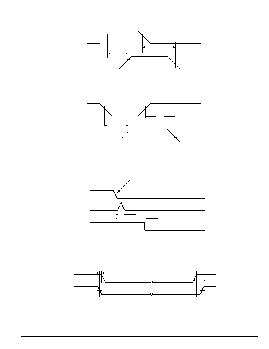
Timing Diagrams
V
EN
50%
90%
V
OUT
10%
t
OFF
t
ON
Figure 2. MIC2012/72-1
V
EN
50%
90%
V
OUT
10%
t
OFF
t
ON
Figure 3. MIC2012/72-2
Output shorted to ground
V
OUT
FAULT#
I
LIMIT
t
OC
t
DLY
I
OUT
Figure 4. Overcurrent Response Timing
MAIN
t
H
S3#
1.5V
t
S
1.5V
Figure 5. MAIN to S3# Timing
MIC2012
Micrel
MIC2012/2072
8
September 2000
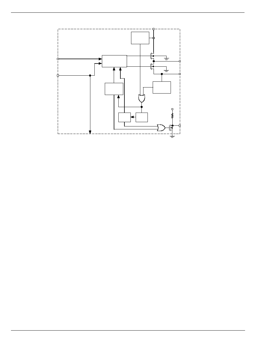
Functional Description
The MIC2012/2072 are designed to support the power distri-
bution requirements for USB wakeup from the ACPI S3 state.
It integrates two independent channels under control of input
S3#. When S3# is asserted LOW (S3 state) the MIC2012/
2072 will switch a 500m
, 100mA MOSFET switch from the
AUX input to each of its two outputs. Conversely when the
S3# input is HIGH (S0 state) the MIC2012/72 will switch a
100m
, 500mA MOSFET switch from the MAIN input to each
of its two outputs. The lower current limit during the ACPI S3
state helps to ensure that the standby supply maintains
regulation even during fault conditions.
Thermal Shutdown
Thermal shutdown is employed to protect the device from
damage should the die temperature exceed safe margins
due mainly to short circuit faults. Thermal shutdown shuts off
the output MOSFET and asserts the FAULT output if the die
temperature reaches 140
∞
C and the overheated channel is in
current limit. The other channel is not affected. If, however,
the die temperature exceeds 160
∞
C, both channels will be
shut off even if neither channel is in current limit.
Power Dissipation
The device's junction temperature depends on several fac-
tors such as the load, PCB layout, ambient temperature and
package type. The power dissipated in each channel is
P
D
= R
DS(on)
◊
I
OUT
2
where R
DS(on)
is the on-resistance of the
internal MOSFETs and I
OUT
is the continuous output current.
Total power dissipation of the device will be the summation of
P
D
for both channels. To relate this to junction temperature,
the following equation can be used:
TJ = P
D
◊
JA
+ T
A
where:
Functional Diagram
Current
Limit
10ms
Timer
Charge Pump
+
Gate Control
S3#
EN
Current
Limit
MAIN
OUT
AUX
/FAULT
AUX
Latch
To Other Channel
*
MAIN
FET
AUX
FET
*MIC2070-1/2 Only
Thermal
Sense
* 'P' options only
T
J
= junction temperature
T
A
= ambient temperature
JA
= is the thermal resistance of the package
Current Sensing and Limiting
The current-limit thresholds are preset internally for each
state. The preset level prevents damage to the device and
external load but still allows a minimum current of 100mA or
500mA to be delivered to the load depending on the state of
the device according to the S3# input. When S3# is LOW the
current-limit is set at 100mA minimum. When S3# is HIGH the
current-limit is set at 500mA minimum.
Should an over-current condition last longer than t
DLY
, the
MIC2072 will latch the faulty output off. The output will remain
off until either the load is removed or the EN signal (MIC2072-
1, -2) is toggled. When the MIC2072 enters a latched output
condition a 1mA pull-up current source is activated. This
provides a way to automatically reset the output once the load
is removed without the need to toggle the enable input such
as in the MIC2072. Please refer to Figure 7 for timing details.
The MIC2012 will automatically reset its output when the die
temperature cools down to 120
∞
C. The MIC2012 output and
FAULT signal will continue to cycle on and off until the device
is disabled or the fault is removed. Figure 6 depicts typical
timing. Depending on PCB layout, package, ambient tem-
perature, etc., it may take several hundred milliseconds from
the incidence of the fault to the output MOSFET being shut
off. This time duration will be shortest in the case of a dead
short on the output.

September 2000
9
MIC2012/2072
MIC2012
Micrel
Fault Status Output
The FAULT signal is an active-low output with an open-drain
or weak pull-up configuration. FAULT is asserted (active-low)
when either an overcurrent or thermal shutdown condition
occurs. In the case of an overcurrent condition, FAULT will be
asserted only after the flag response delay time, t
DLY
, has
elapsed. This ensures that FAULT is asserted only upon valid
overcurrent conditions and that erroneous error reporting is
eliminated. For example, false overcurrent conditions can
occur during hot-plug events when a highly capacitive load is
connected and causes a high transient inrush current that
exceeds the current-limit threshold. The FAULT response
delay time t
DLY
is typically 10ms.
Undervoltage Lockout
Undervoltage lockout (UVLO) prevents the output MOSFET
from turning on until the AUX input exceeds approximately
3.5V. UVLO ensures that the output MOSFETs remain off to
prevent high transient inrush current due to stray or bulk load
capacitance. This helps to ensure that the power supply
voltage regulation is preserved and also prevents possible
damage to sensitive components.
EN
(MIC2010-2)
V
OUT
Overcurrent Fault
Thermal Shutdown
Reached
FAULT
Figure 6. MIC2012 System Timing
EN
(MIC2070-2)
V
OUT
Overcurrent Fault
Load Removed≠
Output Reset
FAULT
Figure 7. MIC2072 System Timing--
Output Resets When Load is Removed
MIC2012
Micrel
MIC2012/2072
10
September 2000
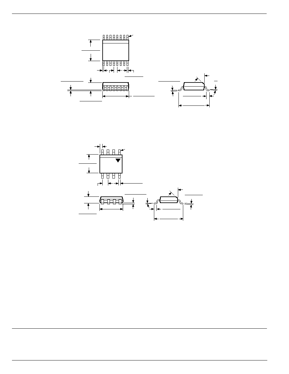
Package Information
45
∞
0.2284 (5.801)
0.2240 (5.690)
SEATING
PLANE
0.009 (0.2286)
REF
0.012 (0.30)
0.008 (0.20)
0.157 (3.99)
0.150 (3.81)
0.050 (1.27)
0.016 (0.40)
0.0688 (1.748)
0.0532 (1.351)
0.196 (4.98)
0.189 (4.80)
0.025 (0.635)
BSC
PIN 1
DIMENSIONS:
INCHES (MM)
0.0098 (0.249)
0.0040 (0.102)
0.0098 (0.249)
0.0075 (0.190)
8
∞
0
∞
16-Pin QSOP (QS)
45
∞
0
∞
≠8
∞
0.244 (6.20)
0.228 (5.79)
0.197 (5.0)
0.189 (4.8)
SEATING
PLANE
0.026 (0.65)
MAX
)
0.010 (0.25)
0.007 (0.18)
0.064 (1.63)
0.045 (1.14)
0.0098 (0.249)
0.0040 (0.102)
0.020 (0.51)
0.013 (0.33)
0.157 (3.99)
0.150 (3.81)
0.050 (1.27)
TYP
PIN 1
DIMENSIONS:
INCHES (MM)
0.050 (1.27)
0.016 (0.40)
8-Pin SOIC (M)
MICREL INC.
1849 FORTUNE DRIVE
SAN JOSE, CA 95131
USA
TEL
+ 1 (408) 944-0800
FAX
+ 1 (408) 944-0970
WEB
http://www.micrel.com
This information is believed to be accurate and reliable, however no responsibility is assumed by Micrel for its use nor for any infringement of patents or
other rights of third parties resulting from its use. No license is granted by implication or otherwise under any patent or patent right of Micrel Inc.
© 2000 Micrel Incorporated