
June 2000
1
MIC2141
MIC2141
Micrel
Micrel, Inc. ∑ 1849 Fortune Drive ∑ San Jose, CA 95131 ∑ USA ∑ tel + 1 (408) 944-0800 ∑ fax + 1 (408) 944-0970 ∑ http://www.micrel.com
MIC2141
Micropower Boost Converter
Preliminary Information
General Description
The MIC2141 is a micropower boost switching regulator that
can operate from 3- or 4-cell nickel-metal-hydride batteries or
a single Li-ion cell. This regulator employs a constant 330kHz,
fixed 18% duty-cycle, gated-oscillator architecture.
The MIC2141 can be used in applications where the output
voltage must be dynamically adjusted. The device features a
control signal input which is used to proportionally adjust the
output voltage. The control signal input has a gain of 6,
allowing a 0.8V to 3.6V control signal to vary a 4.8V to 22V
output.
The MIC2141 requires only three external components to
operate and is available in a tiny 5-lead SOT-23 package for
space and power-sensitive portable applications. The
MIC2141 draws only 70
µ
A of quiescent current and can
operate with an efficiency exceeding 85%.
Features
∑ Implements low-power boost, SEPIC, or flyback
∑ 2.5V to 14V input voltage
∑ 330kHz switching frequency
∑ <2
µ
A shutdown current
∑ 70
µ
A quiescent current
∑ 1.24V bandgap reference
∑ typical output current 1mA to 10mA
∑ SOT-23-5 Package
Applications
∑ LCD bias supply
∑ CCD digital camera supply
Ordering Information
Part Number
Junction Temp. Range
Package
MIC2141-BM5
≠40
∞
C to +85
∞
C
SOT-23-5
Typical Application
MIC2141
Variable
V
OUT
V
C
*
(from DAC)
10
µ
F
10
µ
H
1
5
2
3
4
0
0.5
1.0
1.5
2.0
2.5
3.0
3.5
4.0
0
5
10
15
20
25
V
C
(V)
V
OUT
(V)
Control Voltage
vs. Output Voltage
DAC-Controlled LCD Bias Voltage Supply
MIC2141
Micrel
MIC2141
2
June 2000
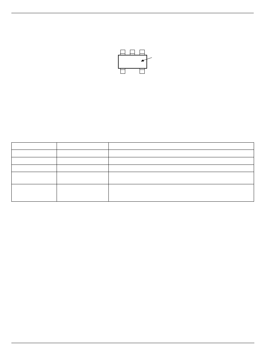
Pin Configuration
IN
VC
FB
SW
1
3
4
5
2
GND
Part
Identification
SAxx
SOT-23-5 (BM)
Pin Description
Pin Number
Pin Name
Pin Function
1
IN
Input: +2.5V to +14V supply for internal circuity.
2
GND
Ground: Return for internal circuitry and internal MOSFET (switch) source.
3
SW
Switch Node (Input): Internal MOSFET drain; 22V maximum.
4
FB
Feedback (Input): Output voltage sense node. Compared to V
C
control
input voltage.
5
VC
Control (Input): Output voltage control signal input. Input voltage of 0.8V to
3.6V is proportional to 4.8V to 22V output voltage (gain of 6). If the pin is not
connected, the output voltage will be V
IN
≠ 0.5V.

June 2000
3
MIC2141
MIC2141
Micrel
Absolute Maximum Ratings (Note 1)
Supply Voltage (V
IN
) ................................................... +18V
Switch Voltage (V
SW
) .................................................. +24V
Feedback Voltage (F
B
) ................................................ +24V
Control Input Voltage (V
C
), Note 3 .. V
IN
≠200mV
V
C
4V
ESD Rating, Note 4 ...................................................... 2kV
Operating Ratings (Note 2)
Supply Voltage (V
IN
) .................................... +2.5V to +14V
Switch Voltage (V
SW
) ...................................... +3V to +22V
Ambient Temperature (T
A
) ......................... ≠40
∞
C to +85
∞
C
Junction Tempgserature (T
J
) ................... ≠40
∞
C to +125
∞
C
Package Thermal Resistance
SOT-23-5 (
JA
) ...................................................... 220
∞
C/W
Electrical Characteristics
V
IN
= 3.6V, V
OUT
= 5V; I
OUT
= 1mA; T
J
= 25
∞
C, bold values indicate ≠40
∞
C
T
A
+85
∞
C; unless noted.
Parameter
Condition
Min
Typ
Max
Units
Input Voltage
2.5
14
V
Quiescent Current
Switch off, V
IN
= 3.6V
70
100
µ
A
Comparator Hysteresis
10
mV
Control Voltage Gain (V
OUT
/V
C
)
2.5V
V
IN
12V, V
OUT
= 15V
6
Controlled Output Voltage,
V
C
= 0.8V; 2.5V
V
IN
4.2V
4.85
5.0
5.15
V
Note 3
V
C
= 2.5V; 2.7V
V
IN
12V
14.55
15.0
15.45
V
V
C
= 3.4V; 3.6V
V
IN
12V
19.4
20.0
20.6
V
Load Regulation
100
µ
A
I
OUT
1mA, V
OUT
= 15V
0.25
1
%
Line Regulation
2.5V
V
IN
12V; I
OUT
1mA
0.05
0.2
%/V
Switch On-Resistance
I
SW
= 100mA, V
IN
= 3.6V
4
I
SW
= 100mA, V
IN
= 12V
2.5
Oscillator Frequency
300
330
360
kHz
Oscillator Duty Cycle
15
18
%
Note 1.
Exceeding the absolute maximum rating may damage the device.
Note 2.
The device is not guaranteed to function outside its operating rating.
Note 3.
V
C
= 4V sets V
OUT
to 24V (absolute maximum level on V
SW
); V
C
must be
V
IN
≠ 200mV.
Note 4.
Devices are ESD sensitive. Handling precautions recommended. Human body model, 1.5k in series with 100pF.

MIC2141
Micrel
MIC2141
4
June 2000
Typical Characteristcs
0
5
10
15
20
25
0
5
10
15
20
25
FEEDBACK CURRENT (
µ
A)
OUTPUT VOLTAGE (V)
Feedback Current
vs. Output Voltage
0
5
10
15
20
0
1
2
3
4
OUTPUT VOLTAGE (V)
CONTROL VOLTAGE (V)
Control Voltage
vs. Output Voltage
V
IN
= 5V
L = 33
µ
H
V
IN
= 3.6V
V
IN
= 2.5V
5.7
5.8
5.9
6.0
6.1
6.2
6.3
6.4
0
5
10
15
20
25
GAIN
OUTPUT VOLTAGE (V)
Gain
vs. Output Voltage
V
IN
= 5V
L = 33
µ
H
0
1
2
3
4
5
6
7
0
1
2
3
4
CONTROL CURRENT (nA)
CONTROL VOLTAGE (V)
Control Current
vs. Control Voltage
14.80
14.85
14.90
14.95
15.00
0
1
2
3
4
5
OUTPUT VOLTAGE (V)
LOAD CURRENT (mA)
Load Regulation
V
IN
= 5V
I
PEAK
= 100mA
L = 33
µ
H
I
PEAK
= 150mA
L = 22
µ
H
14.0
14.2
14.4
14.6
14.8
15.0
2
4
6
8
10
12
OUTPUT VOLTAGE (V)
INPUT VOLTAGE (V)
Line Regulation
L = 33
µ
H
I
L
= 100
µ
A
300
320
340
360
380
400
2
4
6
8
10
12
14
16
FREQUENCY (kHz)
INPUT VOLTAGE (V)
Oscillator Frequency
vs. Input Voltage
0
40
80
120
160
200
240
280
0
2
4
6
8
10 12 14 16
QUIESCENT CURRENT (
µ
A)
INPUT VOLTAGE (V)
Quiescent Current
vs. Input Voltage
0.50
0.52
0.54
0.56
0.58
0.60
-40 -20
0
20
40
60
80 100
ON-TIME (
µ
s)
TEMPERATURE (
∞
C)
On-Time
vs. Temperature
300
310
320
330
340
350
-40 -20
0
20
40
60
80 100
FREQUENCY (kHz)
TEMPERATURE (
∞
C)
Frequency
vs. Temperature
10
11
12
13
14
15
16
17
18
19
20
-40 -20
0
20
40
60
80 100
DUTY CYCLE (%)
TEMPERATURE (
∞
C)
Duty Cycle
vs. Temperature

June 2000
5
MIC2141
MIC2141
Micrel
14.00
14.20
14.40
14.60
14.80
15.00
-40 -20
0
20
40
60
80 100
OUTPUT VOLTAGE (V)
TEMPERATURE (
∞
C)
Output Voltage
vs. Temperature
V
IN
= 5V
L = 33
µ
H
0
10
20
30
40
50
60
70
80
90
2
4
6
8
10
12
RIPPLE VOLTAGE (mV)
INPUT VOLTAGE (V)
Ripple Voltage vs.
Input Voltage
V
OUT
= 15V
I
L
= 1mA
L = 100
µ
H
0
10
20
30
40
50
60
70
80
90
100
0
1
2
3
4
EFFICIENCY (%)
OUTPUT CURRENT (mA)
Efficiency
BAT54HT1 Diode
1N4148 Diode
V
IN
= 5V
V
OUT
= 15V
L = 33
µ
H
0
1
2
3
4
5
6
7
8
9
2
4
6
8
10
12
14
ON-RESISTANCE (
)
INPUT VOLTAGE (V)
On-Resistance vs.
Input Voltage
0
100
200
300
400
500
600
700
800
900
2
4
6
8
10
12
14
V
DS
(mV)
INPUT VOLTAGE (V)
Switch Voltage Drop
vs. Input Voltage
I
DS
= 100mA
0
1
2
3
4
5
6
7
8
-40 -20
0
20
40
60
80 100
R
DS(on)
(
)
TEMPERATURE (
∞
C)
Switch On-Resistance
vs. Temperature
V
IN
= 3.3V
0
100
200
300
400
500
600
700
800
-40 -20
0
20
40
60
80 100
V
DS
(mV)
TEMPERATURE (
∞
C)
Switch Voltage Drop
vs. Temperature
V
IN
= 3.3V
I
D
= 100mA
78
80
82
84
86
88
-40 -20
0
20
40
60
80 100
QUIESCENT CURRENT (
µ
A)
TEMPERATURE (
∞
C)
Quiescent Current
vs. Temperature
V
IN
= 5V
5.90
5.92
5.94
5.96
5.98
6.00
-40 -20
0
20
40
60
80 100
GAIN
TEMPERATURE (
∞
C)
Gain
vs. Temperature
V
IN
= 5V

MIC2141
Micrel
MIC2141
6
June 2000
Functional Diagram
330kHz
FIXED DUTY CYCLE
VC
FB
IN
GND
SW
Oscillator
MIC2141
Bandgap
Reference
Functional Description
See "Applications Information" for component selection and
predesigned circuits.
Overview
This MIC2141 is a fixed-duty-cycle, constant-frequency, gated-
oscillator, micropower, switch-mode power supply controller.
Quiescent current for the MIC2141 is only 70
µ
A in the switch
off state, and since a MOSFET output switch is used, addi-
tional current needed for switch drive is minimized. Efficien-
cies above 85% throughout most operating conditions can be
realized.
Regulaton
Regulation is performed by a hysteretic comparator which
regulates the output voltage by gating the internal oscillator.
The user applies a programming voltage to the VC pin. (For
a fixed or adjustable output regulator, with an internal refer-
ence, use the MIC2142.) The output voltage is divided down
internally and then compared to the V
C
, the control input
voltage, forcing the output voltage to 6 times the V
C
. The
comparator has hysteresis built into it, which determines the
amount of low frequency ripple that will be present on the
output. Once the feedback input to the comparator exceeds
the control voltage by 10mV, the high-frequency oscillator
drive is removed from the output switch. As the feedback
input to the comparator returns to the control voltage level,
the comparator is reset and the high-frequency oscillator is
again gated to the output switch. Typically 10mV of hysteresis
seen at the comparator will correspond to 60mV of low-
frequency ripple at the output. Applications, which require
continuous adjustment of the output voltage, can do so by
adjustment of the VC control pin.
Output
The maximum output voltage is limited by the voltage capa-
bility of the output switch. Output voltages up to 22V can be
achieved with a standard boost circuit. Higher output volt-
ages require a flyback configuration.
Output Voltage Control
The internal hysteretic comparator disables the output drive
once the output voltage exceeds the nominal by 30mV. The
drive is then enabled once the output voltage drops below the
nominal by 30mV.
The reference level, which actually programs the output
voltage, is set by the VC control input. The output is 6 times
the control voltage (V
C
) and the output ripple will be 6 times
the comparator hystersis. Therefore, with 10mV of hystersis,
there will be
±
30mV variation in the output around the nominal
value. See the "Typical Characteristics: Control Voltage vs.
Output Voltage" for a graph of input-to-output behavior.
The common-mode range of the comparator requires that the
maximum control voltage (V
C
) be held to 200mV less than
VIN. When programming for a 20V output, a minimum V
IN
of
3.5V will be required. See the "Typical Characteristics: Gain
vs. Output Voltage" for a graph of gain behavior. To achieve
20V output at lower input voltages, the external resistive
divider (R1 and R2) shown in Figure 2 can be added. This
circuit will increase the control-to-output gain, while limiting
the error introduced by the tolerance of the internal resistor
feedback network.

June 2000
7
MIC2141
MIC2141
Micrel
Application Information
Predesigned circuit information is at the end of this section.
Component Selection
Boost Inductor
Maximum power is delivered to the load when the oscillator
is gated
on 100% of the time. Total output power and circuit
efficiency must be considered when determining the maxi-
mum inductor. The largest inductor possible is preferable in
order to minimize the peak current and output ripple. Effi-
ciency can vary from 80% to 90% depending upon input
voltage, output voltage, load current, inductor, and output
diode.
Equation 1 solves for the output current capability for a given
inductor value and expected efficiency. Figures 5 through 9
graph estimates for maximum output current, assuming the
minimum duty cycle, maximum frequency, and 85% effi-
ciency. To determine the required inductance, find the inter-
section between the output voltage and current and select the
value of the inductor curve just above the intersection. If the
efficiency is expected to be other than the 85% used for the
graph, Equation 1 can then be used to better determine the
maximum output capability.
(1)
I
V
t
2L
T
V
eff
V
O(max)
IN(min) ON
MAX
S
O
IN min
=
(
)
◊
-
( )
2
1
The peak inductor and switch current can be calculated from
Equation 2 or read from the graph in Figure 10. The peak
current shown in Figure 10 is derived assuming a maximum
duty cycle and a minimum frequency. The selected inductor
and diode peak current capability must exceed this value.
The peak current seen by the inductor is calculated at the
maximum input voltage. A wider input voltage range will result
in a higher worst-case peak current in the inductor. This effect
can be seen in Table 4 by comparing the difference between
the peak current at V
IN(min)
and V
IN(max)
.
(2)
I
t
V
L
PK
ON max
IN max
MIN
=
(
)
(
)
DCM/CCM Boundary
Equation 3 solves for the point at which the inductor current
will transition from DCM (discontinuous conduction mode) to
CCM (continuous conduction mode). As the input voltage is
raised above this level the inductor has a potential for
developing a dc component while the oscillator is gated on.
Table 1 display the input points at which the inductor current
can possibly operate in the CCM region. Operation in this
region can result in a peak current slightly higher than
displayed Table 4.
(3)
V
V
V
1 D
IN ccm
OUT
FWD
(
)
=
+
(
)
+ -
(
)
Table 2 lists common inductors suitable for most applica-
tions. Table 6 lists minimum inductor sizes versus input and
output voltage. In low-cost, low-peak-current applications,
RF-type leaded inductors may sufficient. All inductors listed
in Table 4 can be found within the selection of CR32- or
LQH4C-series inductors from either Sumida or muRata.
r
e
r
u
t
c
a
f
u
n
a
M
s
e
i
r
e
S
e
p
y
T
e
c
i
v
e
D
a
t
a
R
u
m
C
4
/
C
3
/
C
1
H
Q
L
t
n
u
o
m
e
c
a
f
r
u
s
a
d
i
m
u
S
2
3
R
C
t
n
u
o
m
e
c
a
f
r
u
s
r
e
ll
i
M
.
W
.
J
F
8
7
d
e
d
a
e
l
l
a
i
x
a
t
f
a
r
c
li
o
C
0
9
d
e
d
a
e
l
l
a
i
x
a
Table 2. Inductor Examples
Boost Output Diode
Speed, forward voltage, and reverse current are very impor-
tant in selecting the output diode. In the boost configuration,
the average diode current is the same as the average load
current. (The peak current is the same as the peak inductor
current and can be derived from Equation 2 or Figure 10.)
Care must be take to make sure that the peak current is
evaluated at the maximum input voltage.
e
d
o
i
D
5
7
C
∞
V
D
W
F
t
a
A
m
0
0
1
C
∞
5
2
V
D
W
F
t
a
A
m
0
0
1
m
o
o
R
.
p
m
e
T
e
g
a
k
a
e
L
V
5
1
t
a
C
∞
5
7
e
g
a
k
a
e
L
V
5
1
t
a
e
g
a
k
c
a
P
0
3
5
0
R
B
M
V
5
7
2
.
0
V
5
2
3
.
0
A
µ
5
.
2
A
µ
0
9
3
2
1
D
O
S
T
M
S
8
4
1
4
N
1
V
6
.
0
)
C
∞
5
7
1
(
V
5
9
.
0
A
n
5
2
)
V
0
2
(
A
µ
2
.
0
)
V
0
2
(
d
e
d
a
e
l
T
M
S
d
n
a
4
5
T
A
B
V
4
.
0
)
C
∞
5
8
(
V
5
4
.
0
A
n
0
1
)
V
5
2
(
A
µ
1
)
V
0
2
(
T
M
S
5
8
T
A
B
4
5
.
0
)
C
∞
5
8
(
V
6
5
.
0
A
µ
4
.
0
A
µ
2
)
C
5
∞
8
(
4
3
-
O
D
d
e
d
a
e
l
Table 3. Diode Examples
As can be seen in the "Typical Characteristics: Efficiency"
graph, the output diode type can have an effect on circuit
efficiency. The BAT54- and BAT85-series diodes are low-
current Shottky diodes available from On Semiconductor and
Phillips, respectively. They are suitable for peak repetitive
currents of 300mA or less with good reverse current charac-
teristics. For applications that are cost driven, the 1N4148, or
equivalent, will provide sufficient switching speed with greater
forward drop and reduced cost. Other acceptable diodes are
On Semiconductor's MBR0530 or Vishay's B0530, although
they can have reverse currents that exceed 1mA at very high
junction temperatures. Table 3 summarizes some typical
performance characteristics of various suitable diodes.
V
T
U
O
V
)
M
C
C
(
N
I
V
3
.
3
V
4
0
.
3
V
0
.
5
V
0
4
.
4
V
0
.
9
V
0
6
.
7
V
0
.
2
1
V
0
.
0
1
V
0
.
5
1
V
4
.
2
1
V
0
.
6
1
V
2
.
3
1
V
0
.
0
2
V
4
.
6
1
V
0
.
2
2
V
0
.
8
1
Table 1. DCM/CCM Boundary

MIC2141
Micrel
MIC2141
8
June 2000
Output Capacitor
If the availability of tantalum capacitors is limited, ceramic
capacitors and inexpensive electrolyics may be necessary.
Selection of the capacitor value will depend upon on the peak
inductor current and inductor size. MuRata offers the GRM
series with up to 10
µ
F at 25V, with a Y5V temperature
coefficient, in a 1210 surface-mount package. Low-cost
applications can use M-series leaded electrolytic capacitors
from Panasonic. In general, ceramic, electrolytic, or tantalum
values ranging from 10
µ
F to 47
µ
F can be used for the output
capacitor.
r
e
r
u
t
c
a
f
u
n
a
M
s
e
i
r
e
S
e
p
y
T
e
g
a
k
c
a
P
a
t
a
R
u
m
M
R
G
V
5
Y
c
i
m
a
r
e
c
t
n
u
o
m
e
c
a
f
r
u
s
y
a
h
s
i
V
4
9
5
m
u
l
a
t
n
a
t
t
n
u
o
m
e
c
a
f
r
u
s
c
i
n
o
s
a
n
a
P
s
e
i
r
e
s
-
M
c
i
t
y
l
o
r
t
c
e
l
e
d
e
d
a
e
l
Table 4. Capacitor Examples
Design Example
Given a design requirement of 12V output and 1mA load with
a minimum input voltage of 2.5V, Equation 1 can be used to
calculate to maximum inductance or it can be read from the
graph in Figure 4. Once the maximum inductance has been
determined, the peak current can be determined using Equa-
tion 2 or Figure 10.
V
OUT
= 12V
I
OUT
= 1mA
V
IN
= 4.8V to 2.5V
SW
GND
FB
IN
VC
1
5
3
2
4
MIC2141
C4
0.1
µ
F
C1
10
µ
F
25V
CR1
BAT54HT1
L1
33
µ
H
C2
10
µ
F
25V
V
OUT
+5V to +15V
Return
V
IN
+2.7V to +12V
V
C
Return
Figure 1. Basic Configuration
SW
GND
FB
IN
VC
4
5
3
1
2
MIC2141
C4
0.1
µ
F
R1
34.8k
R2
121k
C1
10
µ
F
25V
CR1
BAT54HT1
L1
22
µ
H
C2
10
µ
F
25V
V
OUT
+5V to +20V
I
FB
Return
V
IN
+2.7V to +12V
V
C
Return
V
6V
1
R1
R2
I
R1
I
15 A for V
15V
OUT
C
FB
FB(typ)
OUT
==
++
++
==
==
µ
Figure 2. Gain-Boost Configuration
SW
GND
FB
IN
VC
1
5
3
2
4
MIC2141
C4
0.1
µ
F
C1
10
µ
F
25V
CR1
MBR0530
CR3
1N4148
CR2
1N4148
L1
4.7
µ
H
C2
10
µ
F
25V
V
OUT
+12V
Return
V
IN
+2.7V to +4.7V
V
C
Return
Figure 3. Bootstrap Configuration
L
V
t
I
V
eff
V
2
L
17 H
MAX
IN(min)
ON(min)
O(max)
O
IN(min)
MAX
==
--
==
2
2
T
S(min)
µ
Select 15
µ
H
±
10%.
I
t
V
L
0.767 s
4.8V
13.5 H
I
272mA
PEAK
ON(max)
IN(max)
MIN
PEAK
==
==
==
µ
µ
Select a BAT54 diode and CR32 inductor.
Always check the peak current to insure that it is within the
limits specified in the load line shown in Figure 10 for all
input and output voltages.
Gain Boost
Use Figure 2 to increase the voltage gain of the system. The
typical gain can easily be increased from the nominal gain of
6 to a value of 8 or 10. Figure 2 shows a gain of 8 so that with
2.5V applied to VC, V
OUT
will be 20V.
Bootstrap
The bootstrap configuration is used to increase the maximum
output current for a given input voltage. This is most effective
when the input voltage is less than 5V. Output current can
typically be tripled by using this technique. See Table 4a. for
bootstrap-ready-built component values.

June 2000
9
MIC2141
MIC2141
Micrel
Inductor Selection Guides
0.1
1
10
40
0
2
4
6
8
10
12
14
16
18
20
22
MAX. OUTPUT CURRENT (mA)
OUTPUT VOLTAGE (V)
3.9
µ
H
4.7
µ
H
18
µ
H
22
µ
H
15
µ
H
220
µ
H
180
µ
H
150
µ
H
120
µ
H
100
µ
H
82
µ
H
68
µ
H
56
µ
H
47
µ
H
39
µ
H
33
µ
H
27
µ
H
V
IN
= 2.5V
Figure 5. Inductor Selection for V
IN
= 2.5V
0.1
1
10
100
200
0
2
4
6
8
10
12
14
16
18
20
22
MAX. OUTPUT CURRENT (mA)
OUTPUT VOLTAGE (V)
12
µ
H
18
µ
H
22
µ
H
15
µ
H
220
µ
H
180
µ
H
150
µ
H
120
µ
H
100
µ
H
82
µ
H
68
µ
H
56
µ
H
47
µ
H
39
µ
H
33
µ
H
27
µ
H
4.7
µ
H
10
µ
H
V
IN
= 3.3V
Use for Li-ion battery
Figure 6. Inductor Selection for V
IN
= 3.3V

MIC2141
Micrel
MIC2141
10
June 2000
0.1
1
10
100
200
2
4
6
8
10
12
14
16
18
20
22
MAX. OUTPUT CURRENT (mA)
OUTPUT VOLTAGE (V)
12
µ
H
18
µ
H
22
µ
H
15
µ
H
220
µ
H
180
µ
H
150
µ
H
120
µ
H
100
µ
H
82
µ
H
68
µ
H
56
µ
H
47
µ
H
39
µ
H
33
µ
H
27
µ
H
8.2
µ
H
10
µ
H
V
IN
= 5V
Figure7. Inductor Selection for V
IN
= 5V
1
10
100
8
10
12
14
16
18
20
22
MAX. OUTPUT CURRENT (mA)
OUTPUT VOLTAGE (V)
18
µ
H
22
µ
H
15
µ
H
220
µ
H
180
µ
H
150
µ
H
120
µ
H
100
µ
H
82
µ
H
68
µ
H
56
µ
H
47
µ
H
39
µ
H
33
µ
H
27
µ
H
270
µ
H
330
µ
H
390
µ
H
470
µ
H
V
IN
= 9V
Figure 8. Inductor Selection for V
IN
= 9V

June 2000
11
MIC2141
MIC2141
Micrel
1
10
100
10
12
14
16
18
20
22
MAX. OUTPUT CURRENT (mA)
OUTPUT VOLTAGE (V)
22
µ
H
18
µ
H
220
µ
H
180
µ
H
150
µ
H
120
µ
H
100
µ
H
82
µ
H
68
µ
H
56
µ
H
47
µ
H
39
µ
H
33
µ
H
27
µ
H
270
µ
H
330
µ
H
390
µ
H
470
µ
H
V
IN
= 12V
Figure 9. Inductor Selection for V
IN
= 12V

MIC2141
Micrel
MIC2141
12
June 2000
0
100
200
300
400
500
600
700
800
900
1000
0
2
4
6
8
10
12
14
PEAK CURRENT (mA)
INPUT VOLTAGE (V)
12
µ
H
18
µ
H
22
µ
H
15
µ
H
220
µ
H
180
µ
H
150
µ
H
120
µ
H
100
µ
H
82
µ
H
68
µ
H
56
µ
H
47
µ
H
39
µ
H
33
µ
H
27
µ
H
8.2
µ
H
10
µ
H
270
µ
H
330
µ
H
390
µ
H
470
µ
H
3.9
µ
H
4.7
µ
H
Figure 10. Peak Inductor Current vs. Input Voltage

June 2000
13
MIC2141
MIC2141
Micrel
Predesigned Circuit Values
I
PEAK
I
PEAK
V
IN(min)
V
IN(max)
V
OUT
I
OUT(max)
L1
CR1
(V
IN
= V
OUT
≠ 0.5V) or 14V
(V
IN
= V
IN(min)
)
2.5V
4.5V
5.0V
4mA
15
µ
H
BAT54
230mA
128mA
3mA
18
µ
H
BAT54
192mA
106mA
2mA
27
µ
H
BAT54
128mA
71mA
1mA
56
µ
H
BAT54
62mA
34mA
0.5mA
120
µ
H
BAT54
29mA
16mA
5V bootstrap
14.8mA
3.9
µ
H
MBR0503
890mA
500mA
2.5V
11.5V
12V
1mA
15
µ
H
MBR0530
588mA
128mA
0.5mA
33
µ
H
BAT54
267mA
58mA
0.2mA
82
µ
H
BAT54
108mA
23mA
2.5V
4.7V
12V bootstrap
3.5mA
4.7
µ
H
MBR0503
750mA
500mA
2.5V
4.7V
12V bootstrap
4.3mA
3.9
µ
H
MBR0503
900mA
500mA
2.5V
14V
15V
0.8mA
15
µ
H
MBR0530
741mA
128mA
0.5mA
27
µ
H
MBR0530
412mA
71mA
0.2mA
68
µ
H
BAT54
163mA
28mA
2.5V
14V
16V
0.8mA
15
µ
H
MBR0530
710mA
128mA
0.5mA
22
µ
H
MBR0530
456mA
87mA
0.2mA
56
µ
H
BAT54
190mA
34mA
2.5V
14V
22V
0.5mA
15
µ
H
MBR0530
590mA
128mA
0.2mA
39
µ
H
BAT54
274mA
49mA
0.1mA
82
µ
H
BAT54
130mA
23mA
3.0V
4.5V
5V
10mA
12
µ
H
BAT54
288mA
190mA
use for Li-ion
3.6mA
27
µ
H
BAT54
128mA
85mA
battery range
0.8mA
120
µ
H
BAT54
29mA
19mA
5V bootstrap
20mA
4.7
µ
H
MBR0530
730mA
450mA
3.0V
8.5V
9V
3mA
12
µ
H
MBR0530
652mA
190mA
use for Li-ion
1.7mA
22
µ
H
MBR0530
296mA
103mA
battery range
0.8mA
47
µ
H
MBR0530
139mA
49mA
3.0V
4.7V
9V bootstrap
8mA
4.7
µ
H
MBR0503
750mA
450mA
use for Li-ion
battery range
3.0V
11.5V
12V
2.1mA
12
µ
H
MBR0530
882mA
190mA
use for Li-ion
1.7mA
15
µ
H
MBR0530
588mA
156mA
battery range
1mA
27
µ
H
MBR0530
327mA
85mA
0.45mA
56
µ
H
BAT54
157mA
40mA
3.0V
4.7V
12V bootstrap
5.4mA
4.7
µ
H
MBR0530
750mA
450mA
use for Li-ion
battery range
3.0V
14V
15V
1.6mA
12
µ
H
MBR0530
926mA
190mA
use for Li-ion
0.87mA
22
µ
H
MBR0530
505mA
103mA
battery range
0.41mA
47
µ
H
BAT54
237mA
49mA
3.0V
4.7V
15V bootstrap
4mA
4.7
µ
H
MBR0530
750mA
450mA
use for Li-ion
battery range
3.0V
14V
22V
1mA
10
µ
H
MBR0530
1071mA
190mA
use for Li-ion
0.8mA
15
µ
H
MBR0530
714mA
152mA
battery range
0.46mA
27
µ
H
MBR0530
400mA
85mA
0.2mA
68
µ
H
BAT54
157mA
3.3mA
Table 4a. Typical Configurations for Wide-Range Inputs--2.5V to 3.0V Minimum Input

MIC2141
Micrel
MIC2141
14
June 2000
I
PEAK
I
PEAK
V
IN(min)
V
IN(max)
V
OUT
I
OUT(max)
L1
CR1
(V
IN
= V
OUT
≠ 0.5V)
(V
IN
= V
IN(min)
)
5.0V
8.5V
9V
17mA
8.2
µ
H
MBR0530
795mA
467mA
15mA
10
µ
H
MBR0530
652mA
383mA
10mA
12
µ
H
MBR0530
643mA
319mA
5mA
27
µ
H
BAT54
241mA
142mA
1mA
120
µ
H
BAT54
54mA
32mA
5.0V
11.5V
12V
10mA
8.2
µ
H
MBR0530
1,075mA
467mA
5mA
18
µ
H
MBR0530
490mA
213mA
2mA
39
µ
H
BAT54
226mA
98mA
1mA
82
µ
H
BAT54
108mA
47mA
5.0V
14V
15V
7mA
8.2
µ
H
MBR0530
1356mA
467mA
5mA
12
µ
H
MBR0530
926mA
319mA
2mA
27
µ
H
MBR0530
412mA
142mA
1mA
56
µ
H
BAT54
199mA
68mA
5.0V
14V
16V
2.5mA
22
µ
H
MBR0530
986mA
174mA
1mA
56
µ
H
BAT54
190mA
68mA
0.5mA
120
µ
H
BAT54
90mA
32mA
5.0V
14V
22V
1.7mA
22
µ
H
MBR0530
486mA
174mA
1.0mA
39
µ
H
BAT54
274mA
98mA
0.5mA
82
µ
H
BAT54
130mA
47mA
0.1mA
180
µ
H
BAT54
60mA
21mA
9.0V
11.5V
12V
33mA
15
µ
H
MBR0530
588mA
460mA
20mA
22
µ
H
MBR0530
401mA
314mA
10mA
47
µ
H
BAT54
188mA
147mA
5mA
100
µ
H
BAT54
88mA
69mA
1mA
470
µ
H
BAT54
19mA
15mA
9.0V
14V
15V
20mA
15
µ
H
MBR0530
741mA
460mA
10mA
27
µ
H
MBR0530
412mA
256mA
5mA
56
µ
H
BAT54
199mA
123mA
2mA
150
µ
H
BAT54
74mA
46mA
1mA
270
µ
H
BAT54
41mA
26mA
9.0V
14V
20V
4.5mA
39
µ
H
BAT54
215mA
177mA
2mA
68
µ
H
BAT54
131mA
84mA
1mA
150
µ
H
BAT54
72mA
46mA
9.0V
14V
22V
4mA
39
µ
H
BAT54
275mA
177mA
2mA
68
µ
H
BAT54
157mA
101mA
1mA
150
µ
H
BAT54
72mA
46mA
12V
14V
15V
45mA
18
µ
H
MBR0530
618mA
511mA
20mA
39
µ
H
BAT54
285mA
236mA
10mA
82
µ
H
BAT54
136mA
112mA
5mA
150
µ
H
BAT54
74mA
61mA
1.7mA
470
µ
H
BAT54
24mA
20mA
12V
14V
20V
8mA
47
µ
H
BAT54
230mA
196mA
5mA
68
µ
H
BAT54
158mA
135mA
2mA
120
µ
H
BAT54
90mA
77mA
1mA
390
µ
H
BAT54
27mA
24mA
12V
21.5V
22V
7mA
47
µ
H
BAT54
228mA
196mA
5mA
68
µ
H
BAT54
157mA
135mA
2mA
150
µ
H
BAT54
69mA
61mA
1mA
220
µ
H
BAT54
47mA
42mA
Table 4b. Typical Configurations for Wide-Range Inputs--5V to 15V Minimum Input

June 2000
15
MIC2141
MIC2141
Micrel
I
PEAK
V
IN
V
OUT
I
OUT
L1
CR1
(typical)
3.3V
±
5%
5V
13mA
10
µ
H
BAT54
253mA
9V
5mA
10
µ
H
BAT54
253mA
12V
3mA
10
µ
H
BAT54
253mA
15V
2.3mA
10
µ
H
BAT54
253mA
20V
1.7mA
10
µ
H
BAT54
253mA
5V
±
5%
9V
17mA
8.2
µ
H
MB0530
467mA
12V
10.4mA
8.2
µ
H
MB0530
467mA
15V
7.5mA
8.2
µ
H
MB0530
467mA
20V
2.2mA
22
µ
H
MB0530
174mA
12V
±
5%
15V
44mA
18
µ
H
MB0530
511mA
20V
8.3mA
47
µ
H
BAT54
196mA
Table 5. Typical Maximum Power Configuration for Regulated Inputs
Output Voltage
V
IN
16V to 22V
4.5V to 15V
2.5V
15
µ
H
15
µ
H
3.0V
12
µ
H
12
µ
H
3.3V
10
µ
H
10
µ
H
3.5V
8.2
µ
H
8.2
µ
H
4.0V
27
µ
H
6.8
µ
H
4.5V
27
µ
H
6.8
µ
H
5.0V
22
µ
H
8.2
µ
H
6.0V
27
µ
H
10
µ
H
7.0V
27
µ
H
10
µ
H
8.0V
33
µ
H
12
µ
H
9.0V
39
µ
H
15
µ
H
10V
39
µ
H
15
µ
H
11V
47
µ
H
18
µ
H
12V
47
µ
H
18
µ
H
13V
56
µ
H
22
µ
H
14V
56
µ
H
22
µ
H
15V
56
µ
H
27
µ
H
16V
68
µ
H
27
µ
H
Table 6. Minimum Inductance
Manufacturer
Web Address
muRata
www.MuRata.com
Sumida
www.sumida.com
Coilcraft
www.coilcraft.com
J. W. Miller
www.jwmiller.com
Micrel
www.micrel.com
Vishay
www.vishay.com
Panasonic
www.panasonic.com
Table 7. Component Supplier Websites

MIC2141
Micrel
MIC2141
16
June 2000
Package Information
0.20 (0.008)
0.09 (0.004)
0.60 (0.024)
0.10 (0.004)
3.02 (0.119)
2.80 (0.110)
10
∞
0
∞
3.00 (0.118)
2.60 (0.102)
1.75 (0.069)
1.50 (0.059)
0.95 (0.037) REF
1.30 (0.051)
0.90 (0.035)
0.15 (0.006)
0.00 (0.000)
DIMENSIONS:
MM (INCH)
0.50 (0.020)
0.35 (0.014)
1.90 (0.075) REF
SOT-23-5 (M)
MICREL INC.
1849 FORTUNE DRIVE
SAN JOSE, CA 95131
USA
TEL
+ 1 (408) 944-0800
FAX
+ 1 (408) 944-0970
WEB
http://www.micrel.com
This information is believed to be accurate and reliable, however no responsibility is assumed by Micrel for its use nor for any infringement of patents or
other rights of third parties resulting from its use. No license is granted by implication or otherwise under any patent or patent right of Micrel Inc.
© 2000 Micrel Incorporated