 | –≠–ª–µ–∫—Ç—Ä–æ–Ω–Ω—ã–π –∫–æ–º–ø–æ–Ω–µ–Ω—Ç: MIC2172 | –°–∫–∞—á–∞—Ç—å:  PDF PDF  ZIP ZIP |

1997
4-13
MIC2172/3172
Micrel
4
slave's. The master MIC2172's oscillator frequency is in-
creased up to 135kHz by connecting a resistor from SYNC to
ground (see applications information).
The MIC2172/3172 is available in an 8-pin plastic DIP or
SOIC for ≠40
∞
C to +85
∞
C operation.
Features
∑ 1.25A, 65V internal switch rating
∑ 3V to 40V input voltage range
∑ Current-mode operation
∑ Internal cycle-by-cycle current limit
∑ Thermal shutdown
∑ Low external parts count
∑ Operates in most switching topologies
∑ 7mA quiescent current (operating)
∑ <1
µ
A quiescent current, shutdown mode (MIC3172)
∑ TTL shutdown compatibility (MIC3172)
∑ External frequency synchronization (MIC2172)
∑ External frequency trim (MIC2172)
∑ Fits most LT1172 sockets (see applications info)
Applications
∑ Laptop/palmtop computers
∑ Toys
∑ Hand-held instruments
∑ Off-line converter up to 50W
(requires external power switch)
∑ Predriver for higher power capability
∑ Master/slave configurations (MIC2172)
General Description
The MIC2172 and MIC3172 are complete 100kHz SMPS
current-mode controllers with internal 65V 1.25A power
switches. The MIC2172 features external frequency syn-
chronization or frequency adjustment, while the MIC3172
features an enable/shutdown control input.
Although primarily intended for voltage step-up applications,
the floating switch architecture of the MIC2172/3172 makes
it practical for step-down, inverting, and Cuk configurations
as well as isolated topologies.
Operating from 3V to 40V, the MIC2172/3172 draws only
7mA of quiescent current making it attractive for battery
operated supplies.
The MIC3172 is for applications that require on/off control of
the regulator. The MIC3172 is externally shutdown by
applying a TTL low signal to EN (enable). When disabled, the
MIC3172 draws only leakage current (typically less than
1
µ
A). EN must be high for normal operation. For applications
not requiring control, EN must be tied to V
IN
or TTL high.
The MIC2172 is for applications requiring two or more SMPS
regulators that operate from the same input supply. The
MIC2172 features a SYNC input which allows locking of its
internal oscillator to an external reference. This makes it
possible to avoid the audible beat frequencies that result from
the unequal oscillator frequencies of independent SMPS
regulators.
A reference signal can be supplied by one MIC2172 desig-
nated as a master. To insure locking of the slave's oscillators,
the reference oscillator frequency must be higher than the
MIC2172/3172
100kHz 1.25A Switching Regulators
Preliminary Information
Typical Applications
C4
470µF
D2
1N5818
C1
22µF
C2
1µF
R3
1k
R4*
V
OUT
5V, 0.25A
* Optional voltage clipper (may be req'd if T1 leakage inductance too high)
C3*
D1*
R1
3.74k
1%
R2
1.24k
1%
V
IN
4V to 6V
T1
Enable
Shutdown
1:1.25
L
PRI
= 100µH
MIC3172
V
IN
V
SW
FB
EN
GND
P1 P2 S
COMP
Figure 2.
MIC3172 5V Flyback Converter
+5V
(4.75V min.)
D1
1N5822
MIC2172
V
IN
V
SW
FB
C1*
22µF
R3
1k
C3
1µF
R1
10.7k
1%
C2
470µF
V
OUT
+12V, 0.14A
L1
27µH
* Locate near MIC2172 when supply leads > 2
"
R2
1.24k
1%
SYNC
GND
P1 P2 S
N/C
COMP
Figure 1.
MIC2172 5V to 12V Boost Converter

MIC2172/3172
Micrel
4-14
1997
Ordering Information
Part Number
Temperature Range
Package
MIC2172BN
≠40
∞
C to +85
∞
C
8-pin plastic DIP
MIC2172BM
≠40
∞
C to +85
∞
C
8-lead SOIC
MIC3172BN
≠40
∞
C to +85
∞
C
8-pin plastic DIP
MIC3172BM
≠40
∞
C to +85
∞
C
8-lead SOIC
8-lead SOIC (M)
8-lead DIP (N)
1
2
3
4
S GND
COMP
P GND 1
FB
*SYNC/
EN
V
SW
V
I N
P GND 2
8
7
6
5
MIC2172*/3172
Pin Configuration
1
2
3
4
S GND
COMP
P GND 1
FB
*SYNC/
EN
V
SW
V
I N
P GND 2
8
7
6
5
MIC2172*/3172
Pin Description
Pin Number
Pin Name
Pin Function
1
S GND
Signal Ground: Internal analog circuit ground. Connect directly to the input
filter capacitor for proper operation (see applications info). Keep separate
from power grounds.
2
COMP
Frequency Compensation: Output of transconductance type error amplifier.
Primary function is for loop stabilization. Can also be used for output voltage
soft-start and current limit tailoring.
3
FB
Feedback: Inverting input of error amplifier. Connect to external resistive
divider to set power supply output voltage.
4 (MIC2172)
SYNC
Synchronization/Frequency Adjust: Capacitively coupled input signal greater
than device's free running frequency (up to 135kHz) will lock device's
oscillator on falling edge. Oscillator frequency can be trimmed up to 135kHz
by adding a resistor to ground. If unused, pin must float (no connection).
4 (MIC3172)
EN
Enable: Apply TTL high or connect to V
IN
to enable the regulator. Apply
TTL low or connect to ground to disable the regulator. Device draws only
leakage current (<1
µ
A) when disabled.
5
V
IN
Supply Voltage: 3.0V to 40V
6
P GND 2
Power Ground #2: One of two NPN power switch emitters with 0.3
current
sense resistor in series. Required. Connect to external inductor or input
voltage ground depending on circuit topology.
7
V
SW
Power Switch Collector: Collector of NPN switch. Connect to external
inductor or input voltage depending on circuit topology.
8
P GND 1
Power Ground #1: One of two NPN power switch emitters with 0.3
current
sense resistor in series. Optional. For maximum power capability connect
to P GND 2. Floating pin reduces current limit by a factor of two.

1997
4-15
MIC2172/3172
Micrel
4
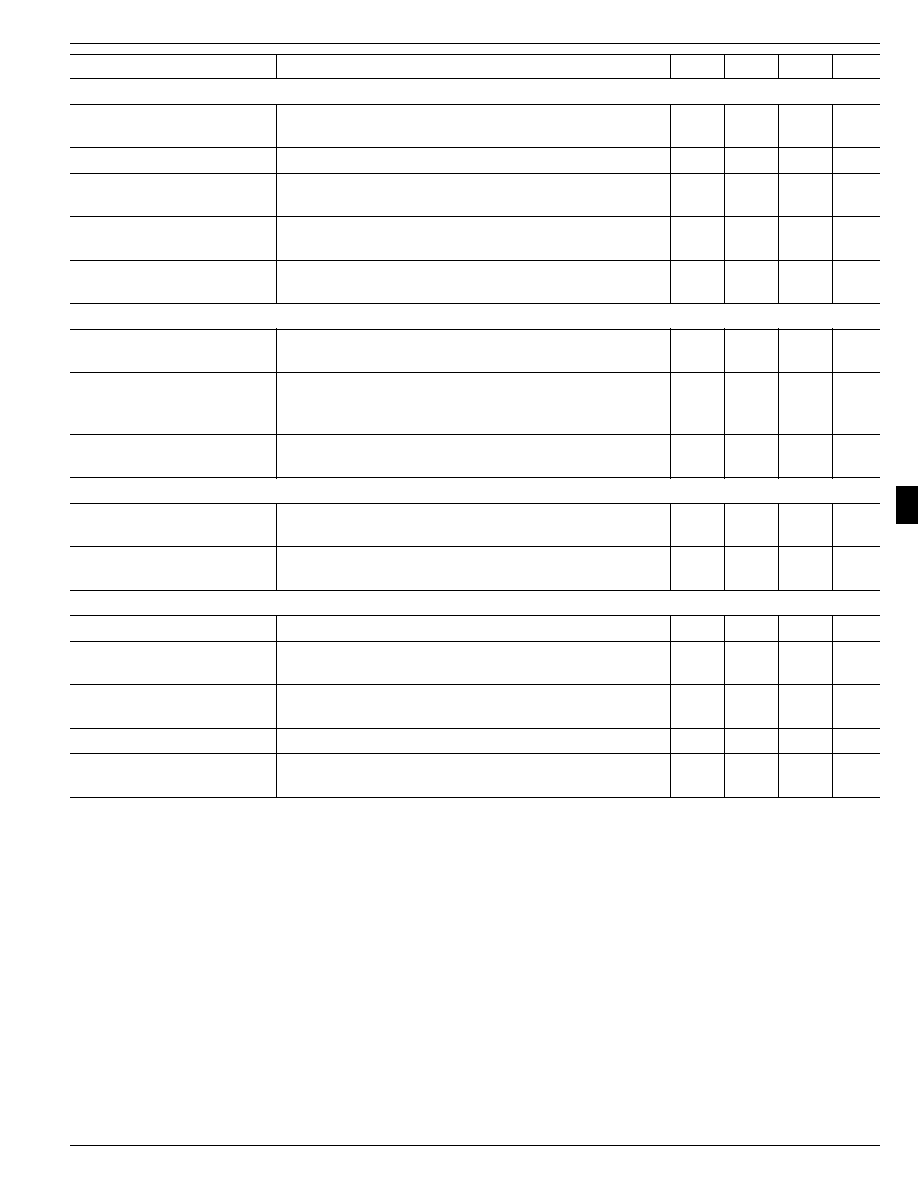
Electrical Characteristics MIC2172
Note 1. Unless otherwise specified, V
IN
= 5V.
Parameter
Conditions
Min
Typ
Max
Units
Reference Section
Pin 2 tied to pin 3
Feedback Voltage (V
FB
)
1.220
1.240
1.264
V
1.214
1.274
V
Feedback Voltage
3V
V
IN
40V
0.03
%/V
Line Regulation
Feedback Bias Current (I
FB
)
310
750
nA
1100
nA
Error Amplifier Section
Transconductance (
I
COMP
/
V
FB
)
I
COMP
=
±
25
µ
A
3.0
3.9
6.0
µ
A/mV
2.4
7.0
µ
A/mV
Voltage Gain (
V
COMP
/
V
FB
)
0.9V
V
COMP
1.4V
500
800
2000
V/V
Output Current
V
COMP
= 1.5V
125
175
350
µ
A
100
400
µ
A
Output Swing
High Clamp, V
FB
= 1V
1.8
2.1
2.3
V
Low Clamp, V
FB
= 1.5V
0.25
0.35
0.52
V
Compensation Pin
Duty Cycle = 0
0.8
0.9
1.08
V
Threshold
0.6
1.25
V
Output Switch Section
ON Resistance
I
SW
= 1A, V
FB
= 0.8V
0.76
1
1.1
Current Limit
Duty Cycle = 50%, T
J
25
∞
C
1.25
3
A
Duty Cycle = 50%, T
J
< 25
∞
C
1.25
3.5
A
Duty Cycle = 80% Note 2
1
2.5
A
Breakdown Voltage (BV)
3V
V
IN
40V
65
75
V
I
SW
= 5mA
Absolute Maximum Ratings MIC2172
Input Voltage ................................................................. 40V
Switch Voltage .............................................................. 65V
Sync Current .............................................................. 50mA
Feedback Voltage (Transient, 1ms) ...........................
±
15V
Operating Temperature Range
8-pin PDIP ................................................. ≠40 to +85
∞
C
8-pin SOIC ................................................ ≠40 to +85
∞
C
Junction Temperature .............................. ≠55
∞
C to +150
∞
C
Thermal Resistance
JA
8-pin PDIP ................................................. 130
∞
C/W
JA
8-pin SOIC ................................................. 120
∞
C/W
Storage Temperature ............................... ≠65
∞
C to +150
∞
C
Soldering (10 sec.) .................................................. +300
∞
C

MIC2172/3172
Micrel
4-16
1997
Parameter
Conditions
Min
Typ
Max
Units
Oscillator Section
Frequency (f
O
)
88
100
112
kHz
85
115
kHz
Duty Cycle [
(max)]
80
89
95
%
Sync Coupling Capacitor
V
PP
= 3.0V
22
51
120
pF
Required for Frequency Lock
V
PP
= 40V
2.2
4.7
10
pF
Peak-to-Peak Voltage
C
COUPLING
= 12pF
2.2
12
30
V
Required for Frequency Lock
Input Supply Voltage Section
Minimum Operating Voltage
2.7
3.0
V
Quiescent Current (I
Q
)
3V
V
IN
40V, V
COMP
= 0.6V, I
SW
= 0
7
9
mA
Supply Current Increase (
I
IN
)
I
SW
= 1A, V
COMP
= 1.5V
9
20
mA
Bold type denotes specifications applicable to the full operating temperature range.
Note 1
Devices are ESD sensitive. Handling precautions required.
Note 2
For duty cycles (
) between 50% and 95%, minimum guaranteed switch current is given by I
CL
= 0.833 (2-
) for the MIC3172.
Absolute Maximum Ratings MIC3172
Input Voltage ................................................................. 40V
Switch Voltage .............................................................. 65V
Enable Voltage .............................................................. 40V
Feedback Voltage (Transient, 1ms) ...........................
±
15V
Operating Temperature Range
8-pin PDIP ................................................. ≠40 to +85
∞
C
8-pin SOIC ................................................ ≠40 to +85
∞
C
8-pin CerDIP ........................................... ≠55 to +125
∞
C
Junction Temperature ................................ ≠55
∞
C to 150
∞
C
Thermal Resistance
JA
8-pin PDIP ................................................. 130
∞
C/W
JA
8-pin SOIC ................................................. 120
∞
C/W
JA
8-pin CerDIP .............................................. 100
∞
C/W
Storage Temperature ................................. ≠65
∞
C to 150
∞
C
Soldering (10 sec.) .................................................... 300
∞
C
Electrical Characteristics MIC3172
Note 1. Unless otherwise specified, V
IN
= 5V.
Parameter
Conditions
Min
Typ
Max
Units
Reference Section
Pin 2 tied to pin 3
Feedback Voltage (V
FB
)
1.224
1.240
1.264
V
1.214
1.274
V
Feedback Voltage
3V
V
IN
40V
0.07
%/V
Line Regulation
Feedback Bias Current (I
FB
)
310
750
nA
1100
nA
1997
4-17
MIC2172/3172
Micrel
4
Parameter
Conditions
Min
Typ
Max
Units
Error Amplifier Section
Transconductance (
I
COMP
/
V
FB
)
I
COMP
=
±
25
µ
A
3.0
3.9
6.0
µ
A/mV
2.4
7.0
µ
A/mV
Voltage Gain (
V
COMP
/
V
FB
)
0.9V
V
COMP
1.4V
500
800
2000
V/V
Output Current
V
COMP
= 1.5V
125
175
350
µ
A
100
400
µ
A
Output Swing
High Clamp, V
FB
= 1V
1.8
2.1
2.3
V
Low Clamp, V
FB
= 1.5V
0.25
0.35
0.52
V
Compensation Pin
Duty Cycle = 0
0.8
0.9
1.08
V
Threshold
0.6
1.25
V
Output Switch Section
ON Resistance
I
SW
= 1A, V
FB
= 0.8V
0.76
1
1.1
Current Limit
Duty Cycle = 50%, T
J
25
∞
C
1.25
3
A
Duty Cycle = 50%, T
J
< 25
∞
C
1.25
3.5
A
Duty Cycle = 80% Note 2
1
2.5
A
Breakdown Voltage (BV)
3V
V
IN
40V
65
75
V
I
SW
= 5mA
Oscillator Section
Frequency (f
O
)
88
100
112
kHz
85
115
kHz
Duty Cycle [
(max)]
80
89
95
%
Input Supply Voltage Section and Enable Section
Minimum Operating Voltage
2.7
3.0
V
Quiescent Current (I
Q
)
3V
V
IN
40V, V
COMP
= 0.6V, I
SW
= 0
7
9
mA
Shutdown, V
EN
= 0V
0.1
5
µ
A
Quiescent Current Increase (
I
IN
)
I
SW
= 1A, V
COMP
= 1.5V
9
20
mA
Enable Input Threshold
0.4
1.2
2.4
V
Enable Input Current
V
EN
= 0V
≠1
0
1
µ
A
V
EN
= 2.4V
2
10
µ
A
Bold type denotes specifications applicable to the full operating temperature range.
Note 1
Devices are ESD sensitive. Handling precautions required.
Note 2
For duty cycles (
) between 50% and 95%, minimum guaranteed switch current is given by I
CL
= 0.833 (2-
) for the MIC3172.