AA077 MIC2584/85 Mar03
March 2003
1
MIC2584/2585
MIC2584/2585
Micrel
MIC2584/MIC2585
Dual-Channel Hot Swap Controller/Sequencer
Final
General Description
The MIC2584 and MIC2585 are dual-channel positive volt-
age hot swap controllers designed to facilitate the safe
insertion of boards into live system backplanes. The MIC2584
and MIC2585 are available in 16-pin and 24-pin TSSOP
packages, respectively. Using a few external discrete com-
ponents and by controlling the gate drives of external N-
Channel MOSFET devices, the MIC2584/85 provides inrush
current limiting and output voltage slew rate control in harsh,
critical power supply environments. Additionally, the MIC2585
provides output turn-on sequencing and output tracking
during turn-on and turn-off. In combination, the devices'
many features provide a simplified, robust solution for many
network applications to meet the power sequencing and
protection requirements of multiple-voltage logic systems.
Features
· 1.0V to 13.2V supply voltage operation
· Surge voltage protection up to 20V
· Current regulation limits inrush current regardless of
load capacitance
· Programmable inrush current limiting
· Electronic circuit breaker
· Dual-level overcurrent fault sensing eliminates false
tripping
· Fast response to short circuit conditions (< 1
µ
s)
· Two sequenced output mode selections
(MIC2585 only)
·
250mV supply tracking mode during turn-on/turn-off
(MIC2585 only)
· Overvoltage and undervoltage output monitoring
(Overvoltage for MIC2585 only)
· Undervoltage lockout protection
· /FAULT status output
· Power-On Reset and Power-Good status output
(Power-Good for MIC2585 only)
Applications
· RAID systems
· Network servers
· Base stations
· Network switches
· Hot-board insertion
Micrel, Inc. · 1849 Fortune Drive · San Jose, CA 95131 · USA · tel + 1 (408) 944-0800 · fax + 1 (408) 944-0970 · http://www.micrel.com
Ordering Information
Part Number
Output Sequencing
Fast Circuit Breaker
Package
Threshold
MIC2584-xBTS
N/A
x = J, 100mV
16-pin TSSOP
x = K, 150mV *
MIC2585-1xBTS
OUT2 follows OUT1
x = L, 200mV *
24-pin TSSOP
MIC2585-2xBTS
OUT1 follows OUT2
x = M, Off *
* Contact Micrel for availability.
MIC2584/2585
Micrel
MIC2584/2585
2
March 2003
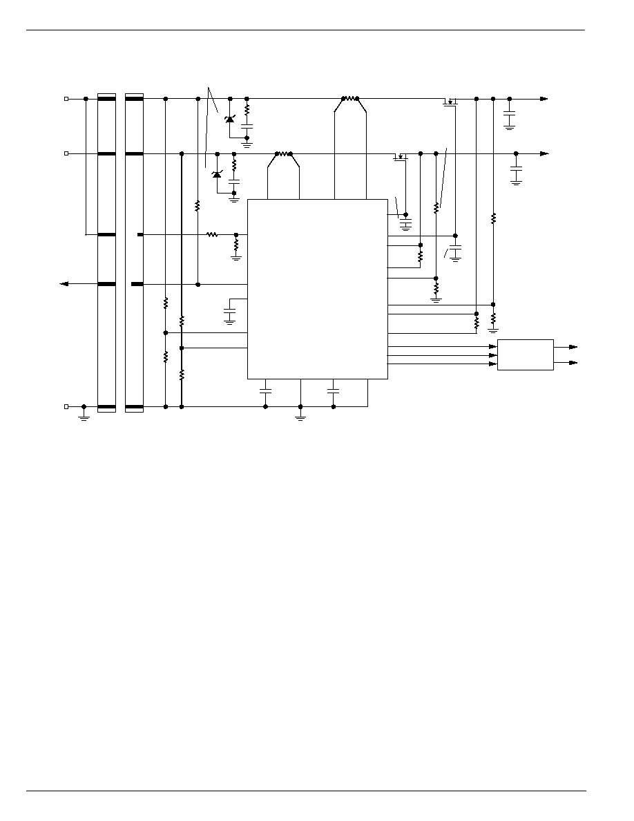
Typical Application
*C5
0.047
µ
F
D2
R6
130k
1%
R8
30.9k
1%
R9
8.06k
1%
R7
13k
1%
R3
47k
R4
22k
R2
10
R5
22k
V
CC1
12V
V
CC2
3.3V
GND
PCB EDGE
CONNECTOR
**BZX84Cxx
BACKPLANE
CONNECTOR
DOWNSTREAM
CONTROLLER(S)
Downstream Control Signals
SENSE2
VCC2
R
SENSE2
0.020
1
2
3
4
1
2
SENSE1
VCC1
R
SENSE1
0.006
1
2
3
4
24
23
C3
0.01
µ
F
Q2
Si7892DP
(PowerPAKTM SO-8)
C
LOAD1
330
µ
F
V
OUT1
12V
6A
V
OUT2
3.3V
1.5A
C
LOAD2
330
µ
F
C4
0.01
µ
F
Q1
Si7892DP
(PowerPAKTM SO-8)
C7
0.033
µ
F
C6
0.02
µ
F
CPOR
CFILTER
GND
3
22
5
6
7
20
18
19
17
16
15
11
TRK
9
13
10
GATE2
GATE1
OUT2
DIS2
DIS1
FB2
FB1
/POR
PG2
PG1
OUT1
CDLY
12
/FAULT
14
OV1
21
OV2
4
ON
8
Undervoltage (Output1) = 10.5V
Undervoltage (Output2) = 2.95V
Overvoltage (Input1) = 13.2V
Overvoltage (Input2) = 3.65V
START-UP Delay = 2.5ms
POR Delay = 10ms
Circuit Breaker Response Time = 16ms
*C5 (optional) is used to set the delay for V
OUT2
with respect to V
OUT1
V
OUT2
Delay = 9.5ms
**D1 is BZX84C18 and D2 is BZX84C8V2
Resistor tolerances are 5% unless specified otherwise.
C2
0.47
µ
F
R11
120
R15
4.42k
1%
R13
14.7k
1%
R10
560
R12
105k
1%
R14
10.7k
1%
D1
R1
10
C1
0.47
µ
F
/FAULT
Signal
MIC2585-1
Figure 1. Typical Application Circuit
March 2003
3
MIC2584/2585
MIC2584/2585
Micrel
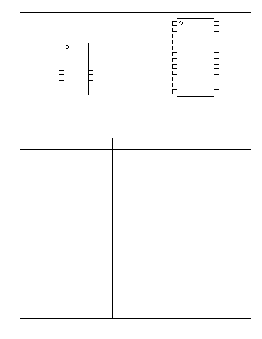
Pin Configuration
1
VCC2
SENSE2
GATE2
OUT2
FB2
ON
CPOR
CFILTER
16 VCC1
SENSE1
GATE1
OUT1
FB1
/POR
/FAULT
GND
15
14
13
12
11
10
9
2
3
4
5
6
7
8
MIC2584
16-Pin TSSOP (TS)
CDLY
GND
13
12
CFILTER
/FAULT
14
11
1
VCC2
SENSE2
GATE2
OV2
OUT2
DIS2
FB2
ON
TRK
CPOR
24 VCC1
SENSE1
GATE1
OV1
OUT1
DIS1
FB1
PG1
PG2
/POR
23
22
21
20
19
18
17
16
15
2
3
4
5
6
7
8
9
10
MIC2585
24-Pin TSSOP (TS)
Pin Description
Pin Number
Pin Number
Pin Name
Pin Function
MIC2584
MIC2585
16
24
VCC1
Positive Supply (Input), Channel 1: This input is the main supply to the
internal circuitry and must be in the range of 2.3V to 13.2V. The GATE1 pin
is held low by an internal undervoltage lockout circuit until V
CC1
and V
CC2
exceed their respective undervoltage lockout threshold of 2.165V and 0.8V.
This input is protected up to 20V.
1
1
VCC2
Positive Supply (Input), Channel 2: The GATE2 pin is held low by an
internal undervoltage lockout circuit until V
CC1
and V
CC2
exceed their
respective undervoltage lockout threshold of 2.165V and 0.8V. This input
must be in the range of 1.0V to 13.2V and less than or equal to V
CC1
. This
input is protected up to 20V.
2, 15
2, 23
SENSE2, SENSE1
Circuit Breaker Sense (Inputs): A resistor between this pin and VCC1 and
VCC2 sets the current limit threshold for each channel. Whenever the
voltage across either sense resistor exceeds the slow trip current limit
threshold (V
TRIPSLOW
), the GATE voltage is adjusted to ensure a constant
load current. If V
TRIPSLOW
(50mV) is exceeded for longer than time period
t
OCSLOW
, then the circuit breaker is tripped and both GATE outputs are
immediately pulled low. If the voltage across either sense resistor exceeds
the fast trip circuit breaker threshold, V
TRIPFAST
, at any point due to fast,
high amplitude power supply faults, then both GATE outputs are immediately
brought low without delay. To disable the circuit breaker for either channel,
the SENSE and VCC pins can be tied together.
The default V
TRIPFAST
for either device is 100mV. Other fast trip thresholds
are available: 150mV, 200mV, or OFF (V
TRIPFAST
disabled). Please contact
factory for availability of other options.
6
8
ON
Enable (Input): Active High. The ON pin, an input to a Schmitt-triggered
comparator used to enable/disable the controller, is compared to a 1.235V
reference with 25mV of hysteresis. When a logic high is applied to the ON
pin (V
ON
> 1.235V), a start-up sequence begins when the GATE1 and
GATE2 pins begin ramping up towards their final operating voltage. When
the ON pin receives a logic low signal (V
ON
< 1.21V), the GATE pins are
grounded and /FAULT remains high if both inputs are above their respective
UVLO thresholds. The ON pin must be low for at least 20
µ
s in order to
initiate a start-up sequence. Additionally, toggling the ON pin LOW to HIGH
resets the circuit breaker.

MIC2584/2585
Micrel
MIC2584/2585
4
March 2003
Pin Number
Pin Number
Pin Name
Pin Function
MIC2584
MIC2585
3, 14
3, 22
GATE2, GATE1
Gate Drive (Outputs): Connect each output to the gates of external
N-Channel MOSFETs. When ON is asserted, a 14
µ
A current source is
activated and begins to charge the gate of the N-Channel MOSFET connected
to this pin. An internal clamp ensures that no more than 10V is applied
between the GATE and Source when VCC1 or VCC2 is above 5V. When the
circuit breaker trips or when an input undervoltage lockout condition is
detected, the GATE1 and GATE2 pins are immediately brought low.
9
13
GND
Ground: Tie to analog ground.
7
10
CPOR
Power-On Reset Timer (Input): A capacitor connected between this pin and
ground sets the start-up delay (t
START
) and the power-on reset interval
(t
POR
). Once the lagging supply rises above its UVLO threshold and ON
asserts, the capacitor connected to CPOR begins to charge. When the
voltage at CPOR crosses 0.3V, the start-up threshold (V
START
), a start cycle
is initiated as the GATE outputs begin to ramp while capacitor C
POR
is
immediately discharged to ground. When the voltage at the lagging FB pin
rises above its threshold (V
FB
), capacitor CPOR begins to charge again.
When the voltage at CPOR rises above the power-on reset delay threshold
(V
POR
) of 1.235V, the timer resets by pulling CPOR to ground and /POR is
deasserted. If C
POR
= 0, then t
START
defaults to 20
µ
s.
8
11
CFILTER
Current Limit Response Timer (Input): A capacitor connected to this pin
defines the period of time, t
OCSLOW
, in which an overcurrent event must last
to signal a fault condition and trip the circuit breaker. When an overcurrent
condition occurs, a 2.5
µ
A current source begins to charge this capacitor. If
the voltage at this pin reaches 1.235V, the circuit breaker is tripped, both
GATE pins immediately shut off, and /FAULT is asserted. If C
FILTER
= 0,
then t
OCSLOW
defaults to 20
µ
s.
5, 12
7, 18
FB2, FB1
Power-Good Threshold Input (Undervoltage Detect): FB1 and FB2 are
internally compared to 1.235V and 0.80V references with 25mV of hyster-
esis, respectively. External resistive divider networks may be used to set the
voltage at these pins. If either FB input momentarily goes below its thresh-
old, then /POR is activated for one timing cycle, t
POR
, indicating an output
undervoltage condition. The /POR signal deasserts one timing cycle after the
FB pin exceeds its power-good threshold by 25mV. A 5
µ
s filter on these pins
prevents glitches from inadvertently activating the /POR signal.
10
14
/FAULT
Circuit Breaker Fault Status (Output): Active-Low, weak pull-up to VCC1 or
open-drain. Asserted when the circuit breaker is tripped due to an
overcurrent, undervoltage lockout, or overvoltage event. When deasserted,
the MIC2585 will initiate a new start cycle by toggling the ON pin.
11
15
/POR
Power-On Reset (Output): Active Low, weak pull-up to VCC1 or open drain.
This pin remains asserted during start-up until a time period (t
POR
) after the
lagging FB pin threshold (V
FB1
or V
FB2
) is exceeded. The timing capacitor
C
POR
determines t
POR
. When the output voltage monitored at either FB pin
falls below V
FB
, /POR is asserted for a minimum of one timing cycle (t
POR
).
4, 13
5, 20
OUT2, OUT1
Output Voltage Monitor (Inputs): For output tracking, connect these pins to
their respective output to sense the output voltage.
N/A
12
CDLY
Output Sequence Delay Timer (Input): This pin is internally clamped to 6V.
A capacitor connected to this pin sets a timer delay, t
DLY
, between V
OUT1
and V
OUT2
as shown in Figure 5. With this pin pulled up to VCC1 through a
resistor, and if C
GATE1
= C
GATE2
, both V
OUT1
and V
OUT2
ramp up and down
with the same dv/dt as depicted in the Tracking Mode diagram while
maintaining a maximum voltage differential between V
OUT1
and V
OUT2
.
N/A
9
TRK
Discharge Tracking Mode Pin (Input): Tie this pin to OUT1 or OUT2 to
enable tracking during turn-off cycle. Ground this pin to disable tracking
during turn-off. The TRK pin is not to be used as a digital input.

March 2003
5
MIC2584/2585
MIC2584/2585
Micrel
Pin Number
Pin Number
Pin Name
Pin Function
MIC2584
MIC2585
N/A
4, 21
OV2, OV1
Overvoltage Detect Inputs: Whenever the threshold voltage (V
OV1
, V
OV2
) on
either input is exceeded, the circuit-breaker is tripped while /FAULT is
asserted and the GATE1 and GATE2 outputs are immediately brought low.
N/A
6, 19
DIS2, DIS1
Discharge Outputs: When the ON pin receives a logic low signal
(deasserts), these pins provide a low impedance path to ground in order to
allow the discharging of any load capacitance. The DIS pins assert low if
TRK is less than 0.3V once ON has been deasserted. The typical DIS pin
resistance varies between 50
to 170
dependent upon input supply
voltage (see Electrical Table). An external resistor is required. See "
Fast
Output Discharge for Capacitive Load
" section in the Applications Informa-
tion for more detail.
N/A
16, 17
PG2, PG1
Power-Good Outputs: Active-HIGH, weak pull-up to VCC1 or open-drain.
These outputs are asserted whenever the FB1 and FB2 thresholds are
exceeded and will not be asserted when FB1 and FB2 are below their
thresholds.