August 2002
1
MIC2590B
MIC2590B
Micrel
MIC2590B
Dual-Slot PCI Hot Plug Controller
Final Information
General Description
The MIC2590B is a power controller supporting power distri-
bution requirements for Peripheral Component Interconnect
(PCI) hot plug compliant systems incorporating the Intelligent
Platform Management Interface (IPMI). The MIC2590B pro-
vides complete power control support for two PCI slots
including the 3.3V
AUX
defined by the PCI 2.2 specification.
Support for +5V, +3.3V, +12V and 12V supplies is provided
including programmable constant-current inrush limiting,
voltage supervision, programmable current limit, fault report-
ing and circuit breaker functions which provide fault isolation.
The MIC2590B also incorporates a SMBus interface in which
complete status and control of power within each slot is
provided. Data such as voltage and current from each supply
of each slot can be obtained for IPMI sensor records in
addition to power status of each slot.
Features
· Supports two independent PCI 2.2 slots
· SMBus interface for slot power control and status
· +5V, +3.3V, +12V, 12V, +3.3V
AUX
supplies supported
per PCI specification 2.2
· Programmable inrush current-limiting
· Active current regulation controls inrush current
· Electronic circuit breaker
· Dual level fault detection for quick fault response without
nuisance tripping
· Thermal isolation between circuitry for slot A
and slot B
Applications
· PCI hot-plug power distribution
Micrel, Inc. · 1849 Fortune Drive · San Jose, CA 95131 · USA · tel + 1 (408) 944-0800 · fax + 1 (408) 944-0970 · http://www.micrel.com
Ordering Information
5V & 3V Fast-trip
+12V & 12V Fast-trip
Part Number
Threshold
Threshold
Operating Temp. Range
Package
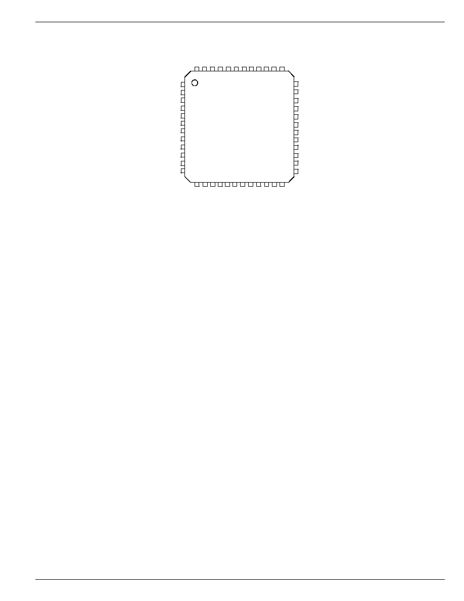
MIC2590B-2BTQ
100mV
1.5A/0.4A
0
°C to +70°C
48-Pin TQFP
MIC2590B-5BTQ
Disabled*
1.5A/0.4A
0
°C to +70°C
48-Pin TQFP
*Contact factory for availability.
MIC2590B
Micrel
MIC2590B
4
August 2002
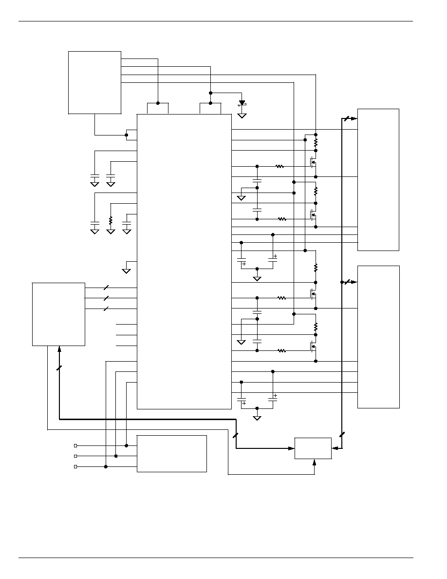
Pin Description
Pin Number
Pin Name
Pin Function
6, 31
5VINA, 5VINB
5V Supply Power and Sense Inputs [A/B]: Two pins are provided for Kelvin
connection (one for each slot). Pin 6 is the Kelvin sense connection to the
supply side of the sense resistor for 5V Slot A. Pin 31 is the Kelvin sense
connection to the supply side of the sense resistor for 5V Slot B. These two
pins must ultimately connect to each other within 10cm. An undervoltage
lockout circuit (UVLO) prevents the switches from turning on while this input is
less than its lockout threshold.
12, 25
3VINA, 3VINB
3.3V Supply Power and Sense Inputs [A/B]: Two pins are provided for
Kelvin connection (one for each slot). Pin 12 is the Kelvin sense connection to
the supply side of the sense resistor for 3V Slot A. Pin 25 is the Kelvin sense
connection to the supply side of the sense resistor for 3V Slot B. These two
pins must ultimately connect to each other within 10cm. An undervoltage
lockout circuit (UVLO) prevents the switches from turning on while this input is
less than its lockout threshold.
5, 32
12VIN 2 pins
+12V Supply Input: An undervoltage lockout circuit prevents the switches from
turning on while this input is less than its lockout threshold. Both pins must be
tied together at the chip.
17,18
12VMIN 2 pins
12V Supply Input: An undervoltage lockout circuit prevents the switches from
turning on while this input is less than its lockout threshold. Both pins must be
tied together at the chip.
10, 27
12VOUTA, 12VOUTB
12V output [A/B]
19, 20
12MVOUTA, 12MVOUTB
12V output [A/B]
3, 34
12VSLEWA, 12VSLEWB
12V Slew Rate Control [A/B]: Connect capacitors between these pins and
ground to set output slew rates of the +12V and -12V supplies.
45, 42
AUXENA, AUXENB
AUX Enable Inputs [A/B]: Rising-edge sensitive enable inputs for VAUXA
and VAUXB outputs. Taking AUXENA/AUXENB low after a fault resets the
respective slot's Aux Output Fault Latch. Tie these pins to ground if using
SMBus-mode power control.
16, 21
3VOUTA, 3VOUTB
3.3V Power-Good Sense Inputs: Connect to 3.3V[A/B] outputs. Used to
monitor the 3.3V output voltages for Power-Good status.
9, 28
5VOUTA, 5VOUTB
5V Power-Good Sense Inputs: Connect to 5V[A/B] outputs. Used to monitor
the 5V output voltages for Power-Good status.
33
IREF
A resistor connected between this pin and ground sets the ADC current
measurement gain. This resistor must be 20k
±1%.
7, 30
5VSENSEA, 5VSENSEB
5V Circuit Breaker Sense Input [A/B]: The current-limit thresholds are set by
connecting sense resistors between these pins and 5VIN[A/B]. When the
current-limit threshold of IR = 50mV is reached, the 5VGATE[A/B] pin is
modulated to maintain a constant voltage across the sense resistor and
therefore a constant current into the load. If the 50mV threshold is exceeded
for t
FLT
, the circuit breaker is tripped and the GATE pin for the affected slot is
immediately pulled low.
13, 24
3VSENSEA, 3VSENSEB
3V Circuit Breaker Sense Input [A/B]: The current limit thresholds are set by
connecting sense resistors between these pins and 3VIN[A/B]. When the
current limit threshold of IR = 50mV is reached, the 3VGATE[A/B] pin is
modulated to maintain a constant voltage across the sense resistor and
therefore a constant current into the load. If the 50mV threshold is exceeded
for t
FLT
, the circuit breaker is tripped and the GATE pin for the affected slot is
immediately pulled low.
August 2002
5
MIC2590B
MIC2590B
Micrel
Pin Description
Pin Number
Pin Name
Pin Function
8, 29
5VGATEA, 5VGATEB
5V Gate Drive Outputs [A/B]: Each connects to the gate of an external N-
Channel MOSFET. During power-up the C
GATE
and the gate of the
MOSFETs are charged by a 20
µA current source. This controls the value of
dv/dt seen at the source of the MOSFETs, and hence the current flowing into
the load capacitance.
During current limit events, the voltage at this pin is adjusted to maintain
constant current through the switch for a period of t
FLT
. Whenever an
overcurrent, thermal shutdown or input undervoltage fault condition occurs
the GATE pin for the affected slot is immediately brought low.
During power-down these pins are discharged by an internal current source.
14, 23
3VGATEA, 3VGATEB
3V Gate Drive Outputs [A/B]: Each connects to the gate of an external N-
Channel MOSFET. During power-up the C
GATE
and the gate of the
MOSFETs are charged by a 20
µA current source. This controls the value of
dv/dt seen at the source of the MOSFETs, and hence the current flowing into
the load capacitance.
During current limit events, the voltage at this pin is adjusted to maintain
constant current through the switch for a period of t
FLT
. Whenever an
overcurrent, thermal shutdown or input undervoltage fault condition occurs
the GATE pin for the affected slot is immediately brought low.
During power-down these pins are discharged by an internal current source.
11, 26
VSTBY 2 pins
3.3V Standby input voltage required to support PCI 2.2 VAUX input: SMBus,
internal registers and A/D converter run off of VSTBY to ensure chip access
during standby modes. A UVLO circuit prevents turn-on of this supply until
VSTBY rises above its UVLO threshold. Both pins must be tied together at
the chip.
15, 22
VAUXA, VAUXB
V
AUX
[A/B] output voltages to PCI card slots: These outputs connect the
VAUX pin of the PCI 2.2 Connectors VSTBY via internal 400m
MOSFETs
which are current-limited and protected against short circuit faults.
44, 43
ONA, ONB
Enable input for MAIN outputs: Rising-edge sensitive. Used to enable or
disable MAIN (5V, 3.3V, +12V, 12V) outputs. Taking ONA/ONB low after a
fault resets the respective slot's Main Output Fault Latch. Tie these pins to
ground if using SMBus-mode power control.
1, 36
/FAULTA, /FAULTB
Open Drain, Active-Low: Asserted whenever the circuit breaker trips due to
a fault condition.
/FAULT[A/B] is reset by bringing the faulted slot's ON pin low if /FAULT was
asserted in response to a fault condition on one of the slot's MAIN outputs
(+12V, +5V, +3.3V, or 12V).
/FAULT[A/B] is reset by bringing the faulted slot's AUXEN pin low if /FAULT
was asserted in response to a fault condition on the slot's VAUX output.
If a fault condition occurred on both the MAIN and AUX outputs of the same
slot, then both ON and AUXEN must be brought low to de-assert the /FAULT
output.
2, 35
CFILTERA, CFILTERB
Filter Capacitor [A/B]: Capacitors connected between these pins and ground
set the duration of t
FLT
. t
FLT
is the amount of time for which a slot remains in
current-limit before its circuit breaker is tripped.
37
/INT
Interrupt Output: Open Drain, Active-low. Asserted whenever a power fault
is detected. Cleared by writing a logic 1 to the respective active bit into the
Status Register.