November 2004
1
MIC280
MIC280
Micrel
MIC280
Precision IttyBittyTM Thermal Supervisor
REV. 11/04
General Description
The MIC280 is a digital thermal supervisor capable of measur-
ing its own internal temperature and that of a remote PN junc-
tion. The remote junction may be an inexpensive commodity
transistor, e.g., 2N3906, or an embedded thermal diode such
as found in Intel Pentium* II/III/IV CPUs, AMD Athlon* CPUs,
and Xilinx Virtex* FPGA's. A 2-wire SMBus* 2.0 compatible
serial interface is provided for host communication. Remote
temperature is measured with ±1∞C accuracy and 9-bit to
12-bit resolution (programmable). Independent high, low, and
over-temperature thresholds are provided for each zone.
The advanced integrating A/D converter and analog front-end
reduce errors due to noise for maximum accuracy and mini-
mum guardbanding. The interrupt output signals temperature
events to the host, including data-ready and diode faults.
Critical device settings can be locked to prevent changes and
insure failsafe operation. The clock, data, and interrupt pins
are 5V-tolerant regardless of the value of V
DD
. They will not
clamp the bus lines low even if the device is powered down.
Superior accuracy, failsafe operation, and small size make
the MIC280 an excellent choice for the most demanding
thermal management applications.
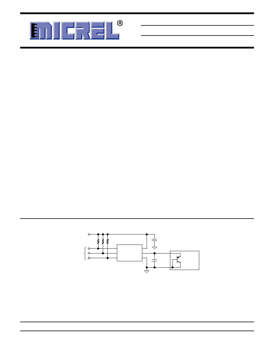
Typical Application
DATA
5
4
6
2
3
1
TO
SERIAL BUS
HOST
2N3906/
CPU DIODE
1800pF
MIC280
CLK
/INT
3V to 3.6V
3 ◊
10k
VDD
T1
GND
0.1µF
ceramic
MIC280 Typical Application
Features
∑ Measures local and remote temperature
∑ Highly accurate remote sensing
±1∞C max., 60∞C to 100∞C
∑ Superior noise immunity for reduced temperature guard-
bands
∑ 9-bit to 12-bit temperature resolution for remote zone
∑ Fault queues to further reduce nuisance tripping
∑ Programmable high, low, and over-temperature thresh-
olds for each zone
∑ SMBus 2 compatible serial interface including device
timeout to prevent bus lockup
∑ Voltage tolerant I/O's
∑ Open-drain interrupt output pin - supports SMBus Alert
Response Address protocol
∑ Low power shutdown mode
∑ Locking of critical functions to insure failsafe operation
∑ Failsafe response to diode faults
∑ Enables ACPI compliant thermal management
∑ 3.0V to 3.6V power supply range
∑ IttyBittyTM SOT23-6 package
Applications
∑ Desktop, server and notebook computers
∑ Printers and copiers
∑ Test and measurement equipment
∑ Thermal supervision of Xilinx Virtex FPGA's
∑ Wireless/RF systems
∑ Intelligent power supplies
∑ Datacom/telecom cards
Micrel, Inc. ∑ 2180 Fortune Drive ∑ San Jose, CA 95131 ∑ USA ∑ tel + 1 (408) 944-0800 ∑ fax + 1 (408) 474-1000 ∑ http://www.micrel.com
IttyBiity is a trademark of Micrel, Inc.
*All trademarks are the property of their respective owners.
MIC280
Micrel
MIC280
2
November 2004
Pin Configuration
1
VDD
GND
T1
6
5
/INT
DATA
CLK
4
2
3
SOT23-6
Pin Description
Pin Number
Pin Name
Pin Function
1
VDD
Power Supply Input.
2
GND
Ground.
3
T1
Analog Input. Connection to remote diode junction.
4
CLK
Digital Input. Serial bit clock input.
5
DATA
Digital Input/Output. Open-drain. Serial data input/output.
6
/INT
Digital Output. Open-drain. Interrupt output.
Ordering Information
Part Number
Slave Address Ambient Temp. Range
Package
Standard
Marking Pb-FREE
Marking
MIC280-0BM6
TA00
MIC280-0YM6
TA00
100 1000
b
-55∞C to +125∞C
SOT23-6
MIC280-1BM6
TA01
MIC280-1YM6
TA01
100 1001
b
-55∞C to +125∞C
SOT23-6
MIC280-2BM6
TA02
MIC280-2YM6
TA02
100 1010
b
-55∞C to +125∞C
SOT23-6
MIC280-3BM6
TA03
MIC280-3YM6
TA03
100 1011
b
-55∞C to +125∞C
SOT23-6
MIC280-4BM6 TA04
MIC280-4YM6
TA05
100 1100
b
-55∞C to +125∞C
SOT23-6
MIC280-5BM6 TA05
MIC280-5YM6
TA05
100 1101
b
-55∞C to +125∞C
SOT23-6
MIC280-6BM6 TA06
MIC280-6YM6
TA06
100 1110
b
-55∞C to +125∞C
SOT23-6
MIC280-7BM6 TA07
MIC280-7YM6
TA07
100 1111
b
-55∞C to +125∞C
SOT23-6

November 2004
3
MIC280
MIC280
Micrel
Absolute Maximum Ratings
(Note 1)
Power Supply Voltage, V
DD .....................................................
3.8V
Voltage on T1 ........................................≠0.3V to V
DD
+0.3V
Voltage on CLK, DATA, /INT ..............................≠0.3V to 6V
Current Into Any Pin ................................................. ±10mA
Power Dissipation, T
A
= 125∞C ................................ 109mW
Storage Temperature ................................ ≠65∞C to +150∞C
ESD Ratings,
Note 3
Human Body Model ................................................ 1.5kV
Machine Model ........................................................ 200V
Soldering (SOT23-6 Package)
Vapor Phase (60s) .....................................220∞C
+5
/
-0
∞C
Infrared (15s) .............................................235∞C
+5
/
-0
∞C
Operating Ratings
(Note 2)
Power Supply Voltage, V
DD
............................ +3V to +3.6V
Ambient Temperature Range (T
A
) .......... ≠55∞C to +125∞C
Junction Temperature ................................................ 150∞C
Package Thermal Resistance (
JA
)
SOT23-6 ............................................................230∞C/W
Electrical Characteristics
For typical values T
A
= 25∞C, V
DD
= 3.3V, unless otherwise noted.
Bold values indicate ≠55∞C T
A
125∞C, 3.0V V
DD
3.6V,
unless otherwise noted. Note 2
Symbol
Parameter
Conditions
Min.
Typ
Max
Units
Power Supply
I
DD
Supply Current
/INT, T1 open; CLK = DATA = High;
0.23
0.4
mA
Normal Mode
Shutdown Mode; /INT, T1 open;
Note 5
9
µ
A
CLK = 100kHz, DATA = High
Shutdown Mode; /INT, T1 open;
6
[TBD]
µ
A
CLK = DATA = High
t
POR
Power-on Reset Time,
Note 5
V
DD
> V
POR
200
µ
s
V
POR
Power-on Reset Voltage
All registers reset to default values;
2.65
2.95
V
A/D conversions initiated
V
HYST
Power-on Reset Hysteresis Voltage
300
mV
Note 5
Temperature-to-Digital Converter Characteristics
Accuracy, Remote Temperature
60∞C T
D
100∞C,
±0.25
±1
∞C
Notes 2, 7, 10, 11
3.15V < V
DD
< 3.45V, 25∞C < T
A
< 85∞C
0∞C T
D
100∞C,
±1
±2
∞C
3.15V < V
DD
< 3.45V, 25∞C < T
A
< 85∞C
≠55∞C T
D
125∞C,
±2
±4
∞C
3.15V < V
DD
< 3.45V, 25∞C < T
A
< 85∞C
Accuracy, Local Temperature
0∞C T
A
100∞C, 3.15V < V
DD
< 3.45V
±1
±2
∞C
Note 2, 10
≠55∞C T
A
125∞C, 3.15V < V
DD
< 3.45V
±1.5
±2.5
∞C
t
CONV
Conversion Time, Notes 2, 8
RES[1:0]=00 (9 bits)
200
240
ms
RES[1:0]=01 (10 bits)
330
390
ms
RES[1:0]=10 (11 bits)
570
670
ms
RES[1:0]=11 (12 bits)
1000
1250
ms
Remote Temperature Input, T1
I
F
Current into External Diode
T1 forced to 1.0V, High level
192
400
µ
A
Note 5
Low level
7
12
µ
A

MIC280
Micrel
MIC280
4
November 2004
Symbol
Parameter
Condition
Min
Typ
Max
Units
Serial Data I/O Pin, DATA
V
OL
Low Output Voltage, Note 4
I
OL
= 3mA
0.3
V
I
OL
= 6mA
0.5
V
V
IL
Low Input Voltage
3V V
DD
3.6V
0.8
V
V
IH
High Input Voltage
3V V
DD
3.6V
2.1
5.5
V
C
IN
Input Capacitance
Note 5
10
pF
I
LEAK
Input Current
±1
µ
A
Serial Clock Input, CLK
V
IL
Low Input Voltage
3V V
DD
3.6V
0.8
V
V
IH
High Input Voltage
3V V
DD
3.6V
2.1
5.5
V
C
IN
Input Capacitance
Note 5
10
pF
I
LEAK
Input Current
±1
µ
A
Interrupt Output, /INT
V
OL
Low Output Voltage, Note 4
I
OL
= 3mA
0.3
V
I
OL
= 6mA
0.5
V
t
INT
Interrupt Propagation Delay
from TEMPx < TLOWx or
[t
CONV
]
ms
Notes 5, 6
TEMPx > THIGHx or TEMPx >
CRITx to /INT < V
OL
; R
PULLUP
= 10k
t
nINT
Interrupt Reset Propagation Delay
from read of STATUS or A.R.A. to
1
µ
s
Note 5, 9
/INT > V
OH
; R
PULLUP
= 10k
I
LEAK
±1
µ
A
Serial Interface Timing
t
1
CLK (Clock) Period
2.5
µs
t
2
Data In Setup Time to CLK High
100
ns
t
3
Data Out Stable after CLK Low
300
ns
t
4
Data Low Setup Time to CLK Low
Start Condition
100
ns
t
5
Data High Hold Time after CLK
Stop Condition
100
ns
High
t
TO
Bus Timeout
25
30
35
ms
Note 1. Exceeding the absolute maximum rating may damage the device.
Note 2. The device is not guaranteed to function outside its operating range. Final test on outgoing product is performed at T
A
= 25∞C.
Note 3. Devices are ESD sensitive. Handling precautions recommended.
Note 4. Current into the /INT or DATA pins will result in self heating of the device. Sink current should be minimized for best accuracy.
Note 5. Guaranteed by design over the operating temperature range. Not 100% production tested.
Note 6. t
INT
and t
CRIT
are equal to t
CONV
.
Note 7. T
D
is the temperature of the remote diode junction. Testing is performed using a single unit of one of the transistors listed in Table 8.
Note 8. t
CONV
= t
CONV
(local) + t
CONV
(remote). Following the acquisition of either remote or local temperature data, the limit comparisons for that zone
are performed and the device status updated; Status bits will be set and /INT driven active, if applicable.
Note 9. The interrupt reset propogation delay is dominated by the capacitance on the bus.
Note 10. Accuracy specification does not include quantization noise, which may be up to ±
1
/
2
LSB.
Note 11. Tested at 10-bit resolution.

November 2004
5
MIC280
MIC280
Micrel
Timing Diagrams
t
1
t
2
t
5
t
4
t
3
CLK
DATA INPUT
DATA OUTPUT
Serial Interface Timing
MIC280
Micrel
MIC280
6
November 2004
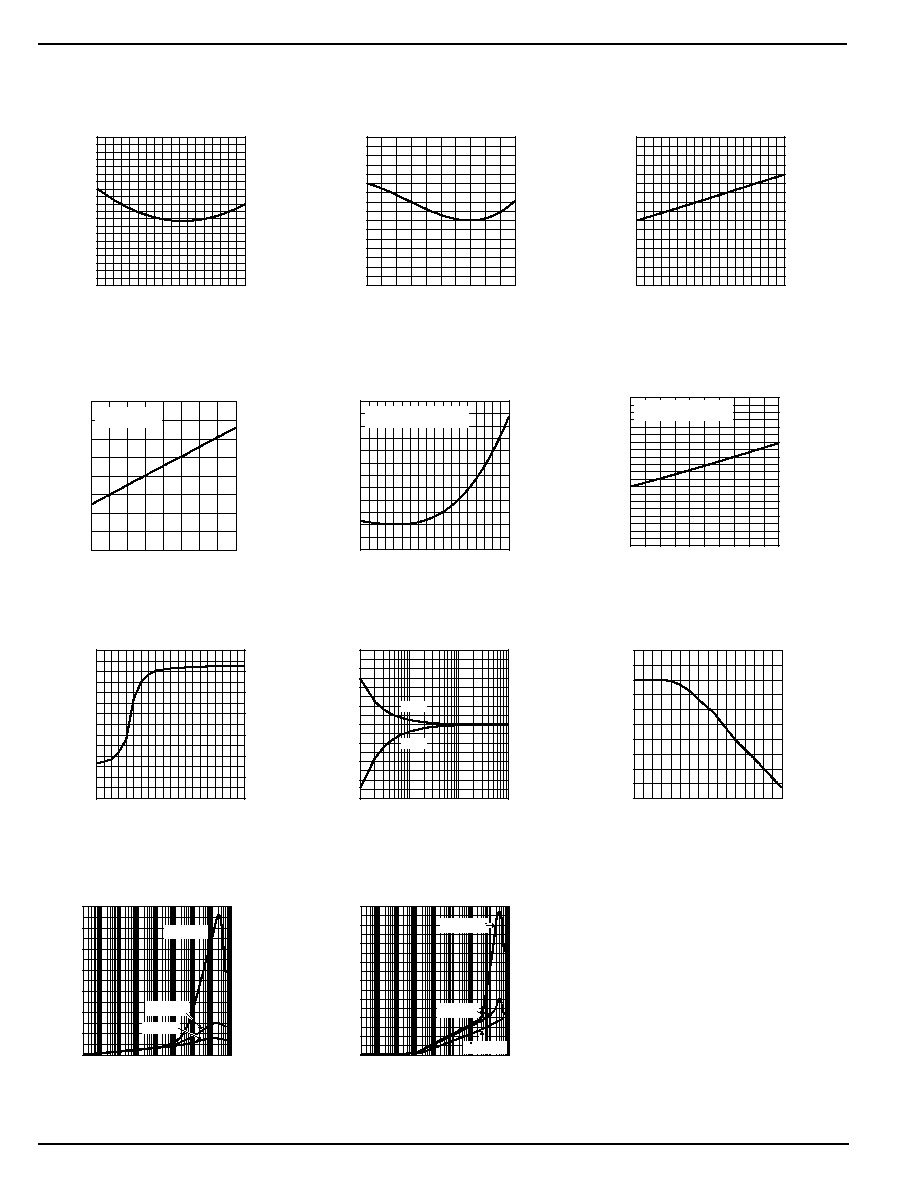
Typical Characteristics
V
DD
= 3.3V; T
A
= 25∞C, unless otherwise noted.
-2.5
-2
-1.5
-1
-0.5
0
0.5
1
1.5
2
2.5
-55 -35 -15 5 25 45 65 85 105 125
MEASURMENT ERROR
(
∞
C)
JUNCTION TEMPERATURE (∞C)
A ccuracy vs .
T emperature, Internal S ens or
0
20
40
60
80
100
120
140
0 1 2 3 4 5 6 7 8 9 10
MEASURED LOCAL TEMPERATURE
(
∞
C)
TIME (sec)
R es pons e to Immers ion
in 125∞C F luid B ath
-20
-15
-10
-5
0
5
0
1000
2000
3000
4000
5000
6000
7000
8000
TEMPERATURE ERROR
(
∞
C)
CAPACITANCE (pF)
R emote T emperature E rror vs .
C apacitanc e on T 1
-2
-1.5
-1
-0.5
0
0.5
1
1.5
2
0
20
40
60
80
100
MEASUREMENT ERROR
(
∞
C)
REMOTE DIODE TEMPERATURE (∞C)
R emote T emperature
Meas urement E rror
0
50
100
150
200
250
300
350
400
-55 -35 -15 5 25 45 65 85 105 125
SUPPLY CURRENT
(
µ
A)
TEMPERATURE (∞C)
S upply C urrent vs .
T emperature for V
DD
= 3.3V
0
5
10
15
20
25
30
-55 -35 -15 5 25 45 65 85 105 125
QUIESCENT CURRENT
(
µ
A)
TEMPERATURE (∞C)
Quies c ent C urrent vs .
T emperature in S hutdown Mode
/INT , T 1 open
C LK = DAT A = HIG H
0
1
2
3
4
5
6
7
8
9
10
2.6
2.8
3.0
3.2
3.4
3.6
QUIESCENT CURRENT
(
µ
A)
SUPPLY VOLTAGE (V)
Quies c ent C urrent vs .
S upply V oltage in S hutdown Mode
/INT , T 1 open
C LK = DAT A = HIG H
0
5
10
15
20
0
100
200
300
400
QUIESCENT CURRENT
(
µ
A)
FREQUENCY (kHz)
Quies cent C urrent vs .
C loc k F requency in
S hutdown Mode
/INT , T 1 open
DAT A = HIG H
-8
-6
-4
-2
0
2
4
6
8
1x10
6
1x10
7
1x10
8
1x10
9
MEASUREMENT ERROR
(
∞
C)
RESISTANCE FROM T1 ()
Meas urement E rror vs .
P C B L eakage to +3.3V /G ND
G ND
3.3V
0
1
2
3
4
5
6
7
REMOTE TEMP. ERROR
(
∞
C)
Nois e Injected into the B as e of
R emote T rans is tor
FREQUENCY (Hz)
1 10 100 1k 10k 100k 1M 10M100M
3mV
P -P
25mV
P -P
10mV
P -P
0
0.2
0.4
0.6
0.8
1.0
1.2
1.4
1.6
TEMPERTURE ERROR
(
∞
C)
Nois e Injected into the
C ollec tor of R emote T rans is tor
FREQUENCY (Hz)
1 10 100 1k 10k 100k 1M 10M100M
50mV
P -P
25mV
P -P
100mV
P -P
November 2004
7
MIC280
MIC280
Micrel
Functional Description
Serial Port Operation
The MIC280 uses standard SMBus Write_Byte, Read_Byte,
and Read_Word operations for communication with its host.
The SMBus Write_Byte operation involves sending the
device's slave address (with the R/W bit low to signal a write
operation), followed by a command byte and the data byte.
The SMBus Read_Byte operation is a composite write and
read operation: the host first sends the device's slave address
followed by the command byte, as in a write operation. A
new start bit must then be sent to the MIC280, followed by a
repeat of the slave address with the R/W bit (LSB) set to the
high (read) state. The data to be read from the part may then
be clocked out. A Read_Word is similar, but two successive
data bytes are clocked out rather than one. These protocols
are shown in Figure 1, Figure 2, and Figure 3.
The Command byte is eight bits (one byte) wide. This byte
carries the address of the MIC280 register to be operated
upon. The command byte values corresponding to the vari-
ous MIC280 registers are shown in Table 1. Other command
byte values are reserved, and should not be used.
Slave Address
The MIC280 will only respond to its own unique slave ad-
dress. A match between the MIC280's address and the
address specified in the serial bit stream must be made to
initiate communication. The MIC280's slave address is fixed
at the time of manufacture. Eight different slave addresses
are available as determined by the part number. See Table
2 below and the Ordering Information table above.
Part Number
Slave Address
MIC280-0BM6
100 1000
b
= 48
h
MIC280-1BM6
100 1001
b
= 49
h
MIC280-2BM6
100 1010
b
= 4A
h
MIC280-3BM6
100 1011
b
= 4B
h
MIC280-4BM6
100 1100
b
= 4C
h
MIC280-5BM6
100 1101
b
= 4D
h
MIC280-6BM6
100 1110
b
= 4E
h
MIC280-7BM6
100 1111
b
= 4F
h
Table 2: MIC280 Slave Addresses
Alert Response Address
In addition to the Read_Byte, Write_Byte, and Read_Word
protocols, the MIC280 adheres to the SMBus protocol for
response to the Alert Response Address (ARA). The MIC280
expects to be interrogated using the ARA when it has as-
serted its /INT output.
Temperature Data Format
The least-significant bit of each temperature register (high
bytes) represents one degree Centigrade. The values are in
a two's complement format, wherein the most significant bit
Command Byte
Power-on
Target Register
Value
Default
Label
Description
Read
Write
TEMP0
Local temperature result
00
h
n/a
00
h
(0∞C)
TEMP1h
Remote temperature result, high byte
01
h
n/a
00
h
(0∞C)
STATUS
Status
02
h
n/a
00
h
CONFIG
Configuration
03
h
03
h
80
h
IMASK
Interrupt mask register
04
h
04
h
07
h
THIGH0
Local temperature high limit
05
h
05
h
3C
h
(60∞C)
TLOW0
Local temperature low limit
06
h
06
h
00
h
(0∞C)
THIGH1h
Remote temperature high limit, high byte
07
h
07
h
50
h
(80∞C)
TLOW1h
Remote temperature low limit, high byte
08
h
08
h
00
h
(0∞C)
LOCK
Security register
09
h
09
h
00
h
TEMP1l
Remote temperature result, low byte
10
h
n/a
00
h
THIGH1l
Remote temperature high limit, low byte
13
h
13
h
00
h
TLOW1l
Remote temperature low limit, low byte
14
h
14
h
00
h
CRIT1
Remote over-temperature limit
19
h
19
h
64
h
(100∞C)
CRIT0
Local over-temperature limit
20
h
20
h
46
h
(70∞C)
MFG_ID
Manufacturer Identification
FE
h
n/a
2A
h
DEV_ID
Device and revision identification
FF
h
n/a
0x
h
*
* The lower nibble contains the die revision level, e.g., Rev 0 = 00h.
Table 1: MIC280 Register Addresses

MIC280
Micrel
MIC280
8
November 2004
(D7) represents the sign: zero for positive temperatures and
one for negative temperatures. Table 3 shows examples of
the data format used by the MIC280 for temperatures:
Temperature
Binary
Hex
+127∞C
0111 1111
7F
+125∞C
0111 1101
7D
+25∞C
0001 1001
19
+1∞C
0000 0001
01
0∞C
0000 0000
00
≠1∞C
1111 1111
FF
≠25∞C
1110 0111
E7
≠125∞C
1000 0011
83
≠128∞C
1000 0000
80
Table 3: Digital Temperature Format, High Bytes
Extended temperature resolution is provided for the external
zone. The high and low temperature limits and the measured
temperature for zone one are reported as 12-bit values stored
in a pair of 8-bit registers. The measured temperature, for
example, is reported in registers TEMP1h, the high-order byte,
and TEMP1l, the low-order byte. The values in the low-order
bytes are left-justified four-bit binary values representing
one-sixteenth degree increments. The A-D converter resolu-
tion for zone 1 is selectable from nine to twelve bits via the
configuration register. Low-order bits beyond the resolution
selected will be reported as zeroes. Examples of this format
are shown below in Table 4.
FAULT QUEUE
A set of fault queues (programmable digital filters) are pro-
vided in the MIC280 to prevent false tripping due to thermal
or electrical noise. Two bits, CONFIG[5:4], set the depth of
the fault queues. The fault queue setting then determines
the number of consecutive temperature events (TEMPx >
THIGHx or TEMPx < TLOWx) which must occur in order for
the condition to be considered valid. As an example, as-
sume CONFIG[5:4] is programmed with 10b. The measured
temperature for a given zone would have to exceed THIGHx
for four consecutive A/D conversions before /INT would be
asserted or the status bit set.
Like any filter, the fault queue function also has the effect
of delaying the detection of temperature events. In this ex-
ample, it would take 4 x t
CONV
to detect a temperature event.
The fault queue depth vs. CONFIG[5:4] of the configuration
register is shown in Table 5. Note: there is no fault queue
for over-temperature events (CRIT0 and CRIT1) or diode
faults. The fault queue applies only to high-temperature and
low-temperature events as determined by the THIGHx and
TLOWx registers. Any write to CONFIG will result in the fault
queues being purged and reset. Writes to any of the limit
registers, TLOWx or THIGHx, will result in the fault queue for
the corresponding zone being purged and reset.
CONFIG[5:4]
FAULT QUEUE
DEPTH
00
1 (Default)
01
2
10
4
11
6
Table 5: Fault Queue Depth Settings
Interrupt Generation
There are eight different conditions that will cause the MIC280
to set one of the bits in STATUS and assert its /INT output,
if so enabled. These conditions are listed in Table 6. Unlike
previous generations of thermal supervisor IC's, there are no
interdependencies between any of these conditions. That is,
if CONDITION is true, the MIC280 will respond accordingly,
regardless of any previous or currently pending events.
Normally when a temperature event occurs, the corresponding
status bit will be set in STATUS, the corresponding interrupt
mask bit will be cleared, and /INT will be asserted. Clearing
the interrupt mask bit(s) prohibits continuous interrupt gen-
eration while the device is being serviced. (It is possible to
prevent events from clearing interrupt mask bits by setting
bits in the lock register. See Table 7 for Lockbit function-
ality.) A temperature event will only set bits in the status
register if it is specifically enabled by the corresponding bit
in the interrupt mask register. An interrupt signal will only
be generated on /INT if interrupts are also globally enabled
(IE =1 in CONFIG).
The MIC280 expects to be interrogated using the Alert Re-
sponse Address once it has asserted its interrupt output. Fol-
lowing an interrupt, a successful response to the A.R.A. or a
read operation on STATUS will cause /INT to be de-asserted.
STATUS will also be cleared by the read operation. Reading
STATUS following an interrupt is an acceptable substitute for
Extended Temperature,
Resolution
Low Byte
9 BITS
10 BITS
11 BITS
12 BITS
Binary
Hex
Binary
Hex
Binary
Hex
Binary
Hex
0.0000
0000 0000
00
0000 0000
00
0000 0000
00
0000 0000
00
0.0625
0000 0000
00
0000 0000
00
0000 0000
00
0001 0000
10
0.1250
0000 0000
00
0000 0000
00
0010 0000
20
0010 0000
20
0.2500
0000 0000
00
0100 0000
40
0100 0000
40
0100 0000
40
0.5625
1000 0000
80
1000 0000
80
1000 0000
80
1001 0000
90
0.9375
1000 0000
80
1100 0000
C0
1110 0000
E0
1111 0000
F0
Table 4: Digital Temperature Format, Low Bytes

November 2004
9
MIC280
MIC280
Micrel
S
1
0
0
1
A2
A1
A0
0
A
X
X
X
X
X
X
X
X
A
D4
D5
D6
D3
D2
D1
D0
D7
A
P
MIC280
S
l
a
v
e
A
dd
r
es
s
D
A
T
A
CLK
C
ommand
B
y
t
e
D
a
ta
B
y
t
e
t
o MIC28
0
S
T
A
R
T
S
T
O
P
R/W = WRITE
A
CKN
O
WLEDG
E
A
CKN
O
WLEDG
E
A
CKN
O
WLEDG
E
M
as
t
er-
t
o-sl
a
v
e t
r
ansmissio
n
S
l
a
v
e-
t
o-mas
t
er
r
es
p
ons
e
Figure 1.
WRITE_BYTE Protocol
S
1
0
0
1
A2
A1
A0
A2
A1
A0
0
A
X
X
X
X
X
X
X
X
A
S
1
1
1
0
0
X
X
X
X
X
X
X
A
X
/A
P
MIC280
S
l
a
v
e
A
dd
r
es
s
D
A
T
A
CLK
C
ommand
B
y
t
e
MIC280
S
l
a
v
e
A
dd
r
es
s
D
a
ta
R
ead
F
r
om MIC28
0
S
T
A
R
T
S
T
A
R
T
S
T
O
P
R/W = WRITE
R/W = READ
A
CKN
O
WLEDG
E
A
CKN
O
WLEDG
E
A
CKN
O
WLEDG
E
N
O
T
A
CKN
O
WLEDG
E
M
as
t
er-
t
o-sl
a
v
e t
r
ansmissio
n
S
l
a
v
e-
t
o-mas
t
er
r
es
p
ons
e
Figure 2.
READ_BYTE Protocol
S
1
0
0
1
A2
A1
A0
0
A
0
0
0
0
0
0
0
1
A
MIC280
S
l
a
v
e
A
dd
r
es
s
D
A
T
A
CLK
C
ommand
B
y
t
e
S
T
A
R
T
R/W = WRITE
A
CKN
O
WLEDG
E
A
CKN
O
WLEDG
E
S
1
0
0
1
A2
A1
A0
1
A
A
D7
D8
D9
D6
D5
D4
D3
D10
D11
/A
P
D2
D1
D0
0
0
0
0
MIC280
S
l
a
v
e
A
dd
r
es
s
High-O
r
der
B
y
t
e
(
TEMP1h)
f
r
om MIC28
0
L
o
w-O
r
der
B
y
t
e
(
TEMP1L
)
f
r
om MIC28
0
S
T
A
R
T
S
T
O
P
R/W = READ
A
CKN
O
WLEDG
E
A
CKN
O
WLEDG
E
N
O
T
A
CKN
O
WLEDG
E
M
as
t
er-
t
o-sl
a
v
e t
r
ansmissio
n
S
l
a
v
e-
t
o-mas
t
er
r
es
p
ons
e
Figure 3.
READ_WORD Protocol for
Accessing TEMP1h : TEMP1l
MIC280
Micrel
MIC280
10
November 2004
S
0
0
0
1
1
0
0
1
A
/A
A2
1
0
A1
A0
0
P
0
1
A
le
r
t
R
es
p
onse
A
dd
r
es
s
D
A
T
A
/INT
MIC280
r
es
p
ond wit
h
its sl
a
v
e add
r
es
s
S
T
A
R
T
t
INT
E
v
e
n
t
O
ccur
s
S
T
O
P
R/W = READ
A
CKN
O
WLEDG
E
N
O
T
A
CKN
O
WLEDG
E
t
INT
M
as
t
er-
t
o-sl
a
v
e t
r
ansmissio
n
S
l
a
v
e-
t
o-mas
t
er
r
es
p
ons
e
Figure 4.
MIC280
Alert Response
Address Protocol
S
1
0
0
1
A2
A1
A0
0
A
A
0
0
0
0
1
1
1
0
0
X
X
X
X
X
X
X
X
/A
P
0
0
1
A2
A1
A0
1
MIC280
S
l
a
v
e
A
dd
r
es
s
D
A
T
A
/INT
C
ommand
B
y
t
e = 03
h
=
C
ONFI
G
MIC280
S
l
a
v
e
A
dd
r
es
s
V
alue in S
T
A
TUS*
*
S
T
A
R
T
t
INT
E
v
e
n
t
O
ccur
s
**
A
ll st
a
tus bits a
r
e clea
r
ed
t
o
z
e
r
o
f
oll
o
wing this o
p
e
r
a
tio
n
S
T
O
P
R/W = READ
A
CKN
O
WLEDG
E
A
CKN
O
WLEDG
E
N
O
T
A
CKN
O
WLEDG
E
M
as
t
er-
t
o-sl
a
v
e t
r
ansmissio
n
S
l
a
v
e-
t
o-mas
t
er
r
es
p
ons
e
t
INT
Figure 5.
Reading Status in response to an interrupt

November 2004
11
MIC280
MIC280
Micrel
using the A.R.A. if the host system does not implement the
A.R.A protocol. Figure 4 and Figure 5 illustrate these two
methods of responding to MIC280 interrupts.
Since temperature-to-digital conversions continue while /INT
is asserted, the measured temperature could change between
the MIC280's assertion of /INT and the host's response. It
is good practice for the interrupt service routine to read the
value in TEMPx, to verify that the over-temperature or under-
temperature condition still exists. In addition, more than one
temperature event may have occurred simultaneously or in
rapid succession between the assertion of /INT and servic-
ing of the MIC280 by the host. The interrupt service routine
should allow for this eventuality. At the end of the interrupt
service routine, the interrupt enable bits should be reset to
permit future interrupts.
Reading the Result Registers
All MIC280 registers are eight bits wide and may be accessed
using the standard Read_Byte protocol. The temperature
result for the local zone, zone 0, is a single 8-bit value in
register TEMP0. A single Read_Byte operation by the host
is sufficient for retrieving this value. The temperature result
for the remote zone is a twelve-bit value split across two
eight-bit registers, TEMP1h and TEMP1l. A series of two
Read_Byte operations are needed to obtain the entire twelve-
bit temperature result for zone 1. It is possible under certain
conditions that the temperature result for zone 1 could be
updated between the time TEMP1l or TEMP1h is read and
the companion register is read. In order to insure coherency,
TEMP1h supports the use of the Read_Word protocol for ac-
cessing both TEMP1h and TEMP1l with a single operation.
This insures that the values in both result registers are from
the same ADC cycle. This is illustrated in Figure 3 above.
Read_Word operations are only supported for TEMP1h:
TEMP1l, i.e., only for command byte values of 01h.
Polling
The MIC280 may either be polled by the host, or request
the host's attention via the /INT pin. In the case of polled
operation, the host periodically reads the contents of STA-
TUS to check the state of the status bits. The act of reading
STATUS clears it. If more than one event that sets a given
status bit occurs before the host polls STATUS, only the fact
that at least one such event has occurred will be apparent
to the host. For polled systems, the global interrupt enable
bit should be clear (IE = 0). This will disable interrupts from
the MIC280 (prevents the /INT pin from sinking current).
For interrupt-driven systems, IE must be set to enable the
/INT output.
Shutdown Mode
Putting the device into shutdown mode by setting the shutdown
bit in the configuration register will unconditionally deassert
/INT, clear STATUS, and purge the fault queues. Therefore,
this should not be done before completing the appropriate
interrupt service routine(s). No other registers will be affected
by entering shutdown mode. The last temperature readings
will persist in the TEMPx registers.
The MIC280 can be prevented from entering shutdown
mode using the shutdown lockout bit in the lock register. If
L3 in LOCK is set while the MIC280 is in shutdown mode,
it will immediately exit shutdown mode and resume normal
operation. It will not be possible to subsequently re-enter
shutdown mode. If the reset bit is set while the MIC280 is
shut down, normal operation resumes from the reset state.
(see below)
Warm Resets
The MIC280 can be reset to its power-on default state during
operation by setting the RST bit in the configuration register.
When this bit is set, /INT will be deasserted, the fault queues
will be purged, the limit registers will be restored to their normal
power-on default values, and any A/D conversion in progress
will be halted and the results discarded. This includes reset-
ting bits L3 - L0 in the security register, LOCK. The state of
the MIC280 following this operation is indistinguishable from
a power-on reset. If the reset bit is set while the MIC280 is
shut down, the shutdown bit is cleared and normal operation
resumes from the reset state.
If bit 4 of LOCK, the Warm Reset Lockout Bit, is set, warm
resets cannot be initiated, and writes to the RST bit will be
completely ignored. Setting L4 while the MIC280 is shut
down will result in the device exiting shutdown mode and
resuming normal operation, just as if the shutdown bit had
been cleared.
EVENT
CONDITION
MIC280 RESPONSE*
Data ready
A/D conversions complete for both zones; result
Set S7, clear IM7, assert /INT
registers updated; state of /INT updated
Over-temperature, remote
([TEMP1h:TEMP1l]) > CRIT1
Set S1, assert /INT
Over-temperature, local
TEMP0 > CRIT0
Set S0, assert /INT
High temperature, remote
([TEMP1h:TEMP1l]) > THIGH1h:THIGH1l]**
Set S4, clear IM4, assert /INT
High temperature, local
TEMP0 > THIGH0**
Set S6, clear IM6, assert /INT
Low temperature, remote
( [TEMP1h:TEMP1l]) < TLOW1h:TLOW1l]**
Set S3, clear IM3, assert /INT
Low temperature, local
TEMP0 < TLOW0**
Set S5, clear IM5, assert /INT
Diode fault
T1 open or T1 shorted to VDD or GND
Set S2, clear IM2, assert /INT
* Assumes interrupts enabled. **CONDITION must be true for Fault_Queue conversions to be recognized.
Table 6: MIC280 Temperature Events

MIC280
Micrel
MIC280
12
November 2004
Configuration Locking
The security register, LOCK, provides the ability to disable
configuration changes as they apply to the MIC280's most
critical functions: shutdown mode, and reporting diode faults
and over-temperature events. LOCK provides a way to prevent
malicious or accidental changes to the MIC280 registers that
might prevent a system from responding properly to critical
events. Once L0, L1, or L2 has been set, the global interrupt
enable bit, IE, will be set and fixed. It cannot subsequently be
cleared. Its state will be reflected in the configuration register.
The bits in LOCK can only be set once. That is, once a bit is
set, it cannot be reset until the MIC280 is power-cycled or a
warm reset is performed by setting RST in the configuration
register. The warm reset function can be disabled by setting
L4 in LOCK. If L4 is set, locked settings cannot be changed
during operation and warm resets cannot be performed; only
a power-cycle will reset the locked state(s).
If L0 is set, the values of IM0 and CRIT0 become fixed and
unchangeable. That is, writes to CRIT0 and the corresponding
interrupt enable bit are locked out. A local over-temperature
event will generate an interrupt regardless of the setting of
IE or its interrupt mask bit.
If L1 is set, the values of IM1 and CRIT1 become fixed and
unchangeable. A remote over-temperature event will gener-
ate an interrupt regardless of the setting of IE or its interrupt
mask bit. Similarly, setting L2 will fix the state of IM2, allow-
ing the system to permanently enable or disable diode fault
interrupts. A diode fault will generate an interrupt regardless
of the setting of IE or its interrupt mask bit.
L3 can be used to lock out shutdown mode. If L3 is set, the
MIC280 will not shut down under any circumstances. Attempts
to set the SHDN bit will be ignored and all chip functions will
remain operational. If L3 is set while the MIC280 is in shutdown
mode, it will immediately exit shutdown mode and resume
normal operation. It will not be possible to subsequently re-
enter shutdown mode.
Setting L4 disables the RST bit in the configuration register,
preventing the host from initiating a warm reset. Writes to
RST will be completely ignored if L4 is set.
LOCK BIT
FUNCTION LOCKED
RESPONSE WHEN SET
L0
Local over-temperature detection
IM0 fixed at 1, writes to CRIT0 locked-out; IE permanently set
L1
Remote over-temperature detection
IM1 fixed at 1; writes to CRIT1 locked-out; IE permanently set
L2
Diode fault interrupts locked on or off
IM2 fixed at current state; IE permanently set if IM2=1
L3
Shutdown mode
SHDN fixed at 0; exit shutdown if SHDN=1 when L3 is set
L4
Warm resets
RST bit disabled; cannot initiate Warm resets
Table 7: Lock bit functionality
November 2004
13
MIC280
MIC280
Micrel
Local Temperature Result Register (TEMP0)
8-bits, read-only
Local Temperature Result Register
D[7]
D[6]
D[5]
D[4]
D[3]
D[2]
D[1]
D[0]
read-only
read-only
read-only
read-only
read-only
read-only
read-only
read-only
Temperature Data from ADC
Bit
Function
Operation
D[7:0]
Measured temperature data for the local zone.
Read only
Power-up default value:
0000 0000
b
= 00
h
(0∞C)**
Read command byte:
0000 0000
b
= 00
h
Each LSB represents one degree centigrade. The values are in a two's complement binary format such that 0∞C is reported
as 0000 0000
b
. See Temperature Data Format (above) for more details.
**TEMP0 will contain measured temperature data after the completion of one conversion.
Remote Temperature Result High-Byte Register (TEMP1h)
8-bits, read only
Remote Temperature Result High-Byte Register
D[7]
D[6]
D[5]
D[4]
D[3]
D[2]
D[1]
D[0]
read-only
read-only
read-only
read-only
read-only
read-only
read-only
read-only
Temperature Data from ADC
Bit
Function
Operation
D[7:0]
Measured temperature data for the remote zone, most significant byte.
Read only
Power-up default value:
0000 0000
b
= 00
h
(0∞C)**
Read command byte:
0000 0001
b
= 01
h
Each LSB represents one degree centigrade. The values are in a two's complement binary format such that 0∞C is reported
as 0000 0000b. See Temperature Data Format (above) for more details.
TEMP1h can be read using either a Read_Byte operation or a Read_Word operation. Using Read_Byte will yield the 8-bit
value in TEMP1h. The complete remote temperature result in both TEMP1h and TEMP1l may be obtained by performing a
Read_Word operation on TEMP1h. The MIC280 will respond to a Read_Word with a command byte of 01h (TEMP1h) by
returning the value in TEMP1h followed by the value in TEMP1l. This guarantees that the data in both registers is from the
same temperature-to-digital conversion cycle. The Read_Word operation is diagramed in Figure 3. This is the only MIC280
register that supports Read_Word.
**TEMP1h will contain measured temperature data after the completion of one conversion.
Detailed Register Descriptions

MIC280
Micrel
MIC280
14
November 2004
Status Register (STATUS)
8-bits, read-only
Status Register
D[7]
D[6]
D[5]
D[4]
D[3]
D[2]
D[1]
D[0]
read-only
read-only
read-only
read-only
read-only
read-only
read-only
read-only
S7
S6
S5
S4
S3
S2
S1
S
0
Bit(s)
Function
Operation*
S7
Data ready
1 = data available
0 = ADC busy
S6
Local high temperature event
1 = event occurred, 0 = none
S5
Local low temperature event
1 = event occurred, 0 = none
S4
Remote high temperature event
1 = event occurred, 0 = none
S3
Remote low temperature event
1 = event occurred, 0 = none
S2
Diode fault
1 = fault, 0 = none
S1
Remote over-temperature event
1 = event occurred, 0 = none
S0
Local over-temperature event
1 = event occurred, 0 = none
* All status bits are cleared after any read operation is performed on STATUS.
Power-up default value:
0000 0000
b
= 00
h
(no events pending)
Read command byte:
0000 0010
b
= 02
h
The power-up default value is 00h. Following the first conversion, however, any of the status bits may be set depending on
the measured temperature results or the existence of a diode fault.
Configuration Register (CONFIG)
8-bits, read/write
Configuration Register
D[7]
D[6]
D[5]
D[4]
D[3]
D[2]
D[1]
D[0]
read/write
read/write
reserved
reserved
reserved
reserved
reserved
reserved
Interrupt
Shut-down
Fault Queue
Resolution
Reserved
Reset
Enable
(IE)
(SHDN)
(FQ[1:0])
(RES[1:0])
(RST)
Bits(s)
Function
Operation*
IE
Interrupt enable
1 = interrupts enabled,
0 = disabled
SHDN
Selects operating mode: normal/shutdown
1 = shutdown, 0 = normal
FQ[1:0]
Depth of fault queue*
[00]=1, [01]=2, [10]=4, [11]=6
RES[1:0]
A/D converter resolution for external zone - affects conversion rate
[00]=9-bits, [01]=10-bits,
[10]=11-bits, [11]=12-bits
D[1]
Reserved
always write as zero!
RST
Resets all MIC280 functions and restores the power-up default state
write only; 1 = reset, 0 =
normal
operation; disabled by
setting L4
Power-up default value:
1000 0000
b
= 80
h
(Not in shutdown mode; Interrupts enabled;
Fault queue depth=1; Resolution = 9 bits)
Read/Write command byte:
0000 0011
b
= 03
h
* Any write to CONFIG will result in the fault queues being purged and reset and any A/D conversion in progress being aborted and the result
discarded. The A/D will begin a new conversion sequence once the write operation is complete.

November 2004
15
MIC280
MIC280
Micrel
Interrupt Mask Register (IMASK)
8-bits, read/write
Interrupt Mask Register
D[7]
D[6]
D[5]
D[4]
D[3]
D[2]
D[1]
D[0]
read/write
read/write
read/write
read/write
read/write
read/write
read/write
read/write
IM7
IM6
IM 5
IM 4
IM 3
IM 2
IM 1
IM0
Bit(s)
Function
Operation*
IM7
Data ready event mask
1 = enabled, 0 = disabled
IM6
Local high temperature event mask
1 = enabled, 0 = disabled
IM5
Local low temperature event mask
1 = enabled, 0 = disabled
IM4
Remote high temperature event mask
1 = enabled, 0 = disabled
IM3
Remote low temperature event mask
1 = enabled, 0 = disabled
IM2
Diode fault mask
1 = enabled, 0 = disabled
IM1
Remote over-temperature event mask
1 = enabled, 0 = disabled
IM0
Local over-temperature event mask
1 = enabled, 0 = disabled
Power-up default value:
0000 0111
b
= 07
h
(Over-temp. and diode faults enabled)
Read/Write command byte:
0000 0100
b
= 04
h
Local Temperature High Limit Register (THIGH0)
8-bits, read/write
Local Temperature High Limit Register
D[7]
D[6]
D[5]
D[4]
D[3]
D[2]
D[1]
D[0]
read/write
read/write
read/write
read/write
read/write
read/write
read/write
read/write
High temperature limit for local zone.
Bit
Function
Operation
D[7:0]
High temperature limit for the local zone.
Read/write
Power-up default value:
0011 1100
b
= 3C
h
(60∞C)
Read/Write command byte:
0000 0101
b
= 05
h
Each LSB represents one degree centigrade. The values are in a two's complement binary format such that 0∞C is reported
as 0000 0000
b
. See Temperature Data Format (above) for more details.
Any writes to a temperature limit register will result in the corresponding fault queue being purged and reset.
MIC280
Micrel
MIC280
16
November 2004
Local Temperature Low Limit Register (TLOW0)
8-bits, read/write
Local Temperature Low Limit Register
D[7]
D[6]
D[5]
D[4]
D[3]
D[2]
D[1]
D[0]
read/write
read/write
read/write
read/write
read/write
read/write
read/write
read/write
Low temperature limit for local zone
Bit
Function
Operation
D[7:0]
Low temperature limit for the local zone
Read/write
Power-up default value:
0000 0000
b
= 00
h
(0∞C)
Read/Write command byte:
0000 0110
b
= 06
h
Each LSB represents one degree centigrade. The values are in a two's complement binary format such that 0∞C is reported
as 0000 0000
b
. See TEMPERATURE DATA FORMAT (above) for more details.
Any writes to a temperature limit register will result in the corresponding fault queue being purged and reset.
Remote Temperature High Limit High-Byte Register (THIGH1h)
8-bits, read/write
Remote Temperature High Limit High-Byte Register
D[7]
D[6]
D[5]
D[4]
D[3]
D[2]
D[1]
D[0]
read/write
read/write
read/write
read/write
read/write
read/write
read/write
read/write
High temperature limit for remote zone, most significant byte.
Bit
Function
Operation
D[7:0]
High temperature limit for the remote zone, most significant byte.
Read/write
Power-up default value:
0101 0000
b
= 50
h
(80∞C)
Read/Write command byte:
0000 0111
b
= 07
h
Each LSB represents one degree centigrade. The values are in a two's complement binary format such that 0∞C is reported
as 0000 0000
b
. See TEMPERATURE DATA FORMAT (above) for more details.
Any writes to a temperature limit register will result in the corresponding fault queue being purged and reset.

November 2004
17
MIC280
MIC280
Micrel
Remote Temperature Low Limit High-Byte Register (TLOW1h)
8-bits, read/write
Remote Temperature Low Limit High-Byte Register
D[7]
D[6]
D[5]
D[4]
D[3]
D[2]
D[1]
D[0]
read/write
read/write
read/write
read/write
read/write
read/write
read/write
read/write
Low temperature limit for remote zone, most significant byte.
Bit
Function
Operation
D[7:0]
Low temperature limit for the remote zone, most significant byte.
Read/write
Power-up default value:
0000 0000
b
= 00
h
(0∞C)
Read/Write command byte:
0000 1000
b
= 08
h
Each LSB represents one degree centigrade. The values are in a two's complement binary format such that 0∞C is reported
as 0000 0000b. See Temperature Data Format (above) for more details.
Any writes to a temperature limit register will result in the corresponding fault queue being purged and reset.
Security Register (LOCK)
8-bits, write once
Security Register
D[7]
D[6]
D[5]
D[4]
D[3]
D[2]
D[1]
D[0]
reserved
reserved
reserved
read/
read/
read/
read/
read/
write-once
write-once
write-once
write-once
write-once
Reserved
L4
L3
L2
L1
L0
Bit
Function
Operation*
D[7:5]
Reserved
Always write as zero
L4
Warm reset lockout bit
1 = RST bit disabled;
0 = unlocked
L3
Shutdown mode lockout bit*
1= shutdown disabled;
0 = unlocked
L2
Diode fault event lock bit
1 = locked, 0 = unlocked
L1
Remote over-temperature event lock bit
1 = locked, 0 = unlocked
L0
Local over-temperature event lock bit
1 = locked, 0 = unlocked
Power-up default value:
0000 0000
b
= 00
h
(All events unlocked)
Read/Write command byte:
0000 1001
b
= 09
h
* If the chip is shutdown when L3 is set, the chip will exit shutdown mode and resume normal operation. It will not be possible to subsequently
re-enter shutdown mode.

MIC280
Micrel
MIC280
18
November 2004
Remote Temperature Result Low-Byte Register (TEMP1l)
8-bits, read only
Remote Temperature Result Low-Byte Register
D[7]
D[6]
D[5]
D[4]
D[3]
D[2]
D[1]
D[0]
read-only
read-only
read-only
read-only
reserved
reserved
reserved
reserved
Temperature data from ADC, least significant bits
Reserved - always reads zero
Bit
Function
Operation
D[7:4]
Measured temperature data for the remote zone, least significant bits.
Read only
D[3:0]
Reserved
Always reads as zeroes
Power-up default value:
0000 0000
b
= 00
h
(0∞C)**
Read command byte:
0001 0000
b
= 10
h
Each LSB represents one-sixteenth degree centigrade. The values are in a binary format such that 1/16th∞C (0.0625∞C) is
reported as 0001 0000
b
. See Temperature Data Format (above) for more details.
TEMP1l can be accessed using a Read_Byte operation. However, the complete remote temperature result in both TEMP1h
and TEMP1l may be obtained by performing a Read_Word operation on TEMP1h. The MIC280 will respond to a Read_Word
with a command byte of 01h (TEMP1h) by returning the value in TEMP1h followed by the value in TEMP1l. This guaran-
tees that the data in both registers is from the same temperature-to-digital conversion cycle. The Read_Word operation is
diagramed in Figure 3. TEMP1h is the only MIC280 register that supports Read_Word.
**TEMP1l will contain measured temperature data after the completion of one conversion.
Remote Temperature High Limit Low-Byte Register (THIGH1l)
8-bits, read/write
Remote Temperature High Limit Low-Byte Register
D[7]
D[6]
D[5]
D[4]
D[3]
D[2]
D[1]
D[0]
read/write
read/write
read/write
read/write
reserved
reserved
reserved
reserved
High temperature limit for remote zone, least significant bits.
Reserved - always reads zero
Bit
Function
Operation
D[7:4]
High temperature limit for the remote zone, least significant bits.
Read/write
D[3:0]
Reserved.
Always reads as zeros
Power-up default value:
0000 0000
b
= 00
h
(0∞C)
Read/Write command byte:
0001 0011
b
= 13
h
Each LSB represents one-sixteenth degree centigrade. The values are in a binary format such that 1/16th∞C (0.0625∞C) is
reported as 0001 0000
b
. See Temperature Data Format (above) for more details.
Any writes to a temperature limit register will result in the corresponding fault queue being purged and reset.

November 2004
19
MIC280
MIC280
Micrel
Remote Temperature Low Limit Low-Byte Register (TLOW1l)
8-bits, read/write
Remote Temperature Low Limit Low-Byte Register
D[7]
D[6]
D[5]
D[4]
D[3]
D[2]
D[1]
D[0]
read/write
read/write
read/write
read/write
reserved
reserved
reserved
reserved
Low temperature limit for remote zone, least significant bits.
Reserved - always reads zero.
Bit
Function
Operation
D[7:4]
Low temperature limit for the remote zone, least significant bits.
Read/write
D[3:0]
Reserved
Always reads as zeros.
Power-up default value:
0000 0000
b
= 00
h
(0∞C)
Read/Write command byte:
0001 0100
b
= 14
h
Each LSB represents one-sixteenth degree centigrade. The values are in a binary format such that 1/16th∞C (0.0625∞C) is
reported as 0001 0000
b
. See Temperature Data Format (above) for more details.
Any writes to a temperature limit register will result in the corresponding fault queue being purged and reset.
Remote Over-Temperature Limit Register (CRIT1)
8-bit, read/write
Remote Over-Temperature Limit Register
D[7]
D[6]
D[5]
D[4]
D[3]
D[2]
D[1]
D[0]
read/write
read/write
read/write
read/write
read/write
read/write
read/write
read/write
Over-temperature limit for remote zone.
Bit
Function
Operation
D[7:0]
Over-temperature limit for the remote zone.
Read/write
Power-up default value:
0110 0100
b
= 64
h
(100∞C)
Read/Write command byte:
0001 1001
b
= 19
h
Each LSB represents one degree centigrade. The values are in a two's complement binary format such that 0∞C is reported
as 0000 0000
b
. SeeTemperature Data Format (above) for more details.
Any writes to a temperature limit register will result in the corresponding fault queue being purged and reset.

MIC280
Micrel
MIC280
20
November 2004
Local Over-Temperature Limit Register (CRIT0)
8-bits, read/write
Local Over-Temperature Limit Register
D[7]
D[6]
D[5]
D[4]
D[3]
D[2]
D[1]
D[0]
read/write
read/write
read/write
read/write
read/write
read/write
read/write
read/write
Over-temperature limit for local zone.
Bit
Function
Operation
D[7:0]
Over-temperature limit for the local zone.
Read/write
Power-up default value:
0100 0110
b
= 46
h
(70∞C)
Read/Write command byte:
0010 0000
b
= 20
h
Each LSB represents one degree centigrade. The values are in a two's complement binary format such that 0∞C is reported
as 0000 0000
b
. SeeTemperature Data Format (above) for more details.
Any writes to a temperature limit register will result in the corresponding fault queue being purged and reset.
Manufacturer ID Register (MFG_ID)
8-bits, read only
Manufacturer ID Register
D[7]
D[6]
D[5]
D[4]
D[3]
D[2]
D[1]
D[0]
read only
read only
read only
read only
read only
read only
read only
read only
0
0
1
0
1
0
1
0
BIT(S)
FUNCTION
Operation*
D[7:0]
Identifies Micrel as the manufacturer of the device. Always returns 2A
h
.
Read only. Always returns
2A
h
Power-up default value:
0010 1010
b
= 2A
h
Read command byte:
1111 1110
b
= FE
h
Die Revision Register (DIE_REV)
8-bits, read only
Die Revision Register
D[7]
D[6]
D[5]
D[4]
D[3]
D[2]
D[1]
D[0]
read-only
read-only
read-only
read-only
reserved
reserved
reserved
reserved
MIC280 DIE REVISION NUMBER
Bit(s)
Function
Operation*
D[7:0]
Identifies the device revision number
Read only.
Power-up default value:
[Device revision number]
h
Read command byte:
1111 1111
b
= FF
h

November 2004
21
MIC280
MIC280
Micrel
Application Information
Remote Diode Selection
Most small-signal PNP transistors with characteristics similar
to the JEDEC 2N3906 will perform well as remote temperature
sensors. Table 8 lists several examples of such parts that
Micrel has tested for use with the MIC280. Other transistors
equivalent to these should also work well.
Vendor
Part Number
Package
Fairchild Semiconductor
MMBT3906
SOT-23
On Semiconductor
MMBT3906L
SOT-23
Philips Semiconductor
PMBT3906
SOT-23
Samsung Semiconductor
KST3906-TF
SOT-23
Table 8: Transistors suitable for use as remote diodes
Minimizing Errors
Self-Heating
One concern when using a part with the temperature accuracy
and resolution of the MIC280 is to avoid errors induced by
self-heating (V
DD
◊ I
DD
) + (V
OL
◊ I
OL
). In order to understand
what level of error this might represent, and how to reduce
that error, the dissipation in the MIC280 must be calculated
and its effects reduced to a temperature offset. The worst-
case operating condition for the MIC280 is when V
DD
= 3.6V.
The maximum power dissipated in the part is given in the
following equation:
P
D
= [(I
DD
◊
V
DD
)+(I
OL(DATA)
◊
V
OL(DATA)
)+(I
OL(/INT)
◊
V
OL(/INT)
]
P
D
= [(0.4mA ◊ 3.6V)+(6mA ◊ 0.5V)+(6mA ◊ 0.5V)]
P
D
= 7.44mW
R
(J-A)
of SOT23-6 package is 230∞C/W
Theoretical Maximum T
J
due to self-heating is:
7.44mW ◊ 230∞C/W = 1.7112∞C
Worst-case self-heating
In most applications, the /INT output will be low for at most
a few milliseconds before the host resets it back to the high
state, making its duty cycle low enough that its contribution to
self-heating of the MIC280 is negligible. Similarly, the DATA
pin will in all likelihood have a duty cycle of substantially below
25% in the low state. These considerations, combined with
more typical device and application parameters, give a better
system-level view of device self-heating in interrupt-mode
usage given in the following equation:
(0.23mA I
DD(typ)
◊
3.3V) + (25% ◊ 1.5mA I
OL(DATA)
◊
0.15V)
+ (1% ◊ 1.5mA I
OL(/INT)
◊
0.15V) = 0.817mW
T
J
= (0.8175mW ◊ 230∞C/W) = 0.188∞C
Real-world self-heating example
In any application, the best test is to verify performance
against calculation in the final application environment. This
is especially true when dealing with systems for which tem-
perature data may be poorly defined or unobtainable except
by empirical means.
Series Resistance
The operation of the MIC280 depends upon sensing the V
CB-E
of a diode-connected PNP transistor ("diode ") at two differ-
ent current levels. For remote temperature measurements,
this is done using an external diode connected between T1
and ground. Since this technique relies upon measuring the
relatively small voltage difference resulting from two levels of
current through the external diode, any resistance in series
with the external diode will cause an error in the temperature
reading from the MIC280. A good rule of thumb is this: for
each ohm in series with the external transistor, there will be
a 0.8∞C error in the MIC280's temperature measurement. It is
not difficult to keep the series resistance well below an ohm
(typically < 0.1), so this will rarely be an issue.
Filter Capacitor Selection
It is usually desirable to employ a filter capacitor between the
T1 and GND pins of the MIC280. The use of this capacitor is
recommended in environments with a lot of high frequency
noise (such as digital switching noise), or if long wires are
used to conect to the remote diode. The maximum recom-
mended total capacitance from the T1 pin to GND is 2200pF.
This typically suggests the use of a 1800pF NP0 or C0G
ceramic capacitor with a 10% tolerance. If the remote diode
is to be at a distance of more than 6"-12" from the MIC280,
using twisted pair wiring or shielded microphone cable for
the connections to the diode can significantly reduce noise
pickup. If using a long run of shielded cable, remember to
subtract the cable's conductor-to-shield capacitance from the
2200pF maximum total capacitance.
Layout Considerations
The following guidelines should be kept in mind when design-
ing and laying out circuits using the MIC280:
1. Place the MIC280 as close to the remote diode
as possible, while taking care to avoid severe
noise sources such as high frequency power
transformers, CRTs, memory and data busses,
and the like.
2. Since any conductance from the various volt-
ages on the PC Board and the T1 line can in-
duce serious errors, it is good practice to guard
the remote diode's emitter trace with a pair of
ground traces. These ground traces should be
returned to the MIC280's own ground pin. They
should not be grounded at any other part of their
run. However, it is highly desirable to use these
guard traces to carry the diode's own ground
return back to the ground pin of the MIC280,
thereby providing a Kelvin connection for the
base of the diode. See Figure 6.
3. When using the MIC280 to sense the tempera-
ture of a processor or other device which has an
integral thermal diode, e.g., Intel's Pentium II, III,
IV, AMD Athlon CPU, Xilinx Virtex FPGAs, con-
nect the emitter and base of the remote sensor
to the MIC280 using the guard traces and Kelvin
return shown in Figure 6. The collector of the
remote diode is typically inaccessible to the user

MIC280
Micrel
MIC280
22
November 2004
on these devices. To allow for this, the MIC280
has superb rejection of noise appearing from
collector to GND.
4. Due to the small currents involved in the mea-
surement of the remote diode's V
BE
, it is
important to adequately clean the PC board after
soldering to prevent current leakage. This is
most likely to show up as an issue in situations
where water-soluble soldering fluxes are used.
5. In general, wider traces for the ground and T1
lines will help reduce susceptibility to radiated
noise (wider traces are less inductive). Use trace
widths and spacing of 10 mils wherever possible
and provide a ground plane under the MIC280
and under the connections from the MIC280 to
the remote diode. This will help guard against
stray noise pickup.
REMOTE DIODE (T1)
GUARD/RETURN
1
2
VDD
GND
T1
6
5
4
3
/INT
DATA
CLK
GUARD/RETURN
MIC280
Figure 6. Guard Traces/Kelvin Ground Returns
DATA
5
4
6
2
3
1
TO
SERIAL BUS
HOST
2N3906/
CPU DIODE
1800pF
MIC280
CLK
/INT
3V to 3.6V
100
3 ◊
10k
VDD
T1
GND
0.1µF
ceramic
4.7µF
Figure 7. V
DD
Decoupling for Very Noisy Supplies
6. Always place a good quality power supply
bypass capacitor directly adjacent to, or under-
neath, the MIC280. This should be a 0.1 µF ce-
ramic capacitor. Surface-mount parts provide the
best bypassing because of their low inductance.
7. When the MIC280 is being powered from par-
ticularly noisy power supplies, or from supplies
which may have sudden high-amplitude spikes
appearing on them, it can be helpful to add ad-
ditional power supply filtering. This should be
implemented as a 100 resistor in series with
the part's V
DD
pin, and a 4.7 µF, 6.3V electrolytic
capacitor from V
DD
to GND. See Figure 7.

November 2004
23
MIC280
MIC280
Micrel
Package Information
0.20 (0.008)
0.09 (0.004)
0.60 (0.024)
0.10 (0.004)
3.00 (0.118)
2.80 (0.110)
10∞
0∞
3.00 (0.118)
2.60 (0.102)
1.75 (0.069)
1.50 (0.059)
0.95 (0.037) REF
1.30 (0.051)
0.90 (0.035)
0.15 (0.006)
0.00 (0.000)
DIMENSIONS:
MM (INCH)
0.50 (0.020)
0.35 (0.014)
1.90 (0.075) REF
6-Lead SOT23 (M6)
MICREL INC. 2180 FORTUNE DRIVE SAN JOSE, CA 95131 USA
TEL
+ 1 (408) 944-0800
FAX
+ 1 (408) 474-1000
WEB
http://www.micrel.com
This information furnished by Micrel in this data sheet is believed to be accurate and reliable. However no responsibility is assumed by Micrel for its use.
Micrel reserves the right to change circuitry and specifications at any time without notification to the customer.
Micrel Products are not designed or authorized for use as components in life support appliances, devices or systems where malfunction of a product can
reasonably be expected to result in personal injury. Life support devices or systems are devices or systems that (a) are intended for surgical implant into
the body or (b) support or sustain life, and whose failure to perform can be reasonably expected to result in a significant injury to the user. A Purchaser's
use or sale of Micrel Products for use in life support appliances, devices or systems is a Purchaser's own risk and Purchaser agrees to fully indemnify
Micrel for any damages resulting from such use or sale.
© 2004 Micrel Incorporated