November 2004
1
MIC281
MIC281
Micrel
MIC281
Low-Cost IttyBittyTM Thermal Sensor IttyBittyÆ
REV 11/04
General Description
The MIC281 is a digital thermal sensor capable of measuring
the temperature of a remote PN junction. It is optimized for
applications favoring low cost and small size. The remote
junction may be an inexpensive commodity transistor, e.g.,
2N3906, or an embedded thermal diode such as found in
Intel Pentium* II/III/IV CPUs, AMD Athlon* CPUs, and Xilinx
Virtex* FPGAs.
The MIC281 is 100% software and hardware backward com-
patible with the MIC280 and features the same industry-leading
noise performance and small size. The advanced integrating
A/D converter and analog front-end reduce errors due to noise
for maximum accuracy and minimum guardbanding.
A 2-wire SMBus 2.0-compatible serial interface is provided for
host communication. The clock and data pins are 5V-tolerant
regardless of the value of V
DD
. They will not clamp the bus
lines low even if the device is powered down.
Superior performance, low power, and small size make the
MIC281 an excellent choice for cost-sensitive thermal man-
agement applications.
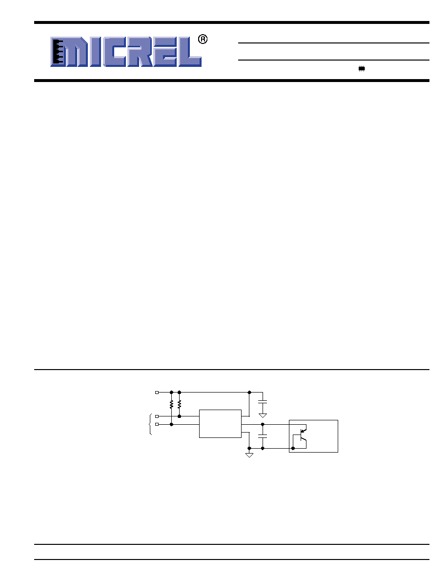
Typical Application
DATA
5
4
2
3
1
TO
SERIAL BUS
HOST
CPU DIODE
2000pF
MIC281
CLK
NC
3.3V
10k
pull-ups
VDD
T1
GND
0.1µF
MIC281 Typical Application
Features
∑ Remote temperature measurement using embedded
thermal diodes or commodity transistors
∑ Accurate remote sensing
±3∞C max., 0∞C to 100∞C
∑ Excellent noise rejection
∑ I
2
C and SMBus 2.0 compatible serial interface
∑ SMBus timeout to prevent bus lockup
∑ Voltage tolerant I/Os
∑ Low power shutdown mode
∑ Failsafe response to diode faults
∑ 3.0V to 3.6V power supply range
∑ IttyBittyTM SOT23-6 Package
Applications
∑ Desktop, server and notebook computers
∑ Set-top boxes
∑ Game consoles
∑ Appliances
Micrel, Inc. ∑ 2180 Fortune Drive ∑ San Jose, CA 95131 ∑ USA ∑ tel + 1 (408) 944-0800 ∑ fax + 1 (408) 474-1000 ∑ http://www.micrel.com
IttyBitty is a registered trademark of Micrel, Inc.
*All trademarks are the property of their respective owners.
MIC281
Micrel
MIC281
2
November 2004
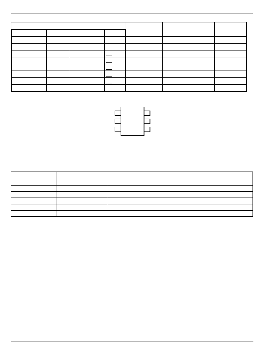
Pin Configuration
1
VDD
GND
T1
6
5
NC
DATA
CLK
4
2
3
SOT23-6
Pin Description
Pin
Pin Name
Pin Description
1
VDD
Analog Input: Power supply input to the IC.
2
GND
Ground return for all IC functions.
3
T1
Analog Input: Connection to remote diode junction.
4
CLK
Digital Input: Serial bit clock input.
5
DATA
Digital I/O: Open-drain. Serial data input/output.
6
NC
No Connection: Must be left unconnected.
Ordering Information
Part Number
Slave Address Ambient Temp. Range
Package
Standard
Marking Pb-FREE
Marking
MIC281-0BM6* TB00
MIC281-0YM6* TB00
1001 000x
b
-55∞C to +125∞C
SOT23-6
MIC281-1BM6* TB01
MIC281-1YM6* TB01
1001 001x
b
-55∞C to +125∞C
SOT23-6
MIC281-2BM6* TB02
MIC281-2YM6* TB02
1001 010x
b
-55∞C to +125∞C
SOT23-6
MIC281-3BM6* TB03
MIC281-3YM6* TB03
1001 011x
b
-55∞C to +125∞C
SOT23-6
MIC281-4BM6 TB04
MIC281-4YM6
TB05
1001 100x
b
-55∞C to +125∞C
SOT23-6
MIC281-5BM6* TB05
MIC281-5YM6* TB05
1001 101x
b
-55∞C to +125∞C
SOT23-6
MIC281-6BM6* TB06
MIC281-6YM6* TB06
1001 110x
b
-55∞C to +125∞C
SOT23-6
MIC281-7BM6* TB07
MIC281-7YM6* TB07
1001 111x
b
-55∞C to +125∞C
SOT23-6
* Contact Micrel regarding availability

November 2004
3
MIC281
MIC281
Micrel
Absolute Maximum Ratings
(Note 1)
Power Supply Voltage, V
DD .....................................................
3.8V
Voltage on T1 ........................................≠0.3V to V
DD
+0.3V
Voltage on CLK, DATA ....................................≠0.3V to 6.0V
Current Into Any Pin ................................................. ±10mA
Power Dissipation, T
A
= 125∞C ................................ 109mW
Junction Temperature ................................................ 150∞C
Storage Temperature ................................ ≠65∞C to +150∞C
ESD Ratings,
Note 7
Human Body Model ................................................ 1.5kV
Machine Model ........................................................ 200V
Soldering (SOT23-6 Package)
Vapor Phase (60s) .........................................220
+5
/
≠0
∞C
Infrared (15s) .................................................235
+5
/
≠0
∞C
Operating Ratings
(Note 2)
Power Supply Voltage, V
DD
......................... +3.0V to +3.6V
Ambient Temperature Range (T
A
) .............. ≠40∞C to +85∞C
Package Thermal Resistance (
JA
)
SOT-23-6 ...........................................................230∞C/W
Electrical Characteristics
For typical values, T
A
=25∞C, V
DD
=3.3V unless otherwise noted.
Bold values are for T
MIN
T
A
T
MAX
unless otherwise noted.
Note 2
Symbol
Parameter
Condition
Min
Typ
Max
Units
Power Supply
I
DD
Supply Current
T1 open; CLK=DATA=High; Normal Mode
0.23
0.4
mA
Shutdown mode; T1 open; CLK = 100kHz;
9
µA
Note 5
Shutdown Mode; T1 open; CLK=DATA=High
6
µA
t
POR
Power-on reset time,
Note 5
V
DD
> V
POR
200
µs
V
POR
Power-on reset voltage
All registers reset to default values; A/D
2.65
2.95
V
conversions initiated
V
HYST
Power-on reset hysteresis voltage
300
mV
Note 5
Temperature-to-Digital Converter Characteristics
Accuracy,
Notes 3, 5, 6
0∞C T
D
100∞C; 0∞C T
A
85∞C;
±
1
±
3
∞C
3.15V V
DD
3.45V
≠40∞C T
D
125∞C; 0∞C T
A
85∞C;
±
2
±
5
∞C
3.15V V
DD
3.45V
t
CONV
Conversion time,
Note 5
200
240
ms
Remote Temperature Input, T1
I
F
Current into External Diode
T1 forced to 1.0V, high level
192
400
µA
Note 5
Low level
7
12
µA
Serial Data I/O Pin, DATA
V
OL
Low Output Voltage,
Note 4
I
OL
= 3mA
0.3
V
I
OL
= 6mA
0.5
V
V
IL
Low Input Voltage
3.0V V
DD
5.5V
0.8
V
V
IH
High Input Voltage
3.0V V
DD
5.5V
2.1
5.5
V
C
IN
Input Capacitance,
Note 5
10
pF
I
LEAK
Input Current
±
1
µA

MIC281
Micrel
MIC281
4
November 2004
Symbol
Parameter
Condition
Min
Typ
Max
Units
Serial Clock Input, CLK
V
IL
Low Input Voltage
3.0V V
DD
3.6V
0.8
V
V
IH
High Input Voltage
3.0V V
DD
3.6V
2.1
5.5
V
C
IN
Input Capacitance,
Note 5
10
pF
I
LEAK
Input current
±1
µA
Serial Interface Timing
t
1
CLK (clock) period
2.5
µs
t
2
Data in Setup Time to CLK High
100
ns
t
3
Data Out Stable After CLK Low
300
ns
t
4
DATA Low Setup Time to CLK Low
Start Condition
100
ns
t
5
DATA High Hold Time After CLK High Stop Condition
100
ns
t
TO
Bus timeout
25
30
35
ms
Note 1. The device is not guaranteed to function outside its operating range.
Note 2. Final test on outgoing product is performed at T
A
= 25∞C.
Note 3. T
D
is the temperature of the remote diode junction. Testing is performed using a single unit of one of the transistors listed in Table 5.
Note 4. Current into the DATA pin will result in self-heating of the device. Sink current should be minimized for best accuracy.
Note 5. Guaranteed by design over the operating temperature range. Not 100% production tested.
Note 6. Accuracy specifications do not include quantization noise which may be up to ± 0.5LSB.
Note 7. Devices are ESD sensitive. Observe appropriate handling precautions.
Timing Diagram
t
1
t
2
t
5
t
4
t
3
SCL
SDA
DATA INPUT
SDA
DATA OUTPUT
Serial Interface Timing

November 2004
5
MIC281
MIC281
Micrel
Typical Characteristics
V
DD
= 3.3V; T
A
= 25∞C, unless otherwise noted.
-20
-15
-10
-5
0
5
0
1000
2000
3000
4000
5000
6000
7000
8000
TEMPERATURE ERROR
(
∞
C)
CAPACITANCE (pF)
R emote T emperature E rror vs .
C apacitanc e on T 1
0
0.2
0.4
0.6
0.8
1.0
1.2
1.4
1.6
TEMPERTURE ERROR
(
∞
C)
E rror Due to Nois e on the
C ollec tor of R emote T rans is tor
FREQUENCY (Hz)
1 10 100 1k 10k 100k 1M 10M100M
50mV
P -P
25mV
P -P
100mV
P -P
0
50
100
150
200
250
300
350
400
-55 -35 -15 5 25 45 65 85 105 125
SUPPLY CURRENT
(
µ
A)
TEMPERATURE (∞C)
S upply C urrent vs .
T emperature for V
DD
= 3.3V
0
5
10
15
20
0
100
200
300
400
QUIESCENT CURRENT
(
µ
A)
FREQUENCY (kHz)
Quies c ent C urrent vs .
C loc k F requency in
S hutdown Mode
T 1 open
DAT A = HIG H
0
1
2
3
4
5
6
7
8
9
10
2.6
2.8
3.0
3.2
3.4
3.6
QUIESCENT CURRENT
(
µ
A)
SUPPLY VOLTAGE (V)
Quies c ent C urrent vs .
S upply V oltage in S hutdown Mode
T 1 open
C LK = DAT A = HIG H
-8
-6
-4
-2
0
2
4
6
8
1x10
6
1x10
7
1x10
8
1x10
9
MEASUREMENT ERROR
(
∞
C)
RESISTANCE FROM T1 ()
Meas urement E rror vs .
P C B L eakage to +3.3V /G ND
G ND
3.3V
0
5
10
15
20
25
30
-55 -35 -15 5 25 45 65 85 105 125
QUIESCENT CURRENT
(
µ
A)
TEMPERATURE (∞C)
Quies c ent C urrent vs .
T emperature in S hutdown Mode
T 1 open
C LK = DAT A = HIG H
0
1
2
3
4
5
6
7
REMOTE TEMP. ERROR
(
∞
C)
E rror Due to Nois e on the B as e
of R emote T rans is tor
FREQUENCY (Hz)
1 10 100 1k 10k 100k 1M 10M100M
3mV
P -P
25mV
P -P
10mV
P -P
-2
-1.5
-1
-0.5
0
0.5
1
1.5
2
0
20
40
60
80
100
MEASUREMENT ERROR
(
∞
C)
REMOTE DIODE TEMPERATURE (∞C)
R emote T emperature
Meas urement E rror

MIC281
Micrel
MIC281
6
November 2004
Functional Description
Serial Port Operation
The MIC281 uses standard SMBus Write_Byte and Read_Byte
operations for communication with its host. The SMBus
Write_Byte operation involves sending the device's slave
address (with the R/W bit low to signal a write operation),
followed by a command byte and the data byte. The SMBus
Read_Byte operation is a composite write and read operation:
the host first sends the device's slave address followed by
the command byte, as in a write operation. A new start bit
must then be sent to the MIC281, followed by a repeat of the
slave address with the R/W bit (LSB) set to the high (read)
state. The data to be read from the part may then be clocked
out. These protocols are shown in Figures 1 and 2.
The Command byte is eight bits (one byte) wide. This byte
carries the address of the MIC281 register to be operated
upon. The command byte values corresponding to the various
MIC281 registers are shown in Table 1. Other command byte
values are reserved, and should not be used.
S 1 0 0 1 A2 A1 A0 0 A X X X X X X X X A
D4
D5
D6
D3 D2 D1 D0
D7
/A P
MIC281 Slave Address
DATA
CLK
Command Byte
Data Byte to MIC281
START
STOP
R/W = WRITE
ACKNOWLEDGE
ACKNOWLEDGE
NOT ACKNOWLEDGE
Master to slave transfer,
i.e., DATA driven by master.
Slave to master transfer,
i.e., DATA driven by slave.
Figure 1. Write_Byte Protocol
S 1 0 0 1 X X X
X X X
0 A X X X X X X X X A S 1
1
1
0 0
X
X
X
X X X X
A X
/A P
MIC281 Slave Address
DATA
CLK
Command Byte
MIC281 Slave Address
Data Read From MIC281
START
START
STOP
R/W = WRITE
R/W = READ
ACKNOWLEDGE
ACKNOWLEDGE
ACKNOWLEDGE
NOT ACKNOWLEDGE
Master to slave transfer,
i.e., DATA driven by master.
Slave to master transfer,
i.e., DATA driven by slave.
Figure 2. Read_Byte Protocol
Command Byte
Power-on
Target Register
Value
Default
Label
Description
Read
Write
TEMP
Remote temperature result
01
h
n/a
00
h
(0∞C)
CONFIG
Configuration
03
h
03
h
80
h
MFG_ID
Manufacturer identification
FE
h
n/a
2A
h
DEV_ID
Device and revision identification
FF
h
n/a
0x
h
*
* The lower nibble contains the die revision level, e.g., Rev 0 = 00h.
Table 1. MIC281 Register Addresses

November 2004
7
MIC281
MIC281
Micrel
Slave Address
The MIC281 will only respond to its own unique slave ad-
dress. A match between the MIC281's address and the
address specified in the serial bit stream must be made to
initiate communication. The MIC281's slave address is fixed
at the time of manufacture. Eight different slave addresses
are available as determined by the part number. See Table
2 below and the Ordering Information table.
Part Number
Slave Address
MIC281-0BM6
1001 000x
b
= 90
h
MIC281-1BM6
1001 001x
b
= 92
h
MIC281-2BM6
1001 010x
b
= 94
h
MIC281-3BM6
1001 011x
b
= 96
h
MIC281-4BM6
1001 100x
b
= 98
h
MIC281-5BM6
1001 101x
b
= 9A
h
MIC281-6BM6
1001 110x
b
= 9C
h
MIC281-7BM6
1001 111x
b
= 9E
h
Table 2. MIC281 Slave Addresses
Temperature Data Format
The least-significant bit of the temperature register represents
one degree Centigrade. The values are in a two's comple-
ment format, wherein the most significant bit (D7) represents
the sign: zero for positive temperatures and one for negative
temperatures. Table 3 shows examples of the data format
used by the MIC281 for temperatures.
Temperature
Binary
Hex
+127∞C
0111 1111
7F
+125∞C
0111 1101
7D
+25∞C
0001 1001
19
+1∞C
0000 0001
01
0∞C
0000 0000
00
≠1∞C
1111 1111
FF
≠25∞C
1110 0111
E7
≠125∞C
1000 0011
83
≠128∞C
1000 0000
80
Table 3. Digital Temperature Format
Diode Faults
The MIC281 is designed to respond in a failsafe manner to
diode faults. If an internal or external fault occurs in the tem-
perature sensing circuitry, such as T1 being open or shorted
to V
DD
or GND, the temperature result will be reported as the
maximum full-scale value, +127∞C. Note that diode faults will
not be detected until the first A/D conversion cycle is completed
following power-up or exiting shutdown mode.
Shutdown Mode
Setting the shutdown bit in the configuration register will
cause the MIC281 to cease operation. The A/D converter will
stop and power consumption will drop to the I
SHDN
level. No
registers will be affected by entering shutdown mode. The
last temperature reading will persist in the TEMP register.

MIC281
Micrel
MIC281
8
November 2004
Remote Temperature Result (TEMP)
8-bits, read-only
Remote Temperature Result Register
D[7]
D[6]
D[5]
D[4]
D[3]
D[2]
D[1]
D[0]
read-only
read-only
read-only
read-only
read-only
read-only
read-only
read-only
Temperature Data from ADC
Bit
Function
Operation
D[7:0]
Measured temperature data for the remote zone
Read-only
Power-up default value: 0000 0000
b
= 00
h
(0∞C)**
Command byte:
0000 0001
b
= 01
h
Each LSB represents one degree centigrade. The values are in a two's complement binary format such that 0∞C is reported
as 0000 0000b. See Temperature Data Format (above) for more details.
**TEMP will contain measured temperature data after the completion of one conversion.
Configuration Register (CONFIG)
8-bits, read/write
Configuration Register
D[7]
D[6]
D[5]
D[4]
D[3]
D[2]
D[1]
D[0]
reserved
reserved
reserved
reserved
reserved
reserved
reserved
write-only
Reserved
Shutdown
reserved
(SHDN)
Bits(s)
Function
Operation*
D7
Reserved
Always write as zero;
reads undefined
SHDN
Shutdown bit
0 = normal operation, 1 =
shutdown
D[5:0]
Reserved
Always write as zero;
reads undefined
Power-up default value: x0xx xxxx
b
(Not in shutdown mode)
Command byte:
0000 0011
b
= 03
h
* Any write to CONFIG will result in any A/D conversion in progress being aborted and the result discarded. The A/D will begin a new conver-
sion sequence once the write operation is complete.
Detailed Register Descriptions

November 2004
9
MIC281
MIC281
Micrel
Manufacturer ID Register (MFG_ID)
8-bits, read-only
Manufacturer ID Register
D[7]
D[6]
D[5]
D[4]
D[3]
D[2]
D[1]
D[0]
read-only
read-only
read-only
read-only
read-only
read-only
read-only
read-only
0
0
1
0
1
0
1
0
BIT(S)
FUNCTION
Operation*
D[7:0]
Identifies Micrel as the manufacturer of the device. Always returns 2A
h
.
Read-only. Always returns 2A
h
.
Power-up default value:
0010 1010
b
= 2A
h
Read command byte:
1111 1110
b
= FE
h
Die Revision Register (DIE_REV)
8-bits, read-only
Die Revision Register
D[7]
D[6]
D[5]
D[4]
D[3]
D[2]
D[1]
D[0]
read-only
read-only
read-only
read-only
read-only
read-only
read-only
read-only
MIC281 DIE REVISION NUMBER
Bit(s)
Function
Operation*
D[7:0]
Identifies the device revision number
Read-only
Power-up default value:
[Device revision number]
h
Read command byte:
1111 1111
b
= FF
h

MIC281
Micrel
MIC281
10
November 2004
Application Information
Remote Diode Selection
Most small-signal PNP transistors with characteristics similar
to the JEDEC 2N3906 will perform well as remote temperature
sensors. Table 4 lists several examples of such parts that
Micrel has tested for use with the MIC281. Other transistors
equivalent to these should also work well.
Vendor
Part Number
Package
Fairchild Semiconductor
MMBT3906
SOT-23
On Semiconductor
MMBT3906L
SOT-23
Infineon Technologies
SMBT3906
SOT-23
Samsung Semiconductor
KST3906-TF
SOT-23
Table 4. Transistors Suitable for Use as Remote
Diodes
Minimizing Errors
Self-Heating
One concern when using a part with the temperature accuracy
and resolution of the MIC281 is to avoid errors induced by
self-heating (V
DD
◊ I
DD
) + (V
OL
◊ I
OL
). In order to understand
what level of error this might represent, and how to reduce
that error, the dissipation in the MIC281 must be calculated
and its effects reduced to a temperature offset. The worst-
case operating condition for the MIC281 is when V
DD
=
3.6V. The maximum power dissipated in the part is given in
Equation 1 below.
In most applications, the DATA pin will have a duty cycle of
substantially below 25% in the low state. These considerations,
combined with more typical device and application parameters,
give a better system-level view of device self-heating. This
is illustrated by Equation 2. In any application, the best ap-
proach is to verify performance against calculation in the final
application environment. This is especially true when dealing
with systems for which some temperature data may be poorly
defined or unobtainable except by empirical means.
P
D
= [(I
DD
◊
V
DD
)+(I
OL(DATA)
◊
V
OL(DATA)
)]
P
D
= [(0.4mA ◊ 3.6V)+(6mA ◊ 0.5V)]
P
D
= 4.44mW
R
(J-A)
of SOT23-6 package is 230∞C/W, therefore...
the theoretical maximum self-heating is:
4.44mW ◊ 230∞C/W = 1.02∞C
Equation 1. Worst-Case Self-Heating
P
D
= [(I
DD
◊
V
DD
)+(I
OL(DATA)
◊
V
OL(DATA)
)]
P
D
= [(0.23mA ◊ 3.3V)+(25% ◊ 1.5mA ◊ 0.15V)]
P
D
= 0.815mW
R
(J-A)
of SOT23-6 package is 230∞C/W, therefore...
the typical self-heating is:
0.815mW ◊ 230∞C/W = 0.188∞C
Equation 2. Real-World Self-Heating Example
Series Resistance
The operation of the MIC281 depends upon sensing the
V
CB-E
of a diode-connected PNP transistor ("diode ") at two dif-
ferent current levels. For remote temperature measurements,
this is done using an external diode connected between T1
and ground. Since this technique relies upon measuring the
relatively small voltage difference resulting from two levels of
current through the external diode, any resistance in series
with the external diode will cause an error in the temperature
reading from the MIC281. A good rule of thumb is this: for
each ohm in series with the external transistor, there will be a
0.9∞C error in the MIC281's temperature measurement. It is
not difficult to keep the series resistance well below an ohm
(typically < 0.1), so this will rarely be an issue.
Filter Capacitor Selection
It is usually desirable to employ a filter capacitor between the
T1 and GND pins of the MIC281. The use of this capacitor is
recommended in environments with a lot of high frequency
noise (such as digital switching noise), or if long traces or wires
are used to connect to the remote diode. The recommended
total capacitance from the T1 pin to GND is 2200pF. If the
remote diode is to be at a distance of more than 6"-12" from
the MIC281, using twisted pair wiring or shielded microphone
cable for the connections to the diode can significantly reduce
noise pickup. If using a long run of shielded cable, remember
to subtract the cable's conductor-to-shield capacitance from
the 2200pF total capacitance.

November 2004
11
MIC281
MIC281
Micrel
Layout Considerations
The following guidelines should be kept in mind when design-
ing and laying out circuits using the MIC281:
1. Place the MIC281 as close to the remote diode
as possible, while taking care to avoid severe
noise sources such as high frequency power
transformers, CRTs, memory and data busses,
etc.
2. Since any conductance from the various volt-
ages on the PC board and the T1 line can in-
duce serious errors, it is good practice to guard
the remote diode's emitter trace with a pair of
ground traces. These ground traces should be
returned to the MIC281's own ground pin. They
should not be grounded at any other part of their
run. However, it is highly desirable to use these
guard traces to carry the diode's own ground
return back to the ground pin of the MIC281,
thereby providing a Kelvin connection for the
base of the diode. See Figure 3.
3. When using the MIC281 to sense the tempera-
ture of a processor or other device which has an
integral thermal diode, e.g., Intel's Pentium III,
connect the emitter and base of the remote sen-
sor to the MIC281 using the guard traces and
Kelvin return shown in Figure 3. The collector of
the remote diode is typically inaccessible to the
user on these devices.
REMOTE DIODE (T1)
GUARD/RETURN
1
2
VDD
GND
T1
6
5
4
3
NC
DATA
CLK
GUARD/RETURN
MIC281
Figure 3. Guard Traces/Kelvin Ground Returns
4. Due to the small currents involved in the mea-
surement of the remote diode's V
BE
, it is
important to adequately clean the PC board after
soldering to prevent current leakage. This is
most likely to show up as an issue in situations
where water-soluble soldering fluxes are used.
5. In general, wider traces for the ground and T1
lines will help reduce susceptibility to radiated
noise (wider traces are less inductive). Use trace
widths and spacing of 10mm wherever possible
and provide a ground plane under the MIC281
and under the connections from the MIC281 to
the remote diode. This will help guard against
stray noise pickup.
6. Always place a good quality power supply
bypass capacitor directly adjacent to, or un-
derneath, the MIC281. This should be a 0.1µF
ceramic capacitor. Surface mount parts provide
the best bypassing because of their low
inductance.

MIC281
Micrel
MIC281
12
November 2004
Package Information
0.20 (0.008)
0.09 (0.004)
0.60 (0.024)
0.10 (0.004)
3.00 (0.118)
2.80 (0.110)
10∞
0∞
3.00 (0.118)
2.60 (0.102)
1.75 (0.069)
1.50 (0.059)
0.95 (0.037) REF
1.30 (0.051)
0.90 (0.035)
0.15 (0.006)
0.00 (0.000)
DIMENSIONS:
MM (INCH)
0.50 (0.020)
0.35 (0.014)
1.90 (0.075) REF
6-Lead SOT23 (M6)
MICREL INC. 2180 FORTUNE DRIVE SAN JOSE, CA 95131 USA
TEL
+ 1 (408) 944-0800
FAX
+ 1 (408) 474-1000
WEB
http://www.micrel.com
This information furnished by Micrel in this data sheet is believed to be accurate and reliable. However no responsibility is assumed by Micrel for its use.
Micrel reserves the right to change circuitry and specifications at any time without notification to the customer.
Micrel Products are not designed or authorized for use as components in life support appliances, devices or systems where malfunction of a product can
reasonably be expected to result in personal injury. Life support devices or systems are devices or systems that (a) are intended for surgical implant into
the body or (b) support or sustain life, and whose failure to perform can be reasonably expected to result in a significant injury to the user. A Purchaser's
use or sale of Micrel Products for use in life support appliances, devices or systems is a Purchaser's own risk and Purchaser agrees to fully indemnify
Micrel for any damages resulting from such use or sale.
© 2004 Micrel Incorporated