 | ÐлекÑÑоннÑй компоненÑ: MIC29512B | СкаÑаÑÑ:  PDF PDF  ZIP ZIP |
3-11 MIC29510 DB97
MIC29510/29512
Micrel
3-96
1997
Ordering Information
Part Number
Temp. Range*
Voltage
Current
Package
MIC29510-3.3BT
0
°
C to +125
°
C
3.3V
5.0A
TO-220-3
MIC29510-5.0BT
0
°
C to +125
°
C
5.0V
5.0A
TO-220-3
MIC29512BT
0
°
C to +125
°
C
Adj.
5.0A
TO-220-5
* Junction Temperature
General Description
The MIC29510 and MIC29512 are high-current, high-accu-
racy, low-dropout voltage regulators featuring fast transient
recovery from input voltage surges and output load current
changes. These regulators use a PNP pass element that
features Micrel's proprietary Super ßeta PNPTM process.
The MIC29510/2 is available in two versions: the three pin
fixed output MIC29510 and the five pin adjustable output
voltage MIC29512. All versions are fully protected against
overcurrent faults, reversed input polarity, reversed lead
insertion, overtemperature operation, and positive and nega-
tive transient voltage spikes.
A TTL compatible enable (EN) control pin supports external
on/off control. If on/off control is not required, the device may
be continuously enabled by connecting EN to IN.
The MIC29510/2 is available in the standard three and five
pin TO-220 package with an operating junction temperature
range of 0
°
C to +125
°
C.
For applications requiring even lower dropout voltage, input
voltage greater than 16V, or an error flag, see the MIC29500/
29501/29502/29503.
Features
· Fast transient response
· 5A current capability
· 700mV dropout voltage at full load
· Low ground current
· Accurate 1% guaranteed tolerance
· "Zero" current shutdown mode (MIC29512)
· Fixed voltage and adjustable versions
Applications
· PentiumTM and Power PCTM processor supplies
· High-efficiency "green" computer systems
· High-efficiency linear power supplies
· High-efficiency switching supply post regulator
· Battery-powered equipment
MIC29510/29512
5A Fast-Response LDO Regulator
Preliminary Information
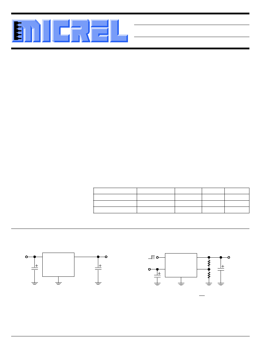
Typical Application
MIC29512
OUT
ADJ
R1
V
OUT
R2
EN
GND
V
IN
IN
On
Off
V
OUT
= 1. 240
R1
R2
+ 1
Fixed Regulator Configuration
MIC29510
OUT
V
OUT
IN
GND
V
IN
Adjustable Regulator Configuration
1997
3-97
MIC29510/29512
Micrel
3
Pin Description
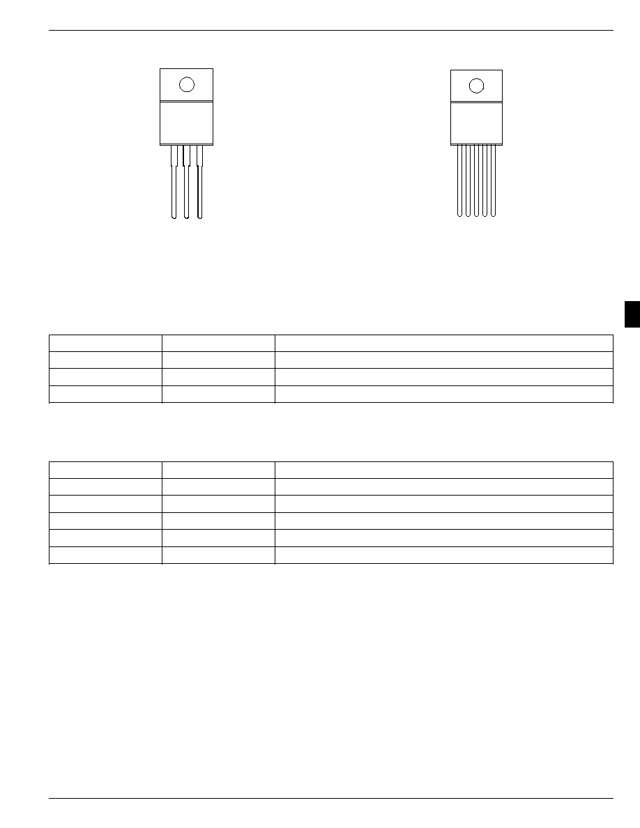
3-Pin TO-220 (MIC29510)
Pin Number
Pin Name
Pin Function
1
IN
Unregulated Input: +16V maximum supply.
2
GND
Ground: Internally connected to tab (ground).
3
OUT
Regulated Output
5-Pin TO-220 (MIC29512)
Pin Number
Pin Name
Pin Function
1
EN
Enable (Input): Logic-level ON/OFF control.
2
IN
Unregulated Input: +16V maximum supply.
3
GND
Ground: Internally connected to tab (ground).
4
OUT
Regulated Output
5
ADJ
Output Voltage Adjust: 1.240V feedback from external resistive divider.
Operating Ratings
Operating Junction Temperature ................. 0
°
C to +125
°
C
JC
(TO-220) ............................................................. 2
°
C/W
JA
(TO-220) ........................................................... 55
°
C/W
Absolute Maximum Ratings
Input Supply Voltage (Note 1) ....................... 20V to +20V
Power Dissipation .................................... Internally Limited
Storage Temperature Range ................... 65
°
C to +150
°
C
Lead Temperature (Soldering, 5 sec.) ...................... 260
°
C
Pin Configuration
1 2 3 4 5
MIC29512BT
1 2 3
MIC29510BT
On all devices, the Tab is grounded.

MIC29510/29512
Micrel
3-98
1997
Electrical Characteristics
All measurements at T
J
= 25
°
C unless otherwise noted. Bold values are guaranteed across the operating temperature range.
Parameter
Condition
Min
Typ
Max
Units
Output Voltage
10mA
I
O
I
FL
, (V
OUT
+ 1V)
V
IN
8V (Note 2)
2
2
%
Line Regulation
I
O
= 10mA, (V
OUT
+ 1V)
V
IN
8V
0.06
0.5
%
Load Regulation
V
IN
= V
OUT
+ 1V, 10mA
I
OUT
I
FULL LOAD
(Notes 2, 6)
0.2
1
%
V
O
/
T
Output Voltage Temperature Coefficient (Note 6)
20
100
ppm/
°
C
Dropout Voltage
V
OUT
= 1%, (Note 3)
MIC29510/29512 I
O
= 100mA
80
200
mV
I
O
= 750mA
200
mV
I
O
= 1.5A
320
mV
I
O
= 3A
500
mV
I
O
= 5A
700
1000
mV
Ground Current
MIC29510/29512 I
O
= 750mA, V
IN
= V
OUT
+ 1V
3
20
mA
I
O
= 1.5A
10
mA
I
O
= 3A
36
mA
I
O
= 5A
100
150
mA
I
GNDDO
Ground Pin
V
IN
= 0.5V less than specified V
OUT
. I
OUT
= 10mA
2
3
mA
Current at Dropout
Current Limit
MIC29510/29512 V
OUT
= 0V (Note 4)
5.0
6.5
A
e
n
, Output Noise Voltage
C
L
= 47
µ
F
260
µ
V
RMS
(10Hz to 100kHz) I
L
= 100mA
Reference (MIC29512 only)
Reference Voltage
10mA
I
O
I
FL
, V
OUT
+ 1V
V
IN
8V (Note 2)
1.215
1.265
V
MAX
Adjust Pin Bias Current
40
80
nA
120
nA
Reference Voltage
(Note 7)
20
ppm/
°
C
Temperature Coefficient
Adjust Pin Bias Current
0.1
nA/
°
C
Temperature Coefficient
1997
3-99
MIC29510/29512
Micrel
3
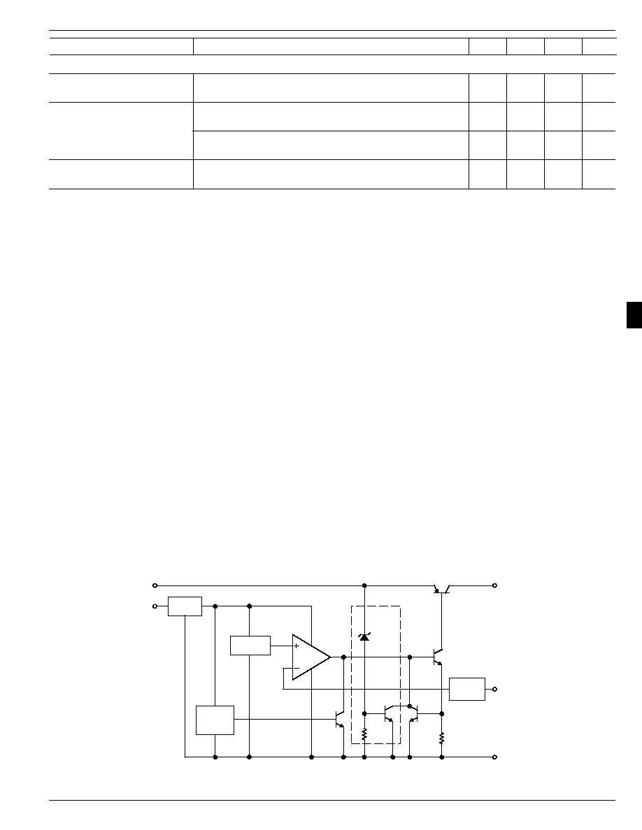
On/Off
Reference
Bias
Feed-
back
GND
28V
OUT
ADJ
EN
IN
O.V.
I
LIMIT
Thermal
Shut-
down
Block Diagram
Enable Input (MIC29512 only)
Input Logic Voltage
Low (Off)
0.8
V
High (On)
2.4
V
Enable (EN) Pin Input Current
V
EN
= V
IN
15
30
µ
A
75
µ
A
V
EN
= 0.8V
2
µ
A
4
µ
A
Regulator Output
(Note 8)
10
µ
A
Current in Shutdown
20
µ
A
General Note: Devices are ESD sensitive. Handling precautions recommended.
Note 1:
The maximum continuous supply voltage is 16V.
Note 2:
Full Load current is defined as 5A for the MIC29510/29512. For testing, V
OUT
is programmed to 5V.
Note 3:
Dropout voltage is defined as the input-to-output differential when the output voltage drops to 99% of its nominal value with V
OUT
+ 1V applied
to V
IN
.
Note 4:
For this test, V
IN
is the larger of 8V or V
OUT
+ 3V.
Note 5:
Ground pin current is the regulator quiescent current. The total current drawn from the source is the sum of the load current plus the ground
pin current.
Note 6:
Output voltage temperature coefficient is defined as the worst case voltage change divided by the total temperature range.
Note 7:
V
REF
V
OUT
(V
IN
1 V), 2.4V
V
IN
16V, 10mA < I
L
I
FL
, T
J
T
J MAX.
Note 8:
V
EN
0.8V and V
IN
8V, V
OUT
= 0.
Parameter
Conditions
Min
Typical
Max
Units
16V
MIC29510/29512
Micrel
3-100
1997
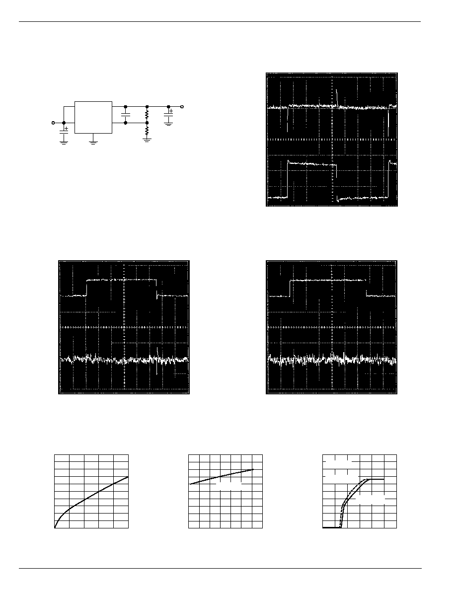
Typical Characteristics
V
IN
= V
OUT
+ 1V
MIC29512
EN
IN
OUT
ADJ
GND
0.1µF
93.1k
1%
49.9k
1%
V
OUT
3.525V nominal
4
×
330µF
AVX
TPSE337M006R0100
tantalum
V
OUT
load (not shown):
Intel® Power Validator
MIC29512 Load Transient Response Test Circuit
0mA
200mA
5A
3.525V
+20mV
20mV
LOAD CURRENT OUTPUT VOLTAGE
MIC29512 Load Transient Response
(See Test Circuit Schematic)
1ms/division
0
0.2
0.4
0.6
0.8
1.0
0
1
2
3
4
5
DROPOUT VOLTAGE (V)
OUTPUT CURRENT (A)
MIC2951x Dropout Voltage
vs. Output Current
0
0.2
0.4
0.6
0.8
1.0
-60 -30
0
30
60
90 120 150
DROPOUT VOLTAGE (V)
TEMPERATURE (
°
C)
MIC2951x Dropout Voltage
vs. Temperature
I
LOAD
= 5A
0.0
1.0
2.0
3.0
4.0
5.0
0
2
4
6
OUTPUT VOLTAGE (V)
INPUT VOLTAGE (V)
MIC29510-3.3
Dropout Characteristics
I
LOAD
= 5A
I
LOAD
= 10mA
V
IN
= 4.3V
6.525V
4.525V
3.525V
+20mV
20mV
OUTPUT VOLTAGE INPUT VOLTAGE
MIC29512 Line Transient Response
with 5A Load, 10
µ
F Output Capacitance
200
µ
s/division
I
OUT
= 5A
C
OUT
= 10
µ
F
6.525V
4.525V
3.525V
+20mV
20mV
OUTPUT VOLTAGE INPUT VOLTAGE
MIC29512 Line Transient Response
with 5A Load, 100
µ
F Output Capacitance
200
µ
s/division
I
OUT
= 5A
C
OUT
= 100
µ
F